STM805T中文资料
NCV8450STT3G;中文规格书,Datasheet资料
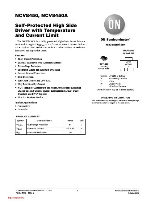
NCV8450, NCV8450ASelf-Protected High Side Driver with Temperatureand Current LimitThe NCV8450/A is a fully protected High−Side Smart Discrete device with a typical R DS(on) of 1.0 W and an internal current limit of 0.8 A typical. The device can switch a wide variety of resistive, inductive, and capacitive loads.Features•Short Circuit Protection•Thermal Shutdown with Automatic Restart •Overvoltage Protection•Integrated Clamp for Inductive Switching•Loss of Ground Protection•ESD Protection•Slew Rate Control for Low EMI•Very Low Standby Current•NCV Prefix for Automotive and Other Applications Requiring Unique Site and Control Change Requirements; AEC−Q100 Qualified and PPAP Capable•This is a Pb−Free DeviceTypical Applications•Automotive•IndustrialPRODUCT SUMMARYSymbolCharacteristics Value Unit V IN_CL Overvoltage Protection54V V D(on)Operation Voltage 4.5 − 45V R on On−State Resistance 1.0WMARKINGDIAGRAM1AYWXXXXX GGXXXXX= V8450 or 8450AA= Assembly LocationY= YearW= Work WeekG= Pb−Free Package(Note: Microdot may be in either location)SOT−223(TO−261)CASE 318ESee detailed ordering and shipping information in the package dimensions section on page 8 of this data sheet.ORDERING INFORMATIONFigure 1. Block Diagram V (Pins 2, 4)OUT(Pin 3)IN(Pin 1)PACKAGE PIN DESCRIPTIONPin #Symbol Description1IN Control Input, Active Low2V D Supply Voltage3OUT Output4V D Supply VoltageMAXIMUM RATINGSRatingSymbol ValueUnit Min Max DC Supply Voltage (Note 1)V D −1645V Load Dump Protection(RI = 2 W , t d = 400 ms, V IN = 0, 10 V, I L = 150 mA, V bb = 13.5 V)V Loaddump100V Input CurrentIin −1515mAOutput Current (Note 1)I out Internally Limited A Total Power Dissipation@ T A = 25°C (Note 2)@ T A = 25°C (Note 3)P D1.131.60WElectrostatic Discharge (Note 4)(Human Body Model (HBM) 100 pF/1500 W )Input All other15kVSingle Pulse Inductive Load Switching Energy (Note 4)(V DD = 13.5 V, I = 465 mApk, L = 200 mH, T JStart = 150°C)E AS 29mJ Operating Junction Temperature T J −40+150°C Storage TemperatureT storage−55+150°CStresses exceeding Maximum Ratings may damage the device. Maximum Ratings are stress ratings only. Functional operation above the Recommended Operating Conditions is not implied. Extended exposure to stresses above the Recommended Operating Conditions may affect device reliability.1.Reverse Output current has to be limited by the load to stay within absolute maximum ratings and thermal performance.2.Minimum Pad.3. 1 in square pad size, FR −4, 1 oz Cu.4.Not subjected to production testing.THERMAL RESISTANCE RATINGSParameterSymbol Max Value Unit Thermal Resistance (Note 5)Junction −to −Ambient (Note 2)Junction −to −Ambient (Note 3)R q JA R q JA11078.3K/W5.Not subjected to production testing.Figure 2. Applications Test CircuitELECTRICAL CHARACTERISTICS (6 v V D v 45 V; −40°C <T J < 150°C unless otherwise specified)Rating Symbol ConditionsValueUnit Min Typ MaxOUTPUT CHARACTERISTICSOperating Supply Voltage V SUPPLY 4.5−45VOn Resistance(Pin 1 Connected to GND)R ON T J = 25°C , I OUT = 150 mA, V D = 7 V − 45 VT J = 150°C, I OUT = 150 mA, V D = 7 V − 45 V(Note 6)T J = 25°C , I OUT= 150 mA, V D = 6 V1.01.41.1232.1WStandby Current (Pin 1 Open)I D V D v 20 VV D> 20 V 0.610100m AINPUT CHARACTERISTICSInput Current – Off State I IN_OFF V OUT v 0.1 V, R L = 270 W, T J = 25°CV OUT v 0.1V, R L= 270 W, T J = 150°C (Note 6)−50−40m AInput Current – On State(Pin 1 Grounded)I IN_ON 1.53mA Input Resistance (Note 6)R IN1k W SWITCHING CHARACTERISTICSTurn−On Time (Note 7)(V IN = V D to 0 V) to 90% V OUT t ON R L = 270 W(Note 6)V D = 13.5 V, R L = 270 W, T J = 25°C30125100m sTurn−Off Time (Note 7)(V IN= 0 V to V D) to 10% V OUT t OFF R L = 270 W (Note 6)V D = 13.5 V, R L = 270 W, T J = 25°C60175150m sSlew Rate On (Note 7)(V IN = V D to 0V) 10% to 30% V OUT dV/dt ON R L = 270 W(Note 6)V D = 13.5 V, R L = 270 W, T J = 25°C0.744V/m sSlew Rate Off (Note 7)(V IN= 0 V to V D) 70% to 40% V OUT dV/dt OFF R L = 270 W (Note 6)V D = 13.5 V, R L = 270 W, T J = 25°C0.944V/m sOUTPUT DIODE CHARACTERISTICS (Note 6)Drain−Source Diode Voltage V F I OUT = −0.2 A0.6V Continuous Reverse DrainCurrentI S T J = 25°C0.2A PROTECTION FUNCTIONS (Note 8)Temperature Shutdown (Note 6)T SD150175−°C Temperature ShutdownHysteresis (Note 6)T SD_HYST5°COutput Current Limit I LIM T J = −40°C, V D = 13.5 V, t m = 100 m s (Note 6)T J = 25 °C, V D = 13.5 V, t m = 100 m sT J = 150 °C , V D = 13.5 V, t m = 100 m s (Note 6)0.50.81.5AOutput Clamp Voltage(Inductive Load Switch Off)At V OUT = V D− V CLAMPV CLAMP I OUT = 4 mA4552VOvervoltage Protection V IN_CL I CLAMP = 4 mA5054V6.Not subjected to production testing7.Only valid with high input slew rates8.Protection functions are not designed for continuous repetitive operation and are considered outside normal operating rangeR D S (o n ) (W )TEMPERATURE (°C)Figure 3. R DS(on) vs. TemperatureR D S (o n ) (W )OUTPUT LOAD (A)Figure 4. R DS(on) vs. Output LoadV D (V)Figure 5. R DS(on) vs. V DR D S (o n ) (W )1020304050607080T U R N O N T I M E (m s )TEMPERATURE (°C)Figure 6. Turn On Time vs. TemperatureTEMPERATURE (°C)Figure 7. Turn Off Time vs. TemperatureT U R N O F F T I M E (m s )S L E W R A T E (O N ) (V /m s )TEMPERATURE (°C)Figure 8. Slew Rate (ON) vs. Temperature−40−20020406080100120140−40−20020406080100120140−TEMPERATURE (°C)Figure 9. Slew Rate (OFF) vs. Temperature S L E W R A T E (O F F ) (V /m s )TEMPERATURE (°C)Figure 10. Current Limit vs. TemperatureC U R R E N T L I M I T (A )P E A K S C C U R R E N T (A )V D , VOLTAGE (V)Figure 11. Peak Short Circuit Current vs. V DVoltageTEMPERATURE (°C)Figure 12. V D Leakage Current vs.Temperature Off −StateV D , L E A K A G E C U R R E N T (m A )V D , L E A K A G E C U R R E N T (m A )V D , VOLTAGE (V)Figure 13. V D Leakage Current vs. V D VoltageOff −State TEMPERATURE (°C)Figure 14. On −State Input Current vs.TemperatureI N P U T C U R R E N T (m A )V D , VOLTAGE (V)Figure 15. Output Voltage vs. V D VoltageO U T P U T V O L T A G E (V )V D , VOLTAGE (V)Figure 16. Input Current vs. V D VoltageOn −StateI N P U T C U R R E N T (m A )LOAD INDUCTANCE (mH)Figure 17. Single Pulse Maximum Switch −offCurrent vs. Load InductanceC U R R E N T (m A )V D , VOLTAGE (V)Figure 18. Input Current vs. V D VoltageOff −StateI N P U T C U R R E N T (m A )−S H U T D O W N T I M E (m s )TEMPERATURE (°C)Figure 19. Initial Short −Circuit Shutdown Timevs. TemperaturePULSE TIME (s)R (t ), E F F E C T I V E T R A N S I E N T T H E R M AL R E S P O N S ECOPPER HEAT SPREADER AREA (mm 2)R q J A (°C /W )06080100120140Figure 20. R q JA vs. Copper Area2040Figure 21. Transient Thermal ResponseISO PULSE TEST RESULTSTest PulseTest Level Test ResultsPulse Cycle Time and Generator Impedance1200 V C 500 ms, 10 W 2150 V C 500 ms, 10 W 3a 200 V C 100 ms, 50 W 3b 200 V C 100 ms, 50 W 5175 VE(100 V)400 ms, 2 WORDERING INFORMATIONDevicePackage Shipping †NCV8450STT3G SOT −223(Pb −Free)4000 / Tape & Reel NCV8450ASTT3GSOT −223(Pb −Free)4000 / Tape & Reel†For information on tape and reel specifications, including part orientation and tape sizes, please refer to our Tape and Reel Packaging Specifications Brochure, BRD8011/D.PACKAGE DIMENSIONSSOT −223 (TO −261)CASE 318E −04ISSUE MNOTES:1.DIMENSIONING AND TOLERANCING PER ANSI Y14.5M, 1982.2.CONTROLLING DIMENSION: INCH.DIM A MIN NOM MAX MIN MILLIMETERS1.50 1.63 1.750.060INCHESA10.020.060.100.001b 0.600.750.890.024b1 2.90 3.06 3.200.115c 0.240.290.350.009D 6.30 6.50 6.700.249E 3.30 3.50 3.700.130e 2.20 2.30 2.400.0870.850.94 1.050.0330.0640.0680.0020.0040.0300.0350.1210.1260.0120.0140.2560.2630.1380.1450.0910.0940.0370.041NOM MAX L1 1.50 1.75 2.000.0606.707.007.300.2640.0690.0780.2760.287H E−−e10°10°0°10°q*For additional information on our Pb −Free strategy and solderingdetails, please download the ON Semiconductor Soldering and Mounting Techniques Reference Manual, SOLDERRM/D.SOLDERING FOOTPRINT*ON Semiconductor and are registered trademarks of Semiconductor Components Industries, LLC (SCILLC). SCILLC reserves the right to make changes without further notice to any products herein. SCILLC makes no warranty, representation or guarantee regarding the suitability of its products for any particular purpose, nor does SCILLC assume any liability arising out of the application or use of any product or circuit, and specifically disclaims any and all liability, including without limitation special, consequential or incidental damages.“Typical” parameters which may be provided in SCILLC data sheets and/or specifications can and do vary in different applications and actual performance may vary over time. All operating parameters, including “Typicals” must be validated for each customer application by customer’s technical experts. SCILLC does not convey any license under its patent rights nor the rights of others. SCILLC products are not designed, intended, or authorized for use as components in systems intended for surgical implant into the body, or other applications intended to support or sustain life, or for any other application in which the failure of the SCILLC product could create a situation where personal injury or death may occur. Should Buyer purchase or use SCILLC products for any such unintended or unauthorized application, Buyer shall indemnify and hold SCILLC and its officers, employees, subsidiaries, affiliates,and distributors harmless against all claims, costs, damages, and expenses, and reasonable attorney fees arising out of, directly or indirectly, any claim of personal injury or death associated with such unintended or unauthorized use, even if such claim alleges that SCILLC was negligent regarding the design or manufacture of the part. SCILLC is an Equal Opportunity/Affirmative Action Employer. This literature is subject to all applicable copyright laws and is not for resale in any manner.PUBLICATION ORDERING INFORMATION分销商库存信息: ONSEMINCV8450STT3G。
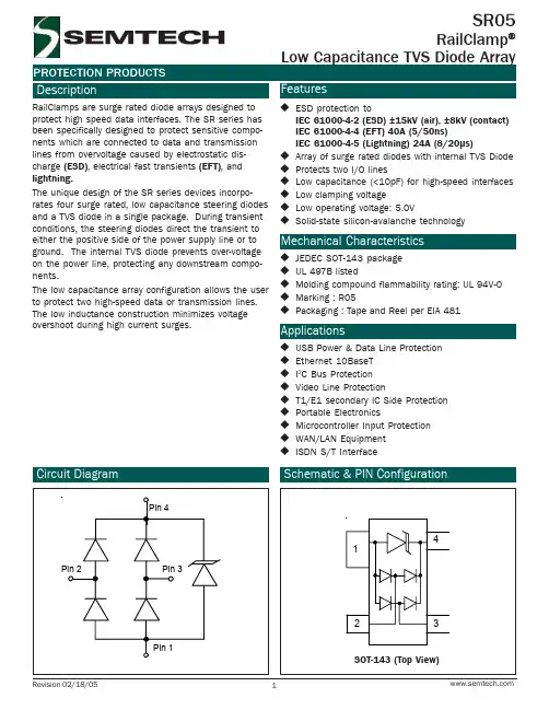
SR05.TCT中文资料
Forward Voltage vs. Forward Current
10 9
% Change in Capacitance 0 -2 -4 -6 -8 -10 -12 -14 -16
Capacitance vs. Reverse Voltage
Forward Voltage - V F (V)
8 7 6 5 4 3 2 1 0 0 5 10 15 20 25 30 35 40 45 50 Forward Current - IF (A) Waveform Parameters: tr = 8µs td = 20µs
SR05
Mechanical Characteristics
JEDEC SOT-143 package UL 497B listed Molding compound flammability rating: UL 94V-0 Marking : R05 Packaging : Tape and Reel per EIA 481
0
25
50
75
100
125
150
Ambient Temperature - TA (oC)
Pulse Waveform
110 100 90 80 Percent of IPP 70 60 50 40 30 20 10 0 0 5 10 15 Time (µs) 20 25 30 td = IPP/2 e
10 Peak Pulse Power - PPk (kW)
Power Derating Curve
1IP 90 80 70 60 50 40 30 20 10 0
1
0.1
Tektronix C805-C815 产品说明书
FACTORY CALIBRATION PROCEDURECONTENTS:GeneralC-805C ircuit specifications C-807Calibration procedure C-809Special test equipmentC-815INTRODUCTION:This isn 't a field recalibration procedure as is the procedure in your instruction manual. This is a guide in calibrating brand-new instrum ents, just Publication:assem bled instrum ents that have never been turned 061-105on before. Therefore it calls out many procedures February 1963and adjustments that a re rare ly required for subsequent recalibration.Even though we wrote this procedure prim arily for our own factory test departm ent, it's valuable to others also if used with some caution:!. Special test equipment, if mentioned, is not available from Tektronix unless it's listed also in our current catalog. This special equipment is used in our test department to speed calibration. Usually you can either duplicate its function with standard equipment in your facility, devise alternate approaches, or build the special test equipment yourself.For 53A, 53/54A and A units, all se ria l num bers.53A sn 101 to 149953/54A sn 1500 to 2797Asn 2798 upThe 53/54Aand A a re identical, only the nomenclature changed. Circuitry and circuit symbol numbers are different in the 53A but specifications are the sam e.2. Factory circuit specifications are not guaranteed unless they also appear as catalog or instruction manual specifications. Factory circuit specs usually are tighter than advertised specs. This helps insure the instrum ent will m eet or exceed advertised specs after shipment and during subsequent field recalibrations over several years of use. Your instrum ent may not meet factory circuit specs but should m eet catalog or instruction manual specs.3, Presetting internal adjustm ents, if mentioned, usually is unnecessary. This is helpful for "first-tim e" calibration only. If internal adjustments are p reset, you'll have to perform a 100% recalibration. So don't preset them unless you're certain a "start-fro m - scratch" policy is the best.In this procedure, all front panel controls for the instrum ent under test are in capital letters (SENSITIVITY) and internal adjustments are capitalized only (Gain Adj).A FCP A CALIBRATION2-9-63ABBREVIATIONS:a ampac alternating currentapprox approximatelyb basebulb light, lamp, etc.c collectorccw counterclockwise or full counterclockwise cer ceram iccm centim etercomp composition (resistor)cps cycles per seconde rt cathode ray tubecw clockwise or full clockwisedb decibeldc direct currentdiv divisione em itteremc electrolytic, m etal cased (capacitor)emt electrolytic, m etal tubularfil filamentfreq frequencygmv guaranteed minimum value (capacitor) gnd chassis groundh henryhv high voltageinf infinityint internalk kilo (10^)k kilohmm m illi (10-3)ma m illiampmax maximumme megacyclemeg megohmmh m illihenryC-806 A CALIBRATION m id r midrange or centeredmin minimummm m illim etermpt m etalized, paper tubular (capacitor) msec m illisecondmt m ylar, tubular (capacitor)mv millivoltM m icro (10" 6)M f m icrofaradjith m icrohenrypsec microsecondn nano (10" 9)nsec nanosecondfi ohmP pico (10'12)pbt paper, "bathtub" (capacitor)pcc paper covered can (capacitor)Pf picofarad (ppf)piv peak inverse voltagepmc paper, m etal cased (capacitor)poly polystyrenepot potentiom eterprec precision (resistor)Pt paper, tubular (capacitor)ptm paper, tubular molded (capacitor) ptp peak-to-peaksec secondsn se ria l numberterm term inaltub tubular (capacitor)unreg unregulatedV voltvar variablew wattWW wire woundx-form er transform er2-9-63 TEK A FCP©, 1963, Tektronix, Inc., I*. (). Box 500 Beaverton. Oregon. All rights reserved.FACTORY CIRCUIT SPECIFICATIONSFactory circuit specifications are qualified by theconditions specified in the main body of the caliNOT INTENDED FOR INCOMING INSPECTIONbration procedure. The num bers listed beside the specs correspond to the factory calibration procedure steps where the check or adjustment is made. Instrum ents may not m eet factory circuit specs if calibration o r check-out methods and test equipment differ substantially from those in this procedure.We initially calibrate the instrum ent to factory c ircuit specifications. These specs usually are tighter than advertised specs, thus helping to insure the instrum ent will m eet or be within advertised specs after shipment and during subsequent field re c a librations. Instrum ents that have left our factory may not m eet factory circuit specs but shouldm eet catalog or instruction manual specs.1. EQUIPMENT REQUIRED13. VOLTS/CM COMPENSATION2. PRELIMINARY INSPECTION 13c. Level flat-topped lk c105 waveform, with no overshoot or roll-off.3. A UNIT PRESETS14. HIGH FREQUENCY4. RESISTANCE CHECKS 14b. Best square corner on 107 waveform, with no overshoot or undershoot.5. SETUP15. PASSBAND6. OUTPUT VOLTAGE15b. Passband; No m ore than 3db down at 20me. 6a. Pins 1and 3: +65 to +70 v.7. DC BALANCE8. VERTICAL POSITION RANGE9. GAS AND MICROPHONICS9a. Gas: 2 mm, max.9b. Microphonics: norm al type =2 mm, max.ringing type =none.10. INPUT SELECTOR SWITCH16. THE END.11. GAINlib. Gain Adj range: 2.2cm, min.12. VOLTS/CM ACCURACY12a. Accuracy: ±2%.TEK A FCP 2-9-63 A CALIBRATION c-807FACTORY CALIBRATION PROCEDURECALIBRATION NOTES1. EQUIPMENT REQUIREDa. 1540 series Tektronix type oscilloscope asplug-in scope1105Tektronix type square-wave1107generatorTektronix type square-wave1190B generatorTektronix type constant amplitude sinewave generator1011-03047 pf input tim e-constant stan-dardizer1011-045 2 012-00150 S2term ination 52 n cables, 42"1630262T riplett type orSimpson type m ultim eter; 20,000 f2/v dc1special Standard calibrator2. PRELIMINARY INSPECTIONa. Check for unsoldered joints, rosin joints, lead dress and long ends. Check controls for smooth mechanical operation and proper indexing.3. A UNIT PRESETSa. Front panel controlsINPUT SELECTOR A DCVERTICAL POSITION mid rVOLTS/CM .05VARIABLE volts/cm CALIBRATEDDC BAL GAIN ADJ mid r cwTEK A FCP2-9-63 A CALIBRATION c-809CALIBRATION NOTESb. Internal adjustmentsNOTE: 53A nomenclature in parentheses.Vert Pos Range R3761mid r(Positioning Adj R3671)mid rL3401 and L3581slugs just belowbottom of wind-ings(L3801 and L3901)slugs just belowbottom of wind-ingsHF Peaking R3871(not in 5 3 A)c. Leave controls and adjustments for any step, as they were in the step preceding unless noted otherwise.3b. P resetting internal adjustments(1) Presetting internal adjustments is helpful for "first-tim e" calibration but usually is unnecessary for field recalibration. If you preset, you'll have to perform a 100% recalibration. Don't preset them unless you're certain a "start-fro m-scratch" policy is the best.mid r4. RESISTANCE CHECKSa. Use ohm m eter to check following resistancesto ground:Amphenol approxuse pin resistanceoutput19.5kgnd2o noutput39.5kunused 4 to 8inf-150 v9inf+100 v104k+225 v1110 k+350 v12inf(unused in 53A)12infunused13 to 14inf+75v fil15200 nunused16inf5. SETUPa. Plug-in scope's electrical centerDetermine plug-in scope's vertical am plifier electrical center by either:(1) Inserting a test load unit (TU-1 or TU-2),pushing PRESS TO SHORT INPUT button andnoting trace vertical position (electrical center), orC-810 A CALIBRATION2-9-63TEK A FCPCALIBRATION NOTES(2) Inserting a norm al le tte r-se rie s plug-in, shorting Amphenol pins 1and 3 together and notingtrace vertical position (electrical center).b. Plug-in scope presetsA sweep, lm se c/c m, auto, +int.c. Insert A unit in plug-in scope and turn power on.6. OUTPUT VOLTAGEa. 65 to 70 vUse VERTICAL POSITION to place trace to electrical center. Use dc voltm eter to check outputvoltages, to ground, as follows:Amphenol pin 1: +65 to +70 vAmphenol pin 3: +65 to +70 v7. DC BALANCEa. DC BAL R4401 (R3541)Rotate VARIABLE volts/cm back and forth and adjust DC BAL R4401 (R3541) for no trace shift.8. VERTICAL POSITION RANGEa. Vert Pos Range (R3761)(Positioning Adj R3671)Set VERTICAL POSITION to mid r(white indexm ark straight up) and adjust Vert Pos Range R3761(Positioning Adj R3671) to place trace to electricalcenter.9. GAS AND MICROPHONICSa. Gas: 2m mKeep INPUT SELECTOR at A DC, ground INPUT Aand note trace position. Change INPUT SELECTORto A AC and note any trace shift (gas): 2 mm, max.b. Microphonics: norm al =2m m, ringing =noneKeep INPUT A grounded, change INPUT SELECTORto A DC, rap lightly on A unit front panel and checkmicrophonics: norm al type =2m m, max; ringingtype =none.TEK A FCP 2-9-63 A CALIBRATION C-811CALIBRATION NOTES 10. INPUT SELECTOR SWITCHa. Connect standard calibratorstandard calibrator, cal in—52 S I cable—accurate +100 vstandard calib rato r, output--52 S2 cable--A INPUT,A unitSet standard calibrator to ,1 volt.b. Use VERTICAL POSITION to place bottom of calibrator waveform to center graticule line. Change INPUT SELECTOR to A AC: display m ust shift so center graticule line runs approximately through the center of the waveform. Repeat for B INPUT.11. GAINa. Keep calibrator connected to INPUT B and set to .1 volt. Keep VOLTS/CM at .05 and VARIABLE at CALIBRATED. Change INPUT SELECTOR to B DC.b. GAIN ADJ: range =2.2 cm, set =2 cmKeep GAIN ADJ full cw and note deflection: at least 2.2 cm. Adjust GAIN ADJ for exactly 2 cm.12. VOLTS/CM ACCURACYa. Check VOLTS/CM accuracy as follows: VOLTS/CM calibrator deflection * .05* .2 v*4 cm, adjusted .1.2 v 2 cm, ±.4 mm.2.5 v 2.5 cm, ±.5 mm.52 4 cm, ±.8mm12 2 cm, ±.4 mm25 2.5 cm, ±.5 mm520 4 cm, ±.8 mm1020 2 cm, ±.4mm2050 2.5 cm, ±.5 mm ♦Adjusted, step 11.10a. Known accurate +100 v:(1) A good source is the plug-in scope;(2) Remove the output section of the plug-in scope's amplitude c alib rato r's m ultivobrator (not the output cathode follower) and set the amplitude calibrator control to 100 volts.(3) Connect an accurate voltm eter, such as a John Fluke type 803 differential voltm eter, to the plug-in scope's cal out connector and adjust the Cal Adj for exactly +100 v on the voltm eter.(4) Remove the m eter and connect the standard calibrator cal in to the plug-in scope cal out.c-812 A CALIBRATION2-9-63TEK A FCPCALIBRATION NOTESb. Remove standard calibrator.13. VOLTS/CM COMPENSATIONa. Connect 105105, output--500te rm--52 0cable--47 pf standar-dizer--IN PU T B, A unitSet A unit VOLTS/CM to .05. Set 105 for lk c andabout 3 cm.b. Adjust as follows:VOLTS/CM adjust spike adjust level.05 —--C3261 ( * )♦For 53A: Set VOLTS/CM to .05 and adjust C3011for level. Then turn VARIABLE volts/cm full ccwand adjust C3321 for level. Adjustments interact,repeat; leave VARIABLE at CALIBRATED for r emaining adjustm ents..1C3231 (C3191)C3221 (C3181).2C3171 (C3161)C3161 (C3151).5C3111 (C3131)C3101 (C3121)5C3071 (C3101)C3061 (C3091)c. Check all VOLTS/CM settingsCheck all VOLTS/CM settings for level flat-toppedwaveform with no overshoot or roll-off. Remove105.14. HIGH FREQUENCYa. Connect 107107 output--52 0cable—50 0term--IN PU T B, AunitSet A unit VOLTS/CM to .05. Set 107 for approximately 450 kc and about 3 cm. Set plug-in scope todisplay about 1 cycle of 107 waveform with the risingportion at about the second or third graticule line(plug-in scope at .2 p sec/cm, -int).b. L3401, L3581, HF Peaking R3871(L3801, L3901)Adjust L3401 and L3581 (L3801 and L3901) for bestleading edge and best level just back of the leadingedge. Adjust HF Peaking R3871 (not in 53A) forbest square corner with no overshoot or undershoot.Adjustments interact, repeat. Remove 107.TEK A FCP 2-9-63 A CALIBRATION C-813CALIBRATION NOTES15. PASSBANDa. Connect 190B190B attenuator--IN PU T B, A unitSet A unit VOLTS/CM to .05. Set 190Bfor 50 kc andexactly 3 cm.b. Passband; 2.1cm at 20meChange 190B to 20 me and note deflection: at least2.1 cm, indicating A unit is no m ore than 3 db downat 20me. Remove 190B.16. THE END.c-814 A CALIBRATION2-9-63TEK A FCPSPECIAL TEST EQUIPMENTSpecial test equipment, if mentioned, is not available from Tektronix unless it's listed also in our current catalog. This special equipment is used in our test departm ent to speed ually you can either duplicate its function with standard equipment in your facility, devise a lte rnate approaches, or build the special test equipm ent yourself.STANDARD CALIBRATOR:Dwgs 600-B, 7-10-61 (front and re a r panels); 601-B, 7-10-61 (schematic); 918-A, (parts).3131-081Jacks, Amphenol 1131-093Receptacle, plug 1136-011Socket, octal2210-406Screws, 4-40 1/4" 6210-457Nuts, 6-32 Kep-type 2211-023Nuts, 4-409211-507Screws, 6-321260-228Switch, dpdt slide TEK A FCP2-9-6311111111260-253 Switch, 19 pos. 3 sec. rotary283-003 Capacitor, .01 pfd Discap309-115 R esistor, lk1/2 w 1%309- 014 R esistor, lm e g1/2w 1%310- 100 Resistor, lm eg lw1%366-057 Knob, large black283-004 Capacitor, .02 Hi-Kap 150 v283-000 Capacitor, .001 pfd Discap 500vA CALIBRATIONc-815。
stm8l05xx,stm8l15xx和stm8l16xx中文参考手册(完整版)资料
本参考手册的目标应用程序开发人员。
它提供了完整的信息如何使用stm8l05xx,stm8l15xx 和stm8l16xx微控制器的存储器和外围设备。
该stm8l05xx / stm8l15xx / stm8l16xx是一个家庭的不同存储密度的微控制器和外围设备。
这些产品是专为超低功耗应用。
可用的外设的完整列表,请参阅产品数据表。
订购信息,引脚说明,机械和电气设备的特点,请参阅产品数据表。
关于STM8 SWIM通信协议信息和调试模块,请参阅用户手册(um0470)。
在STM8的核心信息,请参阅STM8的CPU编程手册(pm0044)。
关于编程,擦除和保护的内部快闪记忆体,请参阅STM8L闪存编程手册(pm0054)。
1 中央处理单元(CPU)。
30。
1.1 引言301.2 CPU的寄存器。
30。
1.2.1 描述CPU寄存器。
..。
301.2.2 STM8 CPU寄存器图。
..。
341.3 全球配置寄存器(cfg_gcr)。
34。
1.3.1 激活水平。
..。
341.3.2 游泳禁用。
..。
351.3.3 描述全局配置寄存器(cfg_gcr)。
..。
35 1.3.4 全局配置寄存器图及复位值。
..。
352 启动ROM . . . 363程序存储器和数据存储器。
37。
3.1引言373.2术语。
37。
3.3个主要的快闪存储器的特点。
38。
3.4记忆的组织。
39。
3.4.1低密度设备的存储器组织。
393.4.2介质密度的装置记忆的组织。
..。
403.4.3介质+密度装置记忆的组织。
..。
413.4.4高密度存储器组织。
..。
423.4.5专有代码区(译)。
433.4.6用户区(UBC)。
433.4.7数据的EEPROM(数据)。
..。
463.4.8主程序区。
463.4.9选项字节。
..。
463.5内存保护。
47。
3.5.1读出保护。
473.5.2内存访问安全系统(质量)。
473.5.3使写访问选项字节。
493.6内存编程493.6.1同时读写(读写网)。
MEMORY存储芯片STM32F051K8T6中文规格书
ARM®-based 32-bit MCU, 16 to 64 KB Flash, 11 timers, ADC, DAC and communication interfaces, 2.0-3.6 VDatasheet - production dataFeatures•Core: ARM® 32-bit Cortex®-M0 CPU, frequency up to 48 MHz•Memories–16 to 64 Kbytes of Flash memory–8 Kbytes of SRAM with HW parity checking •CRC calculation unit•Reset and power management–Digital and I/O supply: V DD = 2.0 V to 3.6 V –Analog supply: V DDA = from V DD to 3.6 V–Power-on/Power down reset (POR/PDR)–Programmable voltage detector (PVD)–Low power modes: Sleep, Stop, Standby–V BAT supply for RTC and backup registers •Clock management– 4 to 32 MHz crystal oscillator–32 kHz oscillator for RTC with calibration–Internal 8 MHz RC with x6 PLL option–Internal 40 kHz RC oscillator•Up to 55 fast I/Os–All mappable on external interrupt vectors –Up to 36 I/Os with 5 V tolerant capability •5-channel DMA controller•One 12-bit, 1.0 µs ADC (up to 16 channels)–Conversion range: 0 to 3.6 V–Separate analog supply from 2.4 up to 3.6•One 12-bit DAC channel•Two fast low-power analog comparators with programmable input and output•Up to 18 capacitive sensing channels supporting touchkey, linear and rotary touchsensors•Up to 11 timers–One 16-bit 7-channel advanced-control timer for 6 channels PWM output, withdeadtime generation and emergency stop –One 32-bit and one 16-bit timer, with up to4 IC/OC, usable for IR control decodingdeadtime generation and emergency stop –Two 16-bit timers, each with IC/OC and OCN, deadtime generation, emergencystop and modulator gate for IR control –One 16-bit timer with 1 IC/OC–Independent and system watchdog timers –SysTick timer: 24-bit downcounter–One 16-bit basic timer to drive the DAC •Calendar RTC with alarm and periodic wakeupfrom Stop/Standby•Communication interfaces–Up to two I2C interfaces, one supporting Fast Mode Plus (1 Mbit/s) with 20 mAcurrent sink, SMBus/PMBus and wakeupfrom Stop mode–Up to two USARTs supporting master synchronous SPI and modem control, onewith ISO7816 interface, LIN, IrDAcapability, auto baud rate detection andwakeup feature–Up to two SPIs (18 Mbit/s) with 4 to 16 programmable bit frame, one with I2Sinterface multiplexed•HDMI CEC interface, wakeup on header reception•Serial wire debug (SWD)•96-bit unique ID•All packages ECOPACK®2Table 1. Device summaryReference Part numberSTM32F051xx STM32F051C4, STM32F051K4, STM32F051R4 STM32F051C6, STM32F051K6, STM32F051R6 STM32F051C8, STM32F051K8, STM32F051R8, STM32F051T8January 2017DocID022265 Rev 7Functional overview STM32F051x4 STM32F051x6 STM32F051x8DocID022265 Rev 7sensor, voltage reference, VBAT voltage measurement) channels and performs conversions in single-shot or scan modes. In scan mode, automatic conversion is performed on a selected group of analog inputs.The ADC can be served by the DMA controller.An analog watchdog feature allows very precise monitoring of the converted voltage of one, some or all selected channels. An interrupt is generated when the converted voltage is outside the programmed thresholds.3.10.1 Temperature sensorThe temperature sensor (TS) generates a voltage V SENSE that varies linearly withtemperature.The temperature sensor is internally connected to the ADC_IN16 input channel which is used to convert the sensor output voltage into a digital value.The sensor provides good linearity but it has to be calibrated to obtain good overallaccuracy of the temperature measurement. As the offset of the temperature sensor varies from chip to chip due to process variation, the uncalibrated internal temperature sensor is suitable for applications that detect temperature changes only.To improve the accuracy of the temperature sensor measurement, each device isindividually factory-calibrated by ST. The temperature sensor factory calibration data are stored by ST in the system memory area, accessible in read-only mode.3.10.2Internal voltage reference (V REFINT )The internal voltage reference (V REFINT ) provides a stable (bandgap) voltage output for the ADC and comparators. V REFINT is internally connected to the ADC_IN17 input channel. The precise voltage of V REFINT is individually measured for each part by ST during production test and stored in the system memory area. It is accessible in read-only mode.Table 3. Temperature sensor calibration valuesCalibration value nameDescriptionMemory address TS_CAL1TS ADC raw data acquired at a temperature of 30 °C (± 5 °C), V DDA = 3.3 V (± 10 mV)0x1FFF F7B8 - 0x1FFF F7B9TS_CAL2TS ADC raw data acquired at a temperature of 110 °C (± 5 °C), V DDA = 3.3 V (± 10 mV)0x1FFF F7C2 - 0x1FFF F7C3Table 4. Internal voltage reference calibration valuesCalibration value nameDescriptionMemory address VREFINT_CALRaw data acquired at atemperature of 30 °C (± 5 °C), V DDA = 3.3 V (± 10 mV)0x1FFF F7BA - 0x1FFF F7BBSTM32F051x4 STM32F051x6 STM32F051x8Functional overview 3.10.3 V BAT battery voltage monitoringThis embedded hardware feature allows the application to measure the V BAT battery voltageusing the internal ADC channel ADC_IN18. As the V BAT voltage may be higher than V DDA,and thus outside the ADC input range, the V BAT pin is internally connected to a bridgedivider by 2. As a consequence, the converted digital value is half the V BAT voltage.(DAC)converter3.11 Digital-to-analogThe 12-bit buffered DAC channels can be used to convert digital signals into analog voltagesignal outputs. The chosen design structure is composed of integrated resistor strings andan amplifier in non-inverting configuration.This digital Interface supports the following features:•Left or right data alignment in 12-bit mode•Synchronized update capability•DMA capability•External triggers for conversionFive DAC trigger inputs are used in the device. The DAC is triggered through the timertrigger outputs and the DAC interface is generating its own DMA requests.(COMP)3.12 ComparatorsThe device embeds two fast rail-to-rail low-power comparators with programmablereference voltage (internal or external), hysteresis and speed (low speed for low power) andwith selectable output polarity.The reference voltage can be one of the following:•External I/O•DAC output pins•Internal reference voltage or submultiple (1/4, 1/2, 3/4).Refer to Table 24: Embedded internal reference voltage for the value and precision of the internal reference voltage.Both comparators can wake up from STOP mode, generate interrupts and breaks for thetimers and can be also combined into a window comparator.3.13 Touch sensing controller (TSC)The STM32F051xx devices provide a simple solution for adding capacitive sensingfunctionality to any application. These devices offer up to 18 capacitive sensing channelsdistributed over 6 analog I/O groups.Capacitive sensing technology is able to detect the presence of a finger near a sensor whichis protected from direct touch by a dielectric (glass, plastic...). The capacitive variationintroduced by the finger (or any conductive object) is measured using a provenimplementation based on a surface charge transfer acquisition principle. It consists incharging the sensor capacitance and then transferring a part of the accumulated chargesinto a sampling capacitor until the voltage across this capacitor has reached a specificthreshold. To limit the CPU bandwidth usage, this acquisition is directly managed by theDocID022265 Rev 7Functional overview STM32F051x4 STM32F051x6 STM32F051x8DocID022265 Rev 7hardware touch sensing controller and only requires few external components to operate. For operation, one capacitive sensing GPIO in each group is connected to an external capacitor and cannot be used as effective touch sensing channel.The touch sensing controller is fully supported by the STMTouch touch sensing firmware library, which is free to use and allows touch sensing functionality to be implemented reliably in the end application.Table 5. Capacitive sensing GPIOs available on STM32F051xx devicesGroupCapacitive sensingsignal name Pin name GroupCapacitive sensingsignal name Pin name 1TSC_G1_IO1PA04TSC_G4_IO1PA9TSC_G1_IO2PA1TSC_G4_IO2PA10TSC_G1_IO3PA2TSC_G4_IO3PA11TSC_G1_IO4PA3TSC_G4_IO4PA122TSC_G2_IO1PA45TSC_G5_IO1PB3TSC_G2_IO2PA5TSC_G5_IO2PB4TSC_G2_IO3PA6TSC_G5_IO3PB6TSC_G2_IO4PA7TSC_G5_IO4PB73TSC_G3_IO1PC56TSC_G6_IO1PB11TSC_G3_IO2PB0TSC_G6_IO2PB12TSC_G3_IO3PB1TSC_G6_IO3PB13TSC_G3_IO4PB2TSC_G6_IO4PB14Table 6. Effective number of capacitive sensing channels on STM32F051xxAnalog I/O groupNumber of capacitive sensing channelsSTM32F051RxSTM32F051CxSTM32F051TxSTM32F051KxU (UFQFPN32)STM32F051KxT (LQFP32)G133333G233333G332221G433333G533333G633000Number of capacitive sensing channels1817141413DocID022265 Rev 7STM32F051x4 STM32F051x6 STM32F051x8Functional overviewTable 7. Timer feature comparisonTimer typeTimerCounter resolution Counter typePrescaler factorDMA request generationCapture/compare channels ComplementaryoutputsAdvancedcontrol TIM116-bitUp, down, up/down integer from 1 to 65536Yes 43General purposeTIM2 32-bit Up, down, up/down integer from 1 to 65536Yes 4- TIM316-bit Up, down, up/down integer from 1 to 65536Yes 4-TIM1416-bit Up integer from1 to 65536No 1-TIM1516-bit Up integer from 1 to 65536Yes 21TIM16TIM1716-bit Up integer from 1 to 65536Yes 11BasicTIM616-bitUpinteger from 1 to 65536Yes--。
49FCT805
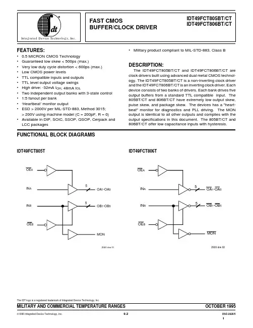
MILITARY AND COMMERCIAL TEMPERATURE RANGESOCTOBER 1995The IDT logo is a registered trademark of Integrated Device Technology, Inc.IDT49FCT805TIDT49FCT806T•0.5 MICRON CMOS Technology•Guaranteed low skew < 500ps (max.)•Very low duty cycle distortion < 600ps (max.)•Low CMOS power levels•TTL compatible inputs and outputs •TTL level output voltage swings •High drive: -32mA I OH , 48mA I OL•Two independent output banks with 3-state control •1:5 fanout per bank•‘Heartbeat’ monitor output•ESD > 2000V per MIL-STD-883, Method 3015;> 200V using machine model (C = 200pF, R = 0)•Available in DIP, SOIC, SSOP, QSOP, Cerpack and LCC packagesAIN AIN BOE BOA 1-OA 5OB 1-OB 5MON2920 drw 01DESCRIPTION:The IDT49FCT805BT/CT and IDT49FCT806BT/CT are clock drivers built using advanced dual metal CMOS technol-ogy. The IDT49FCT805BT/CT is a non-inverting clock driver and the IDT49FCT806BT/CT is an inverting clock driver. Each device consists of two banks of drivers. Each bank drives five output buffers from a standard TTL compatible input. The 805BT/CT and 806BT/CT have extremely low output skew,pulse skew, and package skew. The devices has a "heart-beat" monitor for diagnostics and PLL driving. The MON output is identical to all other outputs and complies with the output specifications in this document. The 805BT/CT and 806BT/CT offer low capacitance inputs with hysteresis.FUNCTIONAL BLOCK DIAGRAMSAIN AIN BOE B-OA 5152920 drw 02PIN CONFIGURATIONSIDT49FCT806TLCC TOP VIEWOB 2OB 3GND OB 4OB 52920 drw 04O E I N I N O E M O 21C1FUNCTION TABLE (1)OB 1OA 1OA 3GND OA 4OA 5OA 2A IN AOB 2OB 3GND OB 4MON IN BOB 5OE B V CC DIP/SOIC/SSOP/QSOP/CERPACKTOP VIEW V CC 2920 drw 03GND 1GND GND IN A23GND 4IN B5B V CC DIP/SOIC/SSOP/QSOP/CERPACKTOP VIEW V CC 2920 drw 051OA 3245OE A LCC TOP VIEW2920 drw 06O E AI N AI N BO E B M O N2920 tbl 021. H = HIGH, L = LOW, Z = High Impedance(1)1. This parameter is measured at characterization but not tested.1.Stresses greater than those listed under ABSOLUTE MAXIMUM RAT-INGS may cause permanent damage to the device. This is a stress rating only and functional operation of the device at these or any other condi-tions above those indicated in the operational sections of this specifica-tion is not implied. Exposure to absolute maximum rating conditions for extended periods may affect reliability. No terminal voltage may exceed V CC by +0.5V unless otherwise noted.2.Input and V CC terminals.3.Output and I/O terminals.NOTES:1.For conditions shown as Max. or Min., use appropriate value specified under Electrical Characteristics for the applicable device type.2.Typical values are at Vcc = 5.0V, +25°C ambient.3.Not more than one output should be tested at one time. Duration of the test should not exceed one second.4.Duration of the condition can not exceed one second.5.The test limit for this parameter is ± 5µA at T A = –55°C.DC ELECTRICAL CHARACTERISTICS OVER OPERATING RANGEFollowing Conditions Apply Unless Otherwise Specified1.For conditions shown as Max. or Min., use appropriate value specified under Electrical Characteristics for the applicable device type.2.Typical values are at V CC = 5.0V, +25°C ambient.3.Per TTL driven input; (V IN = 3.4V); all other inputs at V CC or GND.4.This parameter is not directly testable, but is derived for use in Total Power Supply Calculations.5.Values for these conditions are examples of the I CC formula. These limits are guaranteed but not tested.6.I C = I QUIESCENT + I INPUTS + I DYNAMICI C = I CC + ∆I CC D H N T + I CCD (f O N O)I CC = Quiescent Current (I CCL, I CCH and I CCZ)∆I CC = Power Supply Current for a TTL High Input (V IN = 3.4V)D H = Duty Cycle for TTL Inputs HighN T = Number of TTL Inputs at D HI CCD = Dynamic Current Caused by an Input Transition Pair (HLH or LHL)f O= Output FrequencyN O= Number of Outputs at f OAll currents are in milliamps and all frequencies are in megahertz.(3,4)NOTES:1.See test circuits and waveforms.2.Minimum limits are guaranteed but not tested on Propagation Delays.3.t PLH, t PHL, t SK(t) are production tested. All other parameters guaranteed but not production tested.4.Propagation delay range indicated by Min. and Max. limit is due to V CC, operating temperature and process parameters. These propagation delaylimits do not imply skew.TEST CIRCUITS AND WAVEFORMS TEST CIRCUIT FOR ALL OUTPUTSENABLE AND DISABLE TIMEDEFINITIONS:C L =Load capacitance: includes jig and probe capacitance.R T =Termination resistance: should be equal to Z OUT of the PulseGenerator.2920 lnk 087.0VOUTPUT 1OUTPUT 23V 0V V OH 1.5V 1.5V OL V OH 1.5V OLINPUTt SK(o) = |t PLH2 - t PLH1| or |t PHL2 - t PHL1|3V 1.5V 0V 3.5V0VV OLV OHENABLEDISABLE3V 0V V OH V OL1.5V1.5V3V 0VOH 1.5V 1.5V OL OH 1.5V V OLt SK(t) = |t PLH2 - t PLH1| or |t PHL2 - t PHL1|3V 0VV OH 1.5V 1.5V V OLt SK(p) = |t PHL - t PLH |PULSE SKEW - t SK (p)PACKAGE SKEW - t SK (t)PACKAGE DELAYOUTPUT SKEW- t SK (o)Package 1 and Package 2 are same device type and speed gradeENABLE AND DISABLE TIMES2920 drw 082920 drw 102920 drw 092920 drw 112920 drw 12NOTES:1.Diagram shown for input Control Enable-LOW and input Control Disable-HIGH2.Pulse Generator for All Pulses: f ≤ 1.0MHz; t F ≤ 2.5ns; t R ≤ 2.5nsORDERING INFORMATIONXXXDevice TypeXX XBlank BPDELSO PYQ805BT 806BT 805CT 806CT Commercial (0°C to +70°C)MIL-STD-883, Class B (–55°C to +125°C)Plastic DIPCERDIPCERPACKLeadless Chip CarrierSmall Outline ICShrink Small Outline ICQuarter-size Small Outline PackageNon-Inverting Buffer/Clock DriverInverting Buffer/Clock Driver2920 drw 13 IDT49FCT。
STM8L052C6T6;中文规格书,Datasheet资料
June 2012Doc ID 022924 Rev 21/52STM8L052C6Value Line, 8-bit ultralow power MCU, 32-KB Flash,256-bytes data EEPROM, RTC, LCD, timers,USART, I2C, SPI, ADCData brief target specificationFeatures■Operating conditions–Operating power supply: 1.8 V to 3.6 V –T emperature range: -40 °C to 85 °C ■Low power features– 5 low power modes: Wait, Low power run (5.1µA), Low power wait (3µA), Active-halt with full RTC (1.3µA), Halt (350nA)–Consumption: 195 µA/MHz + 440 µA –Ultra-low leakage per I/0: 50 nA –Fast wakeup from Halt: 4.7 µs■Advanced STM8 core–Harvard architecture and 3-stage pipeline –Max freq. 16 MHz, 16 CISC MIPS peak –Up to 40 external interrupt sources ■Reset and supply management–Low power, ultra-safe BOR reset with 5 selectable thresholds–Ultra low power POR/PDR–Programmable voltage detector (PVD)■Clock management–32 kHz and 1 to 16 MHz crystal oscillator –Internal 16 MHz factory-trimmed RC –Internal 38 kHz low consumption RC –Clock security system■Low power RTC–BCD calendar with alarm interrupt–Auto-wakeup from Halt w/ periodic interrupt ■LCD: up to 4x28 segments w/ step-up converter■Memories–32 KB Flash program memory and256bytes data EEPROM with ECC, RWW –Flexible write and read protection modes – 2 Kbytes of RAM■– 4 channels supporting ADC, SPI, I2C, USART , timers– 1 channel for memory-to-memory ■12-bit ADC up to 1 Msps/25 channels –Internal reference voltage■Timers–T wo 16-bit timers with 2 channels (used as IC, OC, PWM), quadrature encoder–One 16-bit advanced control timer with 3 channels, supporting motor control –One 8-bit timer with 7-bit prescaler– 2 watchdogs: 1 Window, 1 Independent –Beeper timer with 1, 2 or 4 kHz frequencies ■Communication interfaces–Synchronous serial interface (SPI)–Fast I2C 400 kHz SMBus and PMBus –USART (ISO 7816 interface and IrDA)■Up to 41 I/Os, all mappable on interrupt vectors ■Development support–Fast on-chip programming and non- intrusive debugging with SWIM –Bootloader using USARTContents STM8L052C6Contents1Introduction . . . . . . . . . . . . . . . . . . . . . . . . . . . . . . . . . . . . . . . . . . . . . . . . 62Description . . . . . . . . . . . . . . . . . . . . . . . . . . . . . . . . . . . . . . . . . . . . . . . . . 72.1Device overview . . . . . . . . . . . . . . . . . . . . . . . . . . . . . . . . . . . . . . . . . . . . . 82.2Ultra low power continuum . . . . . . . . . . . . . . . . . . . . . . . . . . . . . . . . . . . . . 93Functional overview . . . . . . . . . . . . . . . . . . . . . . . . . . . . . . . . . . . . . . . . 103.1Low power modes . . . . . . . . . . . . . . . . . . . . . . . . . . . . . . . . . . . . . . . . . . 113.2Central processing unit STM8 . . . . . . . . . . . . . . . . . . . . . . . . . . . . . . . . . 123.2.1Advanced STM8 Core . . . . . . . . . . . . . . . . . . . . . . . . . . . . . . . . . . . . . . 123.2.2Interrupt controller . . . . . . . . . . . . . . . . . . . . . . . . . . . . . . . . . . . . . . . . . 123.3Reset and supply management . . . . . . . . . . . . . . . . . . . . . . . . . . . . . . . . 133.3.1Power supply scheme . . . . . . . . . . . . . . . . . . . . . . . . . . . . . . . . . . . . . . 133.3.2Power supply supervisor . . . . . . . . . . . . . . . . . . . . . . . . . . . . . . . . . . . . 133.3.3Voltage regulator . . . . . . . . . . . . . . . . . . . . . . . . . . . . . . . . . . . . . . . . . . 133.4Clock management . . . . . . . . . . . . . . . . . . . . . . . . . . . . . . . . . . . . . . . . . 143.5Low power real-time clock . . . . . . . . . . . . . . . . . . . . . . . . . . . . . . . . . . . . 153.6LCD (Liquid crystal display) . . . . . . . . . . . . . . . . . . . . . . . . . . . . . . . . . . . 163.7Memories . . . . . . . . . . . . . . . . . . . . . . . . . . . . . . . . . . . . . . . . . . . . . . . . . 163.8DMA . . . . . . . . . . . . . . . . . . . . . . . . . . . . . . . . . . . . . . . . . . . . . . . . . . . . . 163.9Analog-to-digital converter . . . . . . . . . . . . . . . . . . . . . . . . . . . . . . . . . . . . 173.10System configuration controller and routing interface . . . . . . . . . . . . . . . 173.11Timers . . . . . . . . . . . . . . . . . . . . . . . . . . . . . . . . . . . . . . . . . . . . . . . . . . . 173.11.1TIM1 - 16-bit advanced control timer . . . . . . . . . . . . . . . . . . . . . . . . . . . 183.11.216-bit general purpose timers . . . . . . . . . . . . . . . . . . . . . . . . . . . . . . . . 183.11.38-bit basic timer . . . . . . . . . . . . . . . . . . . . . . . . . . . . . . . . . . . . . . . . . . . 183.12Watchdog timers . . . . . . . . . . . . . . . . . . . . . . . . . . . . . . . . . . . . . . . . . . . 183.12.1Window watchdog timer . . . . . . . . . . . . . . . . . . . . . . . . . . . . . . . . . . . . . 183.12.2Independent watchdog timer . . . . . . . . . . . . . . . . . . . . . . . . . . . . . . . . . 183.13Beeper . . . . . . . . . . . . . . . . . . . . . . . . . . . . . . . . . . . . . . . . . . . . . . . . . . . 193.14Communication interfaces . . . . . . . . . . . . . . . . . . . . . . . . . . . . . . . . . . . . 193.14.1SPI . . . . . . . . . . . . . . . . . . . . . . . . . . . . . . . . . . . . . . . . . . . . . . . . . . . . . 193.14.2I²C . . . . . . . . . . . . . . . . . . . . . . . . . . . . . . . . . . . . . . . . . . . . . . . . . . . . . 19 2/52Doc ID 022924 Rev 2STM8L052C6Contents3.14.3USART . . . . . . . . . . . . . . . . . . . . . . . . . . . . . . . . . . . . . . . . . . . . . . . . . . 193.15Infrared (IR) interface . . . . . . . . . . . . . . . . . . . . . . . . . . . . . . . . . . . . . . . . 203.16Development support . . . . . . . . . . . . . . . . . . . . . . . . . . . . . . . . . . . . . . . . 204Pin description . . . . . . . . . . . . . . . . . . . . . . . . . . . . . . . . . . . . . . . . . . . . 214.1System configuration options . . . . . . . . . . . . . . . . . . . . . . . . . . . . . . . . . . 265Memory and register map . . . . . . . . . . . . . . . . . . . . . . . . . . . . . . . . . . . 275.1Memory mapping . . . . . . . . . . . . . . . . . . . . . . . . . . . . . . . . . . . . . . . . . . . 275.2Register map . . . . . . . . . . . . . . . . . . . . . . . . . . . . . . . . . . . . . . . . . . . . . . 28 6Interrupt vector mapping . . . . . . . . . . . . . . . . . . . . . . . . . . . . . . . . . . . . 457Package characteristics . . . . . . . . . . . . . . . . . . . . . . . . . . . . . . . . . . . . . 477.1ECOP ACK . . . . . . . . . . . . . . . . . . . . . . . . . . . . . . . . . . . . . . . . . . . . . . . . 477.2Package mechanical data . . . . . . . . . . . . . . . . . . . . . . . . . . . . . . . . . . . . 487.2.148-pin low profile quad flat 7x7mm package (LQFP48) . . . . . . . . . . . . . 48 8Device ordering information . . . . . . . . . . . . . . . . . . . . . . . . . . . . . . . . . . 50 9Revision history . . . . . . . . . . . . . . . . . . . . . . . . . . . . . . . . . . . . . . . . . . . 51Doc ID 022924 Rev 23/52List of tables STM8L052C6 List of tablesTable 1.Medium density value line STM8L05xxx low power device features and peripheral counts 8 Table 2.Timer feature comparison. . . . . . . . . . . . . . . . . . . . . . . . . . . . . . . . . . . . . . . . . . . . . . . . . . 17 Table 3.Legend/abbreviation for Table4. . . . . . . . . . . . . . . . . . . . . . . . . . . . . . . . . . . . . . . . . . . . . 22 Table 4.Medium density value line STM8L05xxx pin description . . . . . . . . . . . . . . . . . . . . . . . . . . 22 Table 5.Flash and RAM boundary addresses. . . . . . . . . . . . . . . . . . . . . . . . . . . . . . . . . . . . . . . . . 28 Table 6.I/O port hardware register map. . . . . . . . . . . . . . . . . . . . . . . . . . . . . . . . . . . . . . . . . . . . . . 28 Table 7.General hardware register map . . . . . . . . . . . . . . . . . . . . . . . . . . . . . . . . . . . . . . . . . . . . . 29 Table 8.CPU/SWIM/debug module/interrupt controller registers. . . . . . . . . . . . . . . . . . . . . . . . . . . 43 Table 9.Interrupt mapping . . . . . . . . . . . . . . . . . . . . . . . . . . . . . . . . . . . . . . . . . . . . . . . . . . . . . . . . 45 Table 10.LQFP48 48-pin low profile quad flat package, mechanical data. . . . . . . . . . . . . . . . . . . . . 48 Table 11.Document revision history . . . . . . . . . . . . . . . . . . . . . . . . . . . . . . . . . . . . . . . . . . . . . . . . . 51 4/52Doc ID 022924 Rev 2STM8L052C6List of figures List of figuresFigure 1.Medium density value line STM8L05xxx device block diagram. . . . . . . . . . . . . . . . . . . . 10 Figure 2.Medium density value line STM8L05xxx clock tree diagram . . . . . . . . . . . . . . . . . . . . . . 15 Figure 3.STM8L052C6 48-pin LQFP48 package pinout (with LCD) . . . . . . . . . . . . . . . . . . . . . . . . 21 Figure 4.Memory map . . . . . . . . . . . . . . . . . . . . . . . . . . . . . . . . . . . . . . . . . . . . . . . . . . . . . . . . . . 27 Figure 5.LQFP48 48-pin low profile quad flat package outline. . . . . . . . . . . . . . . . . . . . . . . . . . . . . 48 Figure 6.LQFP48 recommended footprint . . . . . . . . . . . . . . . . . . . . . . . . . . . . . . . . . . . . . . . . . . . . 49 Figure 7.Medium density value line STM8L05xxx ordering information scheme . . . . . . . . . . . . . . . 50Doc ID 022924 Rev 25/52Introduction STM8L052C66/52Doc ID 022924 Rev 21 I ntroductionThis document describes the features, pinout, mechanical data and ordering information ofthe medium density value line STM8L052C6 microcontroller with 32-Kbyte Flash memory density. For further details on the whole STMicroelectronics medium density family please refer to Section 2.2: Ultra low power continuum .For detailed information on device operation and registers, refer to the reference manual (RM0031).For information on to the Flash program memory and data EEPROM, refer to the programming manual (PM0054).For information on the debug module and SWIM (single wire interface module), refer to the STM8 SWIM communication protocol and debug module user manual (UM0470).For information on the STM8 core, refer to the STM8 CPU programming manual (PM0044).Medium density value line devices provide the following benefits:●Integrated system–32 Kbytes of medium density embedded Flash program memory –256 bytes of data EEPROM – 2 Kbytes of RAM –Internal high speed and low-power low speed RC –Embedded reset ●Ultra low power consumption–195 µA/MHZ + 440 µA (consumption)–0.9 µA with LSI in Active-halt mode –Clock gated system and optimized power management –Capability to execute from RAM for Low power wait mode and low power run mode ●Advanced features–Up to 16 MIPS at 16 MHz CPU clock frequency –Direct memory access (DMA) for memory-to-memory or peripheral-to-memoryaccess● Short development cycles–Application scalability across a common family product architecture withcompatible pinout, memory map and modular peripherals –Wide choice of development tools Refer to T able 1: Medium density value line STM8L05xxx low power device features and peripheral counts and Section 3: Functional overview for an overview of the complete range of peripherals proposed in this family.Figure 1 shows the block diagram of the medium density value line STM8L05xxx family.STM8L052C6Description 2 DescriptionThe medium density value line STM8L05xxx devices are members of the STM8L ultra lowpower 8-bit family.The value line STM8L05xxx ultra low power family features the enhanced STM8 CPU coreproviding increased processing power (up to 16 MIPS at 16 MHz) while maintaining theadvantages of a CISC architecture with improved code density, a 24-bit linear addressingspace and an optimized architecture for low power operations.The family includes an integrated debug module with a hardware interface (SWIM) whichallows non-intrusive In-application debugging and ultra-fast Flash programming.Medium density value line STM8L05xxx microcontrollers feature embedded data EEPROMand low-power, low-voltage, single-supply program Flash memory.All devices offer 12-bit ADC, real-time clock, 16-bit timers, one 8-bit timer as well asstandard communication interface such as SPI, I2C, USART and 4x28-segment LCD. The4x 28-segment LCD is available on the medium density value line STM8L05xxx.The STM8L05xxx family operates from 1.8 V to 3.6 V and is available in the -40 to +85 °Ctemperature range.The modular design of the peripheral set allows the same peripherals to be found in differentST microcontroller families including 32-bit families. This makes any transition to a differentfamily very easy, and simplified even more by the use of a common set of developmenttools.All value line STM8L ultra low power products are based on the same architecture with thesame memory mapping and a coherent pinout.Doc ID 022924 Rev 27/52Description STM8L052C68/52Doc ID 022924 Rev 22.1 Device overviewTable 1.Medium density value line STM8L05xxx low power device features andperipheral countsFeaturesSTM8L052C6Flash (Kbytes)32Data EEPROM (bytes)256RAM (Kbytes)2LCD4x28Timers Basic1 (8-bit)General purpose 2(16-bit)Advanced control 1 (16-bit)CommunicationinterfacesSPI1I2C1USART 1GPIOs41(1)1.The number of GPIOs given in this table includes the NRST/PA1 pin but the application can use theNRST/PA1 pin as general purpose output only (PA1).12-bit synchronized ADC (number of channels) 1 (25)Others RTC, window watchdog, independent watchdog,16-MHz and 38-kHz internal RC,1- to 16-MHz and 32-kHz external oscillatorCPU frequency 16 MHz Operating voltage 1.8 V to 3.6 V Operating temperature -40 to +85 °C PackageLQFP48STM8L052C6DescriptionDoc ID 022924 Rev 29/522.2 Ultra low power continuumThe ultra low power value line STM8L05xxx and STM8L15xxx are fully pin-to-pin, software and feature compatible. Besides the full compatibility within the STM8L family, the devices are part of STMicroelectronics microcontrollers ultra low power strategy which also includes STM8L101xx and STM32L15xxx. The STM8L and STM32L families allow a continuum of performance, peripherals, system architecture, and features.They are all based on STMicroelectronics 0.13µm ultra-low leakage process.Note:1The STM8L05xxx is pin-to-pin compatible with STM8L101xx devices.2The STM32L family is pin-to-pin compatible with the general purpose STM32F family. Please refer to STM32L15x documentation for more information on these devices.PerformanceAll families incorporate highly energy-efficient cores with both Harvard architecture and pipelined execution: advanced STM8 core for STM8L families and ARM Cortex™-M3 core for STM32L family. In addition specific care for the design architecture has been taken to optimize the mA/DMIPS and mA/MHz ratios.This allows the ultra low power performance to range from 5 up to 33.3DMIPs.Shared peripheralsSTM8L05x, STM8L15x and STM32L15xx share identical peripherals which ensure a very easy migration from one family to another:●Analog peripheral: ADC1●Digital peripherals: RTC and some communication interfacesCommon system strategyTo offer flexibility and optimize performance, the STM8L and STM32L devices use a common architecture:●Same power supply range from 1.8 to 3.6V●Architecture optimized to reach ultra-low consumption both in low power modes and Run mode●Fast startup strategy from low power modes ●Flexible system clock●Ultra-safe reset: same reset strategy for both STM8L and STM32L including power-on reset, power-down reset, brownout reset and programmable voltage detectorFeaturesST ultra low power continuum also lies in feature compatibility:●More than 10 packages with pin count from 20 to 100 pins and size down to 3 x 3mm ●Memory density ranging from 4 to 128 KbytesFunctional overview STM8L052C610/52Doc ID 022924 Rev 23 Functional overviewFigure 1.Medium density value line STM8L05xxx device block diagram1.Legend :ADC: Analog-to-digital converter BOR: Brownout resetDMA: Direct memory accessI²C: Inter-integrated circuit multimaster interface LCD: Liquid crystal displayPOR/PDR: Power on reset / power down reset RTC: Real-time clockSPI: Serial peripheral interfaceSWIM: Single wire interface moduleUSART: Universal synchronous asynchronous receiver transmitter WWDG: Window watchdog IWDG: independent watchdog16 MHz internal RC Clock Clocks A d d r e s s , c o n t r o l a n d d a t a b u s e sDebug moduleSPI132 Kbytes Interrupt controller2 Kbytes RAMto core and peripheralsIWDG (38 kHz clock)(SWIM)Port A Port B Port C I²C1USART1PowerVOLT. REG.Port F 1-16 MHz oscillator 32 kHz oscillator 38 kHz internal RC LCD driver 4x28WWDGSTM8 Corecontroller and CSS256 bytes Port D Port E BeeperRTC memoryprogram data EEPROM @V DDV DD18V DD1 =1.8 VV SS1SWIMSCL, SDA,MOSI, MISO, SCK, NSS RX, TX, CKADC1_INxV DDA V SSASMB @V DDA /V SSA12-bit ADC1V REF+V REF-3.6 V NRSTPA[7:0]PB[7:0]PC[7:0]PD[7:0]PE[7:0]PF0BEEPALARM, CALIBSEGx, COMxPOR/PDR OSC_IN,OSC_OUT OSC32_IN,OSC32_OUTto BOR PVDPVD_INRESET DMA18-bit Timer 416-bit Timer 3 16-bit Timer 2 16-bit Timer 1 (4 channels)2 channels 2 channels3 channelsV LCD = 2.5 V 3.6 VtoLCD boosterInternal referencevoltageVREFINT outInfrared interface IR_TIM分销商库存信息: STMSTM8L052C6T6。
NT805-552T中文资料
元器件交易网
ROMOLAND, INC.
SINGLE PORT NT805-XXXT SERIES
TRANSFORMER, LAN, SMD 10/100 BASE-TX
February 27, 2004
PACKAGE 1
d DATATRONICS NT805-XXXT XXXX
Loss dB Max
1-100 MHz
-1 -1 -1 -1
-1 -1 -1 -1 -1 -1 -1 -1 -1 -1 -1 -1 -1 -1 -1 -1.1 -1.1 -1.1 -1.1 -1.1
30 MHz
-42 -42 -42 -42 -42 -42 -42 -42 -42 -42 -42 -42 -42 -42 -42 -42 -42 -42 -42 -42 -42 -42 -42 -42
10
1
7
2
9
3
8
TRANSMIT CHANNEL
16
16
10
15
13
11
15 12
9
Datatronics: 28151 Highway 74, Romoland, CA 92585 Tel: 951-928-7700 Toll Free Tel: 888-889-5391 Fax: 951-928-7701 Email: drisales@
CIRCUIT 2
1
2 3
TRANSMIT CHANNEL
14
7 15
5
6 16
7 6 8 RECEIVE CHANNEL
TRANSMIT CHANNEL 11 12 10
CIRCUIT 4
11
9 10
805OPM Module Datasheet说明书
Design specifications• T ransient voltage suppression: EN6100-6-1.• P CB characteristics: UL 94V-0.• P ower distribution: UL 1077 compliant(except high-voltage dielectric test).• Load dump tested to ISO 16750-2.Key features• 8 channels with outputs capable of up to 15 ampseach (no more than 50 amps continuously for the module).• P airs of channels may be configured to operate inparallel.• P WM dimming capability on all channels.• Input capability on all channels.• R everse battery protected.• S tatus LEDs for each channel.• T hermal, short circuit, and programmable overloadprotection.• L ocal manual override capabilities.• D esigned for motor and high inrush current loads.• E-Plex LEN value 2.Octal Power Module8 channel DC power distribution moduleElectrical specificationsNOTES:1. Module will shut down when voltage reaches 8.5 V and will power back up at 9 V2. Specified as 50 feet of 2 AWG (43 mm²) wires with a 6 inch diameter spool for both power and ground.3. Refer to maximum load inductance graph belowTaking the device outside the limits specified above may cause permanent damage to the device.The supply to the module should be protected by a fuse or circuit breaker of appropriate capacity and no more than a maximum capacity of 50 A.Trip spee d charact eristicsMaximum load inductanceE-Plex activity LEDE-Plex address indicationManual modeAt power up the module will indicate its E-Plex address by flashing the LEDs. One of the LEDs will flash for 2 seconds, this indicates the most significant digit of the address. This will be followed by one second with all LEDs off. Then another LED will flash to indicate the next digit of the address. This pattern will repeat until all 4 digits have been displayed. For example if LED 1 flashes followed by LED 6, then fault (0), then 8, the modules address is 1608.All LEDs flash repeatedly with the above sequence at power up if the module has not been assigned an address.Manual mode is a backup mode of operation which is automatically enabled if no commands are received from the main control unit (clock module). This allows for a minimum level of device control even when there are faults with other parts of the system.If a module is unprogrammed all channels are disabled.When the network is inactive there are two parameters that may be configured for output channels; automatic and manual control.Automatic controlWhen automatic control is enabled the channel can be set to turn its output on or off when the module enters manual mode. When disabled the output will remain in the same state as it was in before entering manual mode.Manual controlThe keypad switches may be programmed to override the automatic control with either momentary or latching behaviour.When the network is active the functionality of the buttons is determined by the system software.Typical wiring diagramNav equipmentHalogen lightingCable sizingFor Power / Battery ConnectionsMust be protected at a maximum of 50 A. Maximum wire size should be sized based on upstream fuse capacity. When connecting the power source to the power studs on the module, the M5 hex nuts should be torqued to 3 Nm (22 in lb) after installing the battery terminals to the studs. Failure to properly torque hex nuts may result damage to the unit and intermittent operation due to terminals loosening over time.When using a single conductor, a 35 mm² cable with a typical ring terminal thickness can be used. When using two conductors, 25 mm² cable with typical ring terminal thickness can be used. At least one turn of thread must be visible over the nut after tightening. It is important not to fit a washer below the ring terminal as the increased resistance will cause heating and damage to the module and cabling.Parallel OperationWhen connecting channels in parallel, it is important to match the resistance of the wires from each channel. If the wires are not balanced, one will carry more current than the other, which may result in the channel tripping prematurely.The best way to ensure that the wires are matched is to join them as close to the module a possible using wires of equal length and cross sectional area. This should be 4 mm² (14 AWG) wire, no longer than 100 mm (4”). E-Plex Ltd. can supply a pre-made assembly for this purpose. See below for the ordering code.Loads with multiple suppliesWhen a channel is used to power a load, it is necessary to fit a back feed prevention diode to protect against equipment damage when the OPM channel is off but the other channel is on. E-Plex Ltd. can supply a back feed diode with integral resister which will protect against back feeding whilst still allowing feedback to be monitored. See below for the ordering code.DimensionsMounting instructionsScrew assembly to a flat mounting surface in two places, as shown in the illustration labels A and B. Use M4 size panhead screw, M4 split lock washer and M4 washer or No. 6 wood screw Torque to 250~280 N-cm. Do not exceed this torque as it could cause damage to the enclosure.The 805OPM device can be supplied as a retro fit module and will have the relevant firmware personality for the older module it is replacing.These modules are the 366HMM, 407QHM, 413DWM 4 when ordered (see part number below) they will require the relevant adapter cable to allow it to be connected to the original wiring. Due to the size of the 805OPM module vs the older modules a diagram showing module and cable space requirements is shown below.The personality in the 805OPM module makes the system believe that the original module type is connected and the programming and responses will be the same.For information on specification changes and connections an additional information sheet is available and provided with the supplied module.NOTES:3It is not recommended to use emulated devices for new installs and only as necessary for retrofits.We would always recommend using the native 805OPM for future compatibility and upgradability.4When emulating a 413DWM, additional external diodes may be required, depending on application. If in doubt, please contact your local dealer.805OPM Retrofit and personalities 3Mechanical specificationsNOTES:1. Outputs shut down at 80ºC and come back on at 75ºC.Dimensioned Drawing with retro fit cable fittedOrdering codesWhen used as emulated device type805OPM Version 1.0 | AUG 2018 email:***************.ukImportant Notice: E-Plex Ltd. (E-Plex) reserves the right to make changes to or discontinue any product or service identified in this publication without notice. E-Plex advises its customers to obtain the latest version of the relevant information to verify, before placing any orders, that the information being relied upon is current. E-Plex assumes no responsibility for infringement of patents or rights of others based on E-Plex applications assistance or product specifications since E-Plex does not possess full access concerning the use or application of customers’ products. E-Plex also assumes no responsibility for customers’ product designs.。
795S中文资料
1/32April 2006STM690, STM704, STM795STM802, STM804, STM805, STM8063V Supervisor with Battery Switchover* Contact local ST sales office for availability.Rev 7FEATURES SUMMARY■■NVRAM SUPERVISOR FOR EXTERNAL LPSRAM■CHIP-ENABLE GATING (STM795 only) FOR EXTERNAL LPSRAM (7ns max PROP DELAY)■MANUAL (PUSH-BUTTON) RESET INPUT ■200ms (TYP) t rec■WATCHDOG TIMER - 1.6sec (TYP)■AUTOMATIC BATTERY SWITCHOVER■LOW BATTERY SUPPLY CURRENT - 0.4µA (TYP)■POWER-FAIL COMPARATOR (PFI/PFO)■LOW SUPPLY CURRENT - 40µA (TYP)■GUARANTEED RST (RST) ASSERTION DOWN TO V CC = 1.0V■OPERATING TEMPERATURE:–40°C to 85°C (Industrial Grade)Table 1. Device OptionsNote: 1.2.Open drain output.Watchdog InputActive- Low RST (1)Active- High RSTManual Reset Input Battery Switch-overPower-fail Compar-atorChip-Enable GatingSTM690T/S/R ✔✔✔✔STM704T/S/R ✔✔✔✔STM795T/S/R ✔(2)✔✔STM802T/S/R ✔✔✔✔STM804T/S/R ✔✔(2)✔✔STM805T/S/R ✔✔(2)✔✔STM806T/S/R✔✔✔✔STM690/704/795/802/804/805/806TABLE OF CONTENTSFEATURES SUMMARY . . . . . . . . . . . . . . . . . . . . . . . . . . . . . . . . . . . . . . . . . . . . . . . . . . . . . . . . . . . . .1Figure 1.Packages. . . . . . . . . . . . . . . . . . . . . . . . . . . . . . . . . . . . . . . . . . . . . . . . . . . . . . . . . . . . . .1 Table 1.Device Options . . . . . . . . . . . . . . . . . . . . . . . . . . . . . . . . . . . . . . . . . . . . . . . . . . . . . . . . .1SUMMARY DESCRIPTION. . . . . . . . . . . . . . . . . . . . . . . . . . . . . . . . . . . . . . . . . . . . . . . . . . . . . . . . . . .4Figure 2.Logic Diagram (STM690/802/804/805) . . . . . . . . . . . . . . . . . . . . . . . . . . . . . . . . . . . . . . .4 Figure 3.Logic Diagram (STM704/806) . . . . . . . . . . . . . . . . . . . . . . . . . . . . . . . . . . . . . . . . . . . . . .4 Figure 4.Logic Diagram (STM795). . . . . . . . . . . . . . . . . . . . . . . . . . . . . . . . . . . . . . . . . . . . . . . . . .4 Table 2.Signal Names . . . . . . . . . . . . . . . . . . . . . . . . . . . . . . . . . . . . . . . . . . . . . . . . . . . . . . . . . .4 Figure 5.STM690/802/804/805 Connections. . . . . . . . . . . . . . . . . . . . . . . . . . . . . . . . . . . . . . . . . .5 Figure 6.STM704/806 Connections. . . . . . . . . . . . . . . . . . . . . . . . . . . . . . . . . . . . . . . . . . . . . . . . .5 Figure 7.STM795 Connections . . . . . . . . . . . . . . . . . . . . . . . . . . . . . . . . . . . . . . . . . . . . . . . . . . . .5 Pin Descriptions . . . . . . . . . . . . . . . . . . . . . . . . . . . . . . . . . . . . . . . . . . . . . . . . . . . . . . . . . . . . . . .6 Table 3.Pin Description. . . . . . . . . . . . . . . . . . . . . . . . . . . . . . . . . . . . . . . . . . . . . . . . . . . . . . . . . .6 Figure 8.Block Diagram (STM690/802/804/805). . . . . . . . . . . . . . . . . . . . . . . . . . . . . . . . . . . . . . .7 Figure 9.Block Diagram (STM704/806). . . . . . . . . . . . . . . . . . . . . . . . . . . . . . . . . . . . . . . . . . . . . .7 Figure 10.Block Diagram (STM795) . . . . . . . . . . . . . . . . . . . . . . . . . . . . . . . . . . . . . . . . . . . . . . . . .8 Figure 11.Hardware Hookup. . . . . . . . . . . . . . . . . . . . . . . . . . . . . . . . . . . . . . . . . . . . . . . . . . . . . . .8OPERATION . . . . . . . . . . . . . . . . . . . . . . . . . . . . . . . . . . . . . . . . . . . . . . . . . . . . . . . . . . . . . . . . . . . . . .9Reset Output . . . . . . . . . . . . . . . . . . . . . . . . . . . . . . . . . . . . . . . . . . . . . . . . . . . . . . . . . . . . . . . . . .9 Push-button Reset Input (STM704/806). . . . . . . . . . . . . . . . . . . . . . . . . . . . . . . . . . . . . . . . . . . . .9 Watchdog Input (NOT available on STM704/795/806) . . . . . . . . . . . . . . . . . . . . . . . . . . . . . . . . .9 Back-up Battery Switchover. . . . . . . . . . . . . . . . . . . . . . . . . . . . . . . . . . . . . . . . . . . . . . . . . . . . . .9 Table 4.I/O Status in Battery Back-up . . . . . . . . . . . . . . . . . . . . . . . . . . . . . . . . . . . . . . . . . . . . ..9 Chip-Enable Gating (STM795 only) . . . . . . . . . . . . . . . . . . . . . . . . . . . . . . . . . . . . . . . . . . . . . . .10 Chip Enable Input (STM795 only). . . . . . . . . . . . . . . . . . . . . . . . . . . . . . . . . . . . . . . . . . . . . . . . .10 Chip Enable Output (STM795 only) . . . . . . . . . . . . . . . . . . . . . . . . . . . . . . . . . . . . . . . . . . . . . . .10 Figure 12.Chip-Enable Gating. . . . . . . . . . . . . . . . . . . . . . . . . . . . . . . . . . . . . . . . . . . . . . . . . . . . .10 Figure 13.Chip Enable Waveform (STM795) . . . . . . . . . . . . . . . . . . . . . . . . . . . . . . . . . . . . . . . . .10 Power-fail Input/Output (NOT available on STM795) . . . . . . . . . . . . . . . . . . . . . . . . . . . . . . . . .11 Applications Information . . . . . . . . . . . . . . . . . . . . . . . . . . . . . . . . . . . . . . . . . . . . . . . . . . . . . . .11 Figure 14.Power-fail Comparator Waveform (STM690/704/802/804/805/806). . . . . . . . . . . . . . . .11 Using a SuperCap™ as a Backup Power Source. . . . . . . . . . . . . . . . . . . . . . . . . . . . . . . . . . . .12 Figure ing a SuperCap™. . . . . . . . . . . . . . . . . . . . . . . . . . . . . . . . . . . . . . . . . . . . . . . . . . . .12 Negative-Going V CC Transients. . . . . . . . . . . . . . . . . . . . . . . . . . . . . . . . . . . . . . . . . . . . . . . . . .12TYPICAL OPERATING CHARACTERISTICS . . . . . . . . . . . . . . . . . . . . . . . . . . . . . . . . . . . . . . . . . . .13Figure 16.V CC-to-V OUT On-Resistance vs. Temperature . . . . . . . . . . . . . . . . . . . . . . . . . . . . . . . .13 Figure 17.V BAT-to-V OUT On-Resistance vs. Temperature. . . . . . . . . . . . . . . . . . . . . . . . . . . . . . . .13 Figure 18.Supply Current vs. Temperature (no load) . . . . . . . . . . . . . . . . . . . . . . . . . . . . . . . . . . .14 Figure 19.Battery Current vs. Temperature. . . . . . . . . . . . . . . . . . . . . . . . . . . . . . . . . . . . . . . . . . .14 Figure 20.V PFI Threshold vs. Temperature. . . . . . . . . . . . . . . . . . . . . . . . . . . . . . . . . . . . . . . . . . .152/32STM690/704/795/802/804/805/806Figure 21.Reset Comparator Propagation Delay vs. Temperature. . . . . . . . . . . . . . . . . . . . . . . . .15 Figure 22.Power-up t rec vs. Temperature . . . . . . . . . . . . . . . . . . . . . . . . . . . . . . . . . . . . . . . . . . . .16 Figure 23.Normalized Reset Threshold vs. Temperature . . . . . . . . . . . . . . . . . . . . . . . . . . . . . . . .16 Figure 24.Watchdog Time-out Period vs. Temperature . . . . . . . . . . . . . . . . . . . . . . . . . . . . . . . . .17 Figure 25.E to E CON On-Resistance vs. Temperature . . . . . . . . . . . . . . . . . . . . . . . . . . . . . . . . . .1718 Figure 27.Output Voltage vs. Load Current (V CC = 5V; V BAT = 2.8V; T A = 25°C). . . . . . . . . . . . . .18 Figure 28.Output Voltage vs. Load Current (V CC = 0V; V BAT = 2.8V; T A = 25°C). . . . . . . . . . . . . .19 Figure 29.RST Output Voltage vs. Supply Voltage. . . . . . . . . . . . . . . . . . . . . . . . . . . . . . . . . . . . .19 Figure 30.RST Output Voltage vs. Supply Voltage. . . . . . . . . . . . . . . . . . . . . . . . . . . . . . . . . . . . .20 Figure 31.Power-fail Comparator Response Time (Assertion) . . . . . . . . . . . . . . . . . . . . . . . . . . . .20 Figure 32.Power-fail Comparator Response Time (De-Assertion) . . . . . . . . . . . . . . . . . . . . . . . . .21 Figure 33.Maximum Transient Duration vs. Reset Threshold Overdrive. . . . . . . . . . . . . . . . . . . . .21 CON Propagation Delay vs. Temperature . . . . . . . . . . . . . . . . . . . . . . . . . . . . . . .22MAXIMUM RATING. . . . . . . . . . . . . . . . . . . . . . . . . . . . . . . . . . . . . . . . . . . . . . . . . . . . . . . . . . . . . . . .22 Table 5.Absolute Maximum Ratings. . . . . . . . . . . . . . . . . . . . . . . . . . . . . . . . . . . . . . . . . . . . . . .22DC and AC PARAMETERS . . . . . . . . . . . . . . . . . . . . . . . . . . . . . . . . . . . . . . . . . . . . . . . . . . . . . . . . .23Table 6.Operating and AC Measurement Conditions. . . . . . . . . . . . . . . . . . . . . . . . . . . . . . . . . .2323 Figure 36.AC Testing Input/Output Waveforms. . . . . . . . . . . . . . . . . . . . . . . . . . . . . . . . . . . . . . . .23 Figure 37.MR Timing Waveform . . . . . . . . . . . . . . . . . . . . . . . . . . . . . . . . . . . . . . . . . . . . . . . . . . .24 Figure 38.Watchdog Timing . . . . . . . . . . . . . . . . . . . . . . . . . . . . . . . . . . . . . . . . . . . . . . . . . . . . . .24 Table 7.DC and AC Characteristics . . . . . . . . . . . . . . . . . . . . . . . . . . . . . . . . . . . . . . . . . . . . . . .24PACKAGE MECHANICAL . . . . . . . . . . . . . . . . . . . . . . . . . . . . . . . . . . . . . . . . . . . . . . . . . . . . . . . . . .27Figure 39.SO8 – 8-lead Plastic Small Outline, 150 mils body width, Package Mech. Drawing. . . .27 Table 8.SO8 – 8-lead Plastic Small Outline, 150 mils body width, Package Mechanical Data . .27 Figure 40.TSSOP8 – 8-lead, Thin Shrink Small Outline, 3x3mm body size, Outline . . . . . . . . . . .28 Table 9.TSSOP8 – 8-lead, Thin Shrink Small Outline, 3x3mm body size, Mechanical Data. . . .28PART NUMBERING . . . . . . . . . . . . . . . . . . . . . . . . . . . . . . . . . . . . . . . . . . . . . . . . . . . . . . . . . . . . . . .29Table 10.Ordering Information Scheme . . . . . . . . . . . . . . . . . . . . . . . . . . . . . . . . . . . . . . . . . . . . .29 Table 11.Marking Description. . . . . . . . . . . . . . . . . . . . . . . . . . . . . . . . . . . . . . . . . . . . . . . . . . . . .30REVISION HISTORY. . . . . . . . . . . . . . . . . . . . . . . . . . . . . . . . . . . . . . . . . . . . . . . . . . . . . . . . . . . . . . .31 Table 12.Document Revision History. . . . . . . . . . . . . . . . . . . . . . . . . . . . . . . . . . . . . . . . . . . . . . .313/32STM690/704/795/802/804/805/8064/32SUMMARY DESCRIPTIONThe STM690/704/795/802/804/805/806 Supervi-sors are self-contained devices which provide mi-croprocessor supervisory functions with the ability to non-volatize and write-protect external LPSRAM. A precision voltage reference and com-parator monitors the V CC input for an out-of-toler-ance condition. When an invalid V CC condition occurs, the reset output (RST) is forced low (or high in the case of RST). These devices also offer a watchdog timer (except for STM704/795/806) as well as a power-fail comparator (except for STM795) to provide the system with an early warning of impending power failure.These devices are available in a standard 8-pin SOIC package or a space-saving 8-pin TSSOP package.Note: 1.For STM804/805, reset output is active-high and opendrain.Table 2. Signal NamesNote: 1.Open drain for STM804/805 only.2.STM795MR Push-button Reset Input WDIWatchdog InputRST Active-Low Reset Output RST (1)Active-High Reset Output E (2)Chip Enable InputE CON (2)Conditioned Chip Enable Output Vccsw (2)V CC Switch Output V OUTSupply Voltage Output V CC Supply Voltage V BAT Back-up Supply Voltage PFI Power-fail Input PFO Power-fail Output V SSGroundSTM690/704/795/802/804/805/806drain.5/32STM690/704/795/802/804/805/8066/32Pin DescriptionsMR (Manual Reset).A logic low on /MR assertsthe reset output. Reset remains asserted as long as MR is low and for t rec after MR returns high.This active-low input has an internal pull-up. It can be driven from a TTL or CMOS logic line, or short-ed to ground with a switch. Leave open if unused.WDI (Watchdog Input).If WDI remains high orlow for 1.6sec, the internal watchdog timer runsout and reset is triggered. The internal watchdogtimer clears while reset is asserted or when WDIsees a rising or falling edge.The watchdog function cannot be disabled by al-lowing the WDI pin to float.Pulses low for t recwhen triggered, and stays low whenever V CC islow. It remains low for t rec after either V CC risesabove the reset threshold, the watchdog triggers areset, or MR goes from low to high.RST (Active-high Reset - Open Drain).Pulseshigh for t rec when triggered, and stays high when-ever V CC is above the reset threshold or when MRis a logic high. It remains high for t rec after eitherV CC falls below the reset threshold, the watchdogtriggers a reset, or MR goes from high to low.PFI (Power-fail Input).When PFI is less thanV PFI or when V CC falls below V SW to ground if unused.PFO (Power-fail Output).When PFI is less than V PFI , or V CC falls below V SW , PFO goes low; oth-erwise, PFO remains high. Leave open if unused.V OUT (Supply Output Voltage).When V CC is above the switchover voltage (V SO ), V OUT is con-nected to V CC through a P-channel MOSFET switch. When V CC falls below V SO , V BAT connects to V OUT . Connect to V CC if no battery is Switch Output).When V OUT switches to battery, Vccsw is high. When V OUT switches back to V CC to drive gate of external PMOS transistor for I OUT requirements exceeding 75mA.The input to the chip-en-able gating circuit. Connect to ground if unused.E CON (Conditional Chip Enable).E CON goes low only when E is low and reset is not asserted. If E CON is low when reset is asserted, E CON will re-main low for 15µs or until E goes high, whichever occurs first. In the disabled mode, E CON is pulled up to V OUT .V BAT (Back-up Battery Input).When V CC falls below V SO , V OUT switches from V CC to V BAT .When V CC rises above V SO + hysteresis, V OUT re-connects to V CC . V BAT may exceed V CC . Connect to V CC if no battery is used.Table 3. Pin DescriptionPinNameFunctionSTM795STM690STM802STM704STM806STM804STM805––6–MR Push-button Reset Input –6–6WDI Watchdog Input777–RST Active-Low Reset Output –––7RST Active-High ResetOutput –444PFI Power-failInput –555PFO Power-fail Output1111V OUT Supply Output for External LPSRAM 2222V CC Supply Voltage 3–––Vccsw V CC Switch Output 4333V SS Ground5–––E Chip Enable Input6–––E CON Conditioned Chip Enable Output 8888V BATBackup-Battery InputSTM690/704/795/802/804/805/806Note: 1.For STM804/805, reset output is active-high and open drain.7/32STM690/704/795/802/804/805/806Note: 1.For STM690/802/804/805.2.For STM795 only.3.Not available on STM795.4.For STM704/806.8/32STM690/704/795/802/804/805/806 OPERATIONReset OutputThe STM690/704/795/802/804/805/806 Supervi-sor asserts a reset signal to the MCU whenever V CC goes below the reset threshold (V RST), a watchdog time-out occurs, or when the Push-but-teed to be a logic low (logic high for STM804/805) for 0V < V CC < V RST if V BAT is greater than 1V. id down to V CC =1V.During power-up, once V CC exceeds the reset threshold an internal timer keeps RST low for the reset time-out period, t recreturns high.If V CC drops below the reset threshold, RST goes low. Each time RST is asserted, it stays low for at least the reset time-out period (t rec). Any time V CC goes below the reset threshold the internal timer clears. The reset timer starts when V CC returns above the reset threshold.Push-button Reset Input (STM704/806)A logic low on MR asserts reset. Reset remainsrec (see Figure 37.,page24) after it returns high. The MR input has an internal 40kΩ pull-up resistor, allowing it to be left open if not used. This input can be driven with TTL/CMOS-logic levels or with open-drain/ collector outputs. Connect a normally open mo-mentary switch from MR to GND to create a man-ual reset function; external debounce circuitry is not required. If MR is driven from long cables or the device is used in a noisy environment, connect a 0.1µF capacitor from MR to GND to provide ad-ditional noise immunity. MR may float, or be tied to V CC when not used.Watchdog Input (NOT available on STM704/ 795/806)The watchdog timer can be used to detect an out-of-control MCU. If the MCU does not toggle the Watchdog Input (WDI) within t WD (1.6sec typ), the reset is asserted. The internal watchdog timer is cleared by either:1. a reset pulse, or2.by toggling WDI (high-to-low or low-to-high),which can detect pulses as short as 50ns. If WDI is tied high or low, a reset pulse istriggered every 1.8sec (t WD + t rec).The timer remains cleared and does not count for as long as reset is asserted. As soon as reset is re-leased, the timer starts counting (see Figure 38.,page24).Note: Input frequency greater than 20ns (50MHz) will be filtered.Back-up Battery SwitchoverIn the event of a power failure, it may be necessary to preserve the contents of external SRAM through V OUT. With a backup battery installed with voltage V BAT, the devices automatically switch the SRAM to the back-up supply when V CC falls. Note: If back-up battery is not used, connect both V BAT and V OUT to V CC.This family of Supervisors does not always con-nect V BAT to V OUT when V BAT is greater than V CC. V BAT connects to V OUT (through a 100Ω switch) when V CC is below V SW (2.4V) or V BAT (whichever is lower). This is done to allow the back-up battery (e.g., a 3.6V lithium cell) to have a higher voltage than V CC.Assuming that V BAT > 2.0V, switchover at V SO en-sures that battery back-up mode is entered before V OUT gets too close to the 2.0V minimum required to reliably retain data in most external SRAMs. When V CC recovers, hysteresis is used to avoid oscillation around the V SO point. V OUT is connect-ed to V CC through a 3Ω PMOS power switch. Note: The back-up battery may be removed while V CC is valid, assuming V BAT is adequately decou-pled (0.1µF typ), without danger of triggering a re-set.Table 4. I/O Status in Battery Back-up Pin StatusV OUT Connected to V BAT through internal switchV CC Disconnected from V OUTPFI DisabledPFO Logic LowE High impedanceE CON Logic HighWDI Watchdog timer is disabledMR DisabledRST Logic LowRST Logic HighV BAT Connected to V OUTVccsw Logic High (STM795)9/32STM690/704/795/802/804/805/80610/32Chip-Enable Gating (STM795 only)vents erroneous data from corrupting the external CMOS RAM in the event of an undervoltage con-dition. The STM795 uses a series transmission CON (see Figure 12). During nor-mal operation (reset not asserted), the E transmis-sion gate is enabled and passes all E transitions.When reset is asserted, this path becomes dis-abled, preventing erroneous data from corrupting the CMOS RAM. The short E propagation delay from E to E CON enables the STM795 to be used with most µPs. If E is low when reset asserts,CON remains low for typically 10µs to permit the current WRITE cycle to complete.Chip Enable Input (STM795 only)The chip-enable transmission gate is disabled and is asserted. During a power-down sequence when V CC passes the reset threshold, the chip-enable transmission gate disables and E immediately be-comes high impedance if the voltage at E is high.If E is low when reset asserts, the chip-enable transmission gate will disable 10µs after reset as-serts (see Figure 13). This permits the current WRITE cycle to complete during power-down.Any time a reset is generated, the chip-enable transmission gate remains disabled and E remains first half of the reset time-out period (t rec /2). When the chip enable transmission gate is enabled, the impedance of E appears as a 40Ω resistor in se-ries with the load at E CON . The propagation delay through the chip-enable transmission gate de-pends on V CC , the source impedance of the drive connected to E, and the loading on E CON . The chip enable propagation delay is production tested from the 50% point on E to the 50% point on E CON using a 50Ω driver and a 50pF load capacitance (see Figure 36.,page 23). For minimum propaga-CON and use a low-output impedance driver.Chip Enable Output (STM795 only)When the chip-enable transmission gate is en-CON is equivalent to a 40Ωthe disabled mode, the transmission gate is off and an active pull-up connects E CON to V OUT (see Figure 12). This pull-up turns off when the trans-mission gate is enabled.Power-fail Input/Output (NOT available on STM795)The Power-fail Input (PFI) is compared to an inter-nal reference voltage (independent from the V RST comparator). If PFI is less than the power-fail threshold (V PFI), the Power-Fail Output (PFO) will go low. This function is intended for use as an un-dervoltage detector to signal a failing power sup-ply. Typically PFI is connected through an external voltage divider (see Figure 11.,page8) to either the unregulated DC input (if it is available) or the regulated output of the V CC regulator. The voltage divider can be set up such that the voltage at PFI falls below V PFI several milliseconds before the regulated V CC input to the STM690/704/795/802/ 804/805/806 or the microprocessor drops below the minimum operating voltage.During battery back-up, the power-fail comparator Figure 14.,page11). This occurs after V CC drops below V SW (2.4V). When power returns, the pow-If the comparator is unused, PFI should be con-nected to V SS and PFO left unconnected. PFO may be connected to MR on the STM704/806 so that a low voltage on PFI will generate a reset out-put.Applications InformationThese Supervisor circuits are not short-circuit pro-tected. Shorting V OUT to ground - excluding pow-er-up transients such as charging a decoupling capacitor - destroys the device. Decouple both V CC and V BAT pins to ground by placing 0.1µF ca-pacitors as close to the device as possible.11/32Using a SuperCap™ as a Backup Power SourceSuperCaps™ are capacitors with extremely high capacitance values (e.g., order of 0.47F) for their size. Figure 15 shows how to use a SuperCap as a back-up power source. The SuperCap may be connected through a diode to the V CC supply. Since V BAT can exceed V CC while V CC is above the reset threshold, there are no special precau-tions when using these supervisors with a Super-Cap.Negative-Going V CC TransientsThe STM690/704/795/802/804/805/806 Supervi-sors are relatively immune to negative-going V CC transients (glitches). Figure 33.,page21 was gen-erated using a negative pulse applied to V CC, starting at V RST + 0.3V and ending below the reset threshold by the magnitude indicated (comparator overdrive). The graph indicates the maximum pulse width a negative V CC transient can have without causing a reset pulse. As the magnitude of the transient increases (further below the thresh-old), the maximum allowable pulse width decreas-es. Any combination of duration and overdrive which lies under the curve will NOT generate a re-set signal. Typically, a V CC transient that goes 100mV below the reset threshold and lasts 40µs or less will not cause a reset pulse. A 0.1µF bypass capacitor mounted as close as possible to the V CC pin provides additional transient immunity.12/32TYPICAL OPERATING CHARACTERISTICSNote: Typical values are at T A = 25°C.13/3214/3215/3216/32Figure 25. E to E17/32Figure 26. PFI to PFO Propagation Delay vs. Temperature18/32Figure 29. RST Output Voltage vs. Supply Voltage19/32500ns/divAI09153b20/32Figure 33. Maximum Transient Duration vs. Reset Threshold Overdrive AI09154b500ns/div21/3222/32Figure 34. E to E MAXIMUM RATINGStressing the device above the rating listed in the Absolute Maximum Ratings” table may cause per-manent damage to the device. These are stress ratings only and operation of the device at these or any other conditions above those indicated in the Operating sections of this specification is not im-plied. Exposure to Absolute Maximum Rating con-ditions for extended periods may affect device reliability. Refer also to the STMicroelectronics SURE Program and other relevant quality docu-ments.Table 5. Absolute Maximum RatingsNote: 1.Reflow at peak temperature of 255°C to 260°C for < 30 seconds (total thermal budget not to exceed 180°C for between 90 to 150seconds).Symbol ParameterValue Unit T STG Storage Temperature (V CC Off)–55 to 150°C T SLD (1)Lead Solder Temperature for 10 seconds 260°C V IO Input or Output Voltage –0.3 to V CC +0.3V V CC /V BATSupply Voltage –0.3 to 6.0V I O Output Current 20mA P DPower Dissipation320mW23/32DC AND AC PARAMETERSThis section summarizes the operating measure-ment conditions, and the DC and AC characteris-tics of the device. The parameters in the DC and AC characteristics Tables that follow, are derived from tests performed under the MeasurementConditions summarized in Table 6, Operating and AC Measurement Conditions. Designers should check that the operating conditions in their circuit match the operating conditions when relying on the quoted parameters.Table 6. Operating and AC Measurement ConditionsFigure 35. E to E Note: 1.C L includes load capacitance and scope probe capacitance.ParameterSTM690/704/795/802/804/805/806Unit V CC /V BAT Supply Voltage1.0 to 5.5V Ambient Operating Temperature (T A )–40 to 85°C Input Rise and Fall Times ≤5ns Input Pulse Voltages0.2 to 0.8V CC V Input and Output Timing Ref. Voltages0.3 to 0.7V CCVFigure 37. MR Timing Waveform Note: 1.RST for STM805.Table 7. DC and AC CharacteristicsSym Alter-nativeDescription Test Condition(1)Min Typ Max UnitV CC,V BAT(2)Operating Voltage T A = –40 to +85°C 1.1(3) 5.5VI CC V CC Supply CurrentExcluding I OUT (V CC < 5.5V)4060µAExcluding I OUT (V CC < 3.6V)3550µA V CC Supply Current inBattery Back-up ModeExcluding I OUT(V BAT = 2.3V,V CC = 2.0V, MR = V CC)2535µAI BAT(4)V BAT Supply Current inBattery Back-up ModeExcluding I OUT(V BAT = 3.6V)0.4 1.0µAV OUT1V OUT Voltage (Active)I OUT1 = 5mA(5)V CC –0.03V CC –0.015V I OUT1 = 75mAV CC –0.3V CC –0.15V I OUT1 = 250µA,V CC > 2.5V(5)V CC –0.0015V CC –0.0006VV OUT2V OUT Voltage (BatteryBack-up)I OUT2 = 250µA, V BAT = 2.3VV BAT –0.1V BAT –0.034VI OUT2 = 1mA, V BAT = 2.3VV BAT –0.14V V CC to V OUT On-resistance34ΩV BAT to V OUT On-resistance100Ω24/32I LI Input Leakage Current (MR)STM704/806 only;MR = 0V, V CC = 3V2075350µA Input Leakage Current (PFI)0V = V IN = V CC–252+25nA Input Leakage Current (WDI)0V = V IN = V CC–1+1µAI LO Output Leakage Current STM804/805/795;0V = V IN = V CC(6)–1+1µAV IH Input High Voltage (MR, WDI)V RST (max) < V CC < 5.5V0.7V CC V V IL Input Low Voltage (MR, WDI)V RST (max) < V CC < 5.5V0.3V CC VV OL Output Low Voltage (PFO,RST, RST, Vccsw)V CC = V RST (max),I SINK = 3.2mA0.3V Output Low Voltage (E CON)V CC = V RST (max),I OUT = 1.6mA, E = 0V0.2V CC VV OL Output Low Voltage (RST)I OL = 40µA,V CC = 1.0V, V BAT = V CC,T A = 0°C to 85°C0.3VI OL = 200µA,V CC = 1.2V, V BAT = V CC0.3VV OH Output High Voltage (RST,RST)(7)I SOURCE = 1mA,V CC = V RST (max)2.4V Output High Voltage (E CON)V CC = V RST (max),I OUT = 1.6mA, E = V CC0.8V CC V Output High Voltage (PFO)I SOURCE = 75µA,V CC = V RST (max)0.8V CC VV OHB V OH Battery Back-up (Vccsw,RST)I SOURCE = 100µA,V CC = 0V, V BAT = 2.8V0.8V BA T V V OH Battery Back-up (E CON)I SOURCE = 75µA,V CC = 0V, V BAT = 2.8V0.8V BA T VPower-fail Comparator (NOT available on STM795)V PFI PFI Input ThresholdPFI Falling(V CC < 3.6V)STM802/804/8061.212 1.237 1.262VSTM690/704/8051.187 1.237 1.287VPFI Hysteresis PFI Rising (V CC < 3.6V)1020mV t PFD PFI to PFO PropagationDelay2µsI SC PFO Output Short toGND CurrentV CC = 3.6V, PFO = 0V0.10.75 2.0mABattery SwitchoverV SOBattery Back-upSwitchover Voltage (8,9)Power-downV BA T > V SW V SW VV BA T < V SW V BA T VPower-upV BA T > V SW V SW VV BA T < V SW V BA T V V SW 2.4V Hysteresis40mVSym Alter-nativeDescription Test Condition(1)Min Typ Max Unit25/32。
- 1、下载文档前请自行甄别文档内容的完整性,平台不提供额外的编辑、内容补充、找答案等附加服务。
- 2、"仅部分预览"的文档,不可在线预览部分如存在完整性等问题,可反馈申请退款(可完整预览的文档不适用该条件!)。
- 3、如文档侵犯您的权益,请联系客服反馈,我们会尽快为您处理(人工客服工作时间:9:00-18:30)。
1/32April 2006STM690, STM704, STM795STM802, STM804, STM805, STM8063V Supervisor with Battery Switchover* Contact local ST sales office for availability.Rev 7FEATURES SUMMARY■■NVRAM SUPERVISOR FOR EXTERNAL LPSRAM■CHIP-ENABLE GATING (STM795 only) FOR EXTERNAL LPSRAM (7ns max PROP DELAY)■MANUAL (PUSH-BUTTON) RESET INPUT ■200ms (TYP) t rec■WATCHDOG TIMER - 1.6sec (TYP)■AUTOMATIC BATTERY SWITCHOVER■LOW BATTERY SUPPLY CURRENT - 0.4µA (TYP)■POWER-FAIL COMPARATOR (PFI/PFO)■LOW SUPPLY CURRENT - 40µA (TYP)■GUARANTEED RST (RST) ASSERTION DOWN TO V CC = 1.0V■OPERATING TEMPERATURE:–40°C to 85°C (Industrial Grade)Table 1. Device OptionsNote: 1.2.Open drain output.Watchdog InputActive- Low RST (1)Active- High RSTManual Reset Input Battery Switch-overPower-fail Compar-atorChip-Enable GatingSTM690T/S/R ✔✔✔✔STM704T/S/R ✔✔✔✔STM795T/S/R ✔(2)✔✔STM802T/S/R ✔✔✔✔STM804T/S/R ✔✔(2)✔✔STM805T/S/R ✔✔(2)✔✔STM806T/S/R✔✔✔✔STM690/704/795/802/804/805/806TABLE OF CONTENTSFEATURES SUMMARY . . . . . . . . . . . . . . . . . . . . . . . . . . . . . . . . . . . . . . . . . . . . . . . . . . . . . . . . . . . . .1Figure 1.Packages. . . . . . . . . . . . . . . . . . . . . . . . . . . . . . . . . . . . . . . . . . . . . . . . . . . . . . . . . . . . . .1 Table 1.Device Options . . . . . . . . . . . . . . . . . . . . . . . . . . . . . . . . . . . . . . . . . . . . . . . . . . . . . . . . .1SUMMARY DESCRIPTION. . . . . . . . . . . . . . . . . . . . . . . . . . . . . . . . . . . . . . . . . . . . . . . . . . . . . . . . . . .4Figure 2.Logic Diagram (STM690/802/804/805) . . . . . . . . . . . . . . . . . . . . . . . . . . . . . . . . . . . . . . .4 Figure 3.Logic Diagram (STM704/806) . . . . . . . . . . . . . . . . . . . . . . . . . . . . . . . . . . . . . . . . . . . . . .4 Figure 4.Logic Diagram (STM795). . . . . . . . . . . . . . . . . . . . . . . . . . . . . . . . . . . . . . . . . . . . . . . . . .4 Table 2.Signal Names . . . . . . . . . . . . . . . . . . . . . . . . . . . . . . . . . . . . . . . . . . . . . . . . . . . . . . . . . .4 Figure 5.STM690/802/804/805 Connections. . . . . . . . . . . . . . . . . . . . . . . . . . . . . . . . . . . . . . . . . .5 Figure 6.STM704/806 Connections. . . . . . . . . . . . . . . . . . . . . . . . . . . . . . . . . . . . . . . . . . . . . . . . .5 Figure 7.STM795 Connections . . . . . . . . . . . . . . . . . . . . . . . . . . . . . . . . . . . . . . . . . . . . . . . . . . . .5 Pin Descriptions . . . . . . . . . . . . . . . . . . . . . . . . . . . . . . . . . . . . . . . . . . . . . . . . . . . . . . . . . . . . . . .6 Table 3.Pin Description. . . . . . . . . . . . . . . . . . . . . . . . . . . . . . . . . . . . . . . . . . . . . . . . . . . . . . . . . .6 Figure 8.Block Diagram (STM690/802/804/805). . . . . . . . . . . . . . . . . . . . . . . . . . . . . . . . . . . . . . .7 Figure 9.Block Diagram (STM704/806). . . . . . . . . . . . . . . . . . . . . . . . . . . . . . . . . . . . . . . . . . . . . .7 Figure 10.Block Diagram (STM795) . . . . . . . . . . . . . . . . . . . . . . . . . . . . . . . . . . . . . . . . . . . . . . . . .8 Figure 11.Hardware Hookup. . . . . . . . . . . . . . . . . . . . . . . . . . . . . . . . . . . . . . . . . . . . . . . . . . . . . . .8OPERATION . . . . . . . . . . . . . . . . . . . . . . . . . . . . . . . . . . . . . . . . . . . . . . . . . . . . . . . . . . . . . . . . . . . . . .9Reset Output . . . . . . . . . . . . . . . . . . . . . . . . . . . . . . . . . . . . . . . . . . . . . . . . . . . . . . . . . . . . . . . . . .9 Push-button Reset Input (STM704/806). . . . . . . . . . . . . . . . . . . . . . . . . . . . . . . . . . . . . . . . . . . . .9 Watchdog Input (NOT available on STM704/795/806) . . . . . . . . . . . . . . . . . . . . . . . . . . . . . . . . .9 Back-up Battery Switchover. . . . . . . . . . . . . . . . . . . . . . . . . . . . . . . . . . . . . . . . . . . . . . . . . . . . . .9 Table 4.I/O Status in Battery Back-up . . . . . . . . . . . . . . . . . . . . . . . . . . . . . . . . . . . . . . . . . . . . ..9 Chip-Enable Gating (STM795 only) . . . . . . . . . . . . . . . . . . . . . . . . . . . . . . . . . . . . . . . . . . . . . . .10 Chip Enable Input (STM795 only). . . . . . . . . . . . . . . . . . . . . . . . . . . . . . . . . . . . . . . . . . . . . . . . .10 Chip Enable Output (STM795 only) . . . . . . . . . . . . . . . . . . . . . . . . . . . . . . . . . . . . . . . . . . . . . . .10 Figure 12.Chip-Enable Gating. . . . . . . . . . . . . . . . . . . . . . . . . . . . . . . . . . . . . . . . . . . . . . . . . . . . .10 Figure 13.Chip Enable Waveform (STM795) . . . . . . . . . . . . . . . . . . . . . . . . . . . . . . . . . . . . . . . . .10 Power-fail Input/Output (NOT available on STM795) . . . . . . . . . . . . . . . . . . . . . . . . . . . . . . . . .11 Applications Information . . . . . . . . . . . . . . . . . . . . . . . . . . . . . . . . . . . . . . . . . . . . . . . . . . . . . . .11 Figure 14.Power-fail Comparator Waveform (STM690/704/802/804/805/806). . . . . . . . . . . . . . . .11 Using a SuperCap™ as a Backup Power Source. . . . . . . . . . . . . . . . . . . . . . . . . . . . . . . . . . . .12 Figure ing a SuperCap™. . . . . . . . . . . . . . . . . . . . . . . . . . . . . . . . . . . . . . . . . . . . . . . . . . . .12 Negative-Going V CC Transients. . . . . . . . . . . . . . . . . . . . . . . . . . . . . . . . . . . . . . . . . . . . . . . . . .12TYPICAL OPERATING CHARACTERISTICS . . . . . . . . . . . . . . . . . . . . . . . . . . . . . . . . . . . . . . . . . . .13Figure 16.V CC-to-V OUT On-Resistance vs. Temperature . . . . . . . . . . . . . . . . . . . . . . . . . . . . . . . .13 Figure 17.V BAT-to-V OUT On-Resistance vs. Temperature. . . . . . . . . . . . . . . . . . . . . . . . . . . . . . . .13 Figure 18.Supply Current vs. Temperature (no load) . . . . . . . . . . . . . . . . . . . . . . . . . . . . . . . . . . .14 Figure 19.Battery Current vs. Temperature. . . . . . . . . . . . . . . . . . . . . . . . . . . . . . . . . . . . . . . . . . .14 Figure 20.V PFI Threshold vs. Temperature. . . . . . . . . . . . . . . . . . . . . . . . . . . . . . . . . . . . . . . . . . .152/32STM690/704/795/802/804/805/806Figure 21.Reset Comparator Propagation Delay vs. Temperature. . . . . . . . . . . . . . . . . . . . . . . . .15 Figure 22.Power-up t rec vs. Temperature . . . . . . . . . . . . . . . . . . . . . . . . . . . . . . . . . . . . . . . . . . . .16 Figure 23.Normalized Reset Threshold vs. Temperature . . . . . . . . . . . . . . . . . . . . . . . . . . . . . . . .16 Figure 24.Watchdog Time-out Period vs. Temperature . . . . . . . . . . . . . . . . . . . . . . . . . . . . . . . . .17 Figure 25.E to E CON On-Resistance vs. Temperature . . . . . . . . . . . . . . . . . . . . . . . . . . . . . . . . . .1718 Figure 27.Output Voltage vs. Load Current (V CC = 5V; V BAT = 2.8V; T A = 25°C). . . . . . . . . . . . . .18 Figure 28.Output Voltage vs. Load Current (V CC = 0V; V BAT = 2.8V; T A = 25°C). . . . . . . . . . . . . .19 Figure 29.RST Output Voltage vs. Supply Voltage. . . . . . . . . . . . . . . . . . . . . . . . . . . . . . . . . . . . .19 Figure 30.RST Output Voltage vs. Supply Voltage. . . . . . . . . . . . . . . . . . . . . . . . . . . . . . . . . . . . .20 Figure 31.Power-fail Comparator Response Time (Assertion) . . . . . . . . . . . . . . . . . . . . . . . . . . . .20 Figure 32.Power-fail Comparator Response Time (De-Assertion) . . . . . . . . . . . . . . . . . . . . . . . . .21 Figure 33.Maximum Transient Duration vs. Reset Threshold Overdrive. . . . . . . . . . . . . . . . . . . . .21 CON Propagation Delay vs. Temperature . . . . . . . . . . . . . . . . . . . . . . . . . . . . . . .22MAXIMUM RATING. . . . . . . . . . . . . . . . . . . . . . . . . . . . . . . . . . . . . . . . . . . . . . . . . . . . . . . . . . . . . . . .22 Table 5.Absolute Maximum Ratings. . . . . . . . . . . . . . . . . . . . . . . . . . . . . . . . . . . . . . . . . . . . . . .22DC and AC PARAMETERS . . . . . . . . . . . . . . . . . . . . . . . . . . . . . . . . . . . . . . . . . . . . . . . . . . . . . . . . .23Table 6.Operating and AC Measurement Conditions. . . . . . . . . . . . . . . . . . . . . . . . . . . . . . . . . .2323 Figure 36.AC Testing Input/Output Waveforms. . . . . . . . . . . . . . . . . . . . . . . . . . . . . . . . . . . . . . . .23 Figure 37.MR Timing Waveform . . . . . . . . . . . . . . . . . . . . . . . . . . . . . . . . . . . . . . . . . . . . . . . . . . .24 Figure 38.Watchdog Timing . . . . . . . . . . . . . . . . . . . . . . . . . . . . . . . . . . . . . . . . . . . . . . . . . . . . . .24 Table 7.DC and AC Characteristics . . . . . . . . . . . . . . . . . . . . . . . . . . . . . . . . . . . . . . . . . . . . . . .24PACKAGE MECHANICAL . . . . . . . . . . . . . . . . . . . . . . . . . . . . . . . . . . . . . . . . . . . . . . . . . . . . . . . . . .27Figure 39.SO8 – 8-lead Plastic Small Outline, 150 mils body width, Package Mech. Drawing. . . .27 Table 8.SO8 – 8-lead Plastic Small Outline, 150 mils body width, Package Mechanical Data . .27 Figure 40.TSSOP8 – 8-lead, Thin Shrink Small Outline, 3x3mm body size, Outline . . . . . . . . . . .28 Table 9.TSSOP8 – 8-lead, Thin Shrink Small Outline, 3x3mm body size, Mechanical Data. . . .28PART NUMBERING . . . . . . . . . . . . . . . . . . . . . . . . . . . . . . . . . . . . . . . . . . . . . . . . . . . . . . . . . . . . . . .29Table 10.Ordering Information Scheme . . . . . . . . . . . . . . . . . . . . . . . . . . . . . . . . . . . . . . . . . . . . .29 Table 11.Marking Description. . . . . . . . . . . . . . . . . . . . . . . . . . . . . . . . . . . . . . . . . . . . . . . . . . . . .30REVISION HISTORY. . . . . . . . . . . . . . . . . . . . . . . . . . . . . . . . . . . . . . . . . . . . . . . . . . . . . . . . . . . . . . .31 Table 12.Document Revision History. . . . . . . . . . . . . . . . . . . . . . . . . . . . . . . . . . . . . . . . . . . . . . .313/32STM690/704/795/802/804/805/8064/32SUMMARY DESCRIPTIONThe STM690/704/795/802/804/805/806 Supervi-sors are self-contained devices which provide mi-croprocessor supervisory functions with the ability to non-volatize and write-protect external LPSRAM. A precision voltage reference and com-parator monitors the V CC input for an out-of-toler-ance condition. When an invalid V CC condition occurs, the reset output (RST) is forced low (or high in the case of RST). These devices also offer a watchdog timer (except for STM704/795/806) as well as a power-fail comparator (except for STM795) to provide the system with an early warning of impending power failure.These devices are available in a standard 8-pin SOIC package or a space-saving 8-pin TSSOP package.Note: 1.For STM804/805, reset output is active-high and opendrain.Table 2. Signal NamesNote: 1.Open drain for STM804/805 only.2.STM795MR Push-button Reset Input WDIWatchdog InputRST Active-Low Reset Output RST (1)Active-High Reset Output E (2)Chip Enable InputE CON (2)Conditioned Chip Enable Output Vccsw (2)V CC Switch Output V OUTSupply Voltage Output V CC Supply Voltage V BAT Back-up Supply Voltage PFI Power-fail Input PFO Power-fail Output V SSGroundSTM690/704/795/802/804/805/806drain.5/32STM690/704/795/802/804/805/8066/32Pin DescriptionsMR (Manual Reset).A logic low on /MR assertsthe reset output. Reset remains asserted as long as MR is low and for t rec after MR returns high.This active-low input has an internal pull-up. It can be driven from a TTL or CMOS logic line, or short-ed to ground with a switch. Leave open if unused.WDI (Watchdog Input).If WDI remains high orlow for 1.6sec, the internal watchdog timer runsout and reset is triggered. The internal watchdogtimer clears while reset is asserted or when WDIsees a rising or falling edge.The watchdog function cannot be disabled by al-lowing the WDI pin to float.Pulses low for t recwhen triggered, and stays low whenever V CC islow. It remains low for t rec after either V CC risesabove the reset threshold, the watchdog triggers areset, or MR goes from low to high.RST (Active-high Reset - Open Drain).Pulseshigh for t rec when triggered, and stays high when-ever V CC is above the reset threshold or when MRis a logic high. It remains high for t rec after eitherV CC falls below the reset threshold, the watchdogtriggers a reset, or MR goes from high to low.PFI (Power-fail Input).When PFI is less thanV PFI or when V CC falls below V SW to ground if unused.PFO (Power-fail Output).When PFI is less than V PFI , or V CC falls below V SW , PFO goes low; oth-erwise, PFO remains high. Leave open if unused.V OUT (Supply Output Voltage).When V CC is above the switchover voltage (V SO ), V OUT is con-nected to V CC through a P-channel MOSFET switch. When V CC falls below V SO , V BAT connects to V OUT . Connect to V CC if no battery is Switch Output).When V OUT switches to battery, Vccsw is high. When V OUT switches back to V CC to drive gate of external PMOS transistor for I OUT requirements exceeding 75mA.The input to the chip-en-able gating circuit. Connect to ground if unused.E CON (Conditional Chip Enable).E CON goes low only when E is low and reset is not asserted. If E CON is low when reset is asserted, E CON will re-main low for 15µs or until E goes high, whichever occurs first. In the disabled mode, E CON is pulled up to V OUT .V BAT (Back-up Battery Input).When V CC falls below V SO , V OUT switches from V CC to V BAT .When V CC rises above V SO + hysteresis, V OUT re-connects to V CC . V BAT may exceed V CC . Connect to V CC if no battery is used.Table 3. Pin DescriptionPinNameFunctionSTM795STM690STM802STM704STM806STM804STM805––6–MR Push-button Reset Input –6–6WDI Watchdog Input777–RST Active-Low Reset Output –––7RST Active-High ResetOutput –444PFI Power-failInput –555PFO Power-fail Output1111V OUT Supply Output for External LPSRAM 2222V CC Supply Voltage 3–––Vccsw V CC Switch Output 4333V SS Ground5–––E Chip Enable Input6–––E CON Conditioned Chip Enable Output 8888V BATBackup-Battery InputSTM690/704/795/802/804/805/806Note: 1.For STM804/805, reset output is active-high and open drain.7/32STM690/704/795/802/804/805/806Note: 1.For STM690/802/804/805.2.For STM795 only.3.Not available on STM795.4.For STM704/806.8/32STM690/704/795/802/804/805/806 OPERATIONReset OutputThe STM690/704/795/802/804/805/806 Supervi-sor asserts a reset signal to the MCU whenever V CC goes below the reset threshold (V RST), a watchdog time-out occurs, or when the Push-but-teed to be a logic low (logic high for STM804/805) for 0V < V CC < V RST if V BAT is greater than 1V. id down to V CC =1V.During power-up, once V CC exceeds the reset threshold an internal timer keeps RST low for the reset time-out period, t recreturns high.If V CC drops below the reset threshold, RST goes low. Each time RST is asserted, it stays low for at least the reset time-out period (t rec). Any time V CC goes below the reset threshold the internal timer clears. The reset timer starts when V CC returns above the reset threshold.Push-button Reset Input (STM704/806)A logic low on MR asserts reset. Reset remainsrec (see Figure 37.,page24) after it returns high. The MR input has an internal 40kΩ pull-up resistor, allowing it to be left open if not used. This input can be driven with TTL/CMOS-logic levels or with open-drain/ collector outputs. Connect a normally open mo-mentary switch from MR to GND to create a man-ual reset function; external debounce circuitry is not required. If MR is driven from long cables or the device is used in a noisy environment, connect a 0.1µF capacitor from MR to GND to provide ad-ditional noise immunity. MR may float, or be tied to V CC when not used.Watchdog Input (NOT available on STM704/ 795/806)The watchdog timer can be used to detect an out-of-control MCU. If the MCU does not toggle the Watchdog Input (WDI) within t WD (1.6sec typ), the reset is asserted. The internal watchdog timer is cleared by either:1. a reset pulse, or2.by toggling WDI (high-to-low or low-to-high),which can detect pulses as short as 50ns. If WDI is tied high or low, a reset pulse istriggered every 1.8sec (t WD + t rec).The timer remains cleared and does not count for as long as reset is asserted. As soon as reset is re-leased, the timer starts counting (see Figure 38.,page24).Note: Input frequency greater than 20ns (50MHz) will be filtered.Back-up Battery SwitchoverIn the event of a power failure, it may be necessary to preserve the contents of external SRAM through V OUT. With a backup battery installed with voltage V BAT, the devices automatically switch the SRAM to the back-up supply when V CC falls. Note: If back-up battery is not used, connect both V BAT and V OUT to V CC.This family of Supervisors does not always con-nect V BAT to V OUT when V BAT is greater than V CC. V BAT connects to V OUT (through a 100Ω switch) when V CC is below V SW (2.4V) or V BAT (whichever is lower). This is done to allow the back-up battery (e.g., a 3.6V lithium cell) to have a higher voltage than V CC.Assuming that V BAT > 2.0V, switchover at V SO en-sures that battery back-up mode is entered before V OUT gets too close to the 2.0V minimum required to reliably retain data in most external SRAMs. When V CC recovers, hysteresis is used to avoid oscillation around the V SO point. V OUT is connect-ed to V CC through a 3Ω PMOS power switch. Note: The back-up battery may be removed while V CC is valid, assuming V BAT is adequately decou-pled (0.1µF typ), without danger of triggering a re-set.Table 4. I/O Status in Battery Back-up Pin StatusV OUT Connected to V BAT through internal switchV CC Disconnected from V OUTPFI DisabledPFO Logic LowE High impedanceE CON Logic HighWDI Watchdog timer is disabledMR DisabledRST Logic LowRST Logic HighV BAT Connected to V OUTVccsw Logic High (STM795)9/32STM690/704/795/802/804/805/80610/32Chip-Enable Gating (STM795 only)vents erroneous data from corrupting the external CMOS RAM in the event of an undervoltage con-dition. The STM795 uses a series transmission CON (see Figure 12). During nor-mal operation (reset not asserted), the E transmis-sion gate is enabled and passes all E transitions.When reset is asserted, this path becomes dis-abled, preventing erroneous data from corrupting the CMOS RAM. The short E propagation delay from E to E CON enables the STM795 to be used with most µPs. If E is low when reset asserts,CON remains low for typically 10µs to permit the current WRITE cycle to complete.Chip Enable Input (STM795 only)The chip-enable transmission gate is disabled and is asserted. During a power-down sequence when V CC passes the reset threshold, the chip-enable transmission gate disables and E immediately be-comes high impedance if the voltage at E is high.If E is low when reset asserts, the chip-enable transmission gate will disable 10µs after reset as-serts (see Figure 13). This permits the current WRITE cycle to complete during power-down.Any time a reset is generated, the chip-enable transmission gate remains disabled and E remains first half of the reset time-out period (t rec /2). When the chip enable transmission gate is enabled, the impedance of E appears as a 40Ω resistor in se-ries with the load at E CON . The propagation delay through the chip-enable transmission gate de-pends on V CC , the source impedance of the drive connected to E, and the loading on E CON . The chip enable propagation delay is production tested from the 50% point on E to the 50% point on E CON using a 50Ω driver and a 50pF load capacitance (see Figure 36.,page 23). For minimum propaga-CON and use a low-output impedance driver.Chip Enable Output (STM795 only)When the chip-enable transmission gate is en-CON is equivalent to a 40Ωthe disabled mode, the transmission gate is off and an active pull-up connects E CON to V OUT (see Figure 12). This pull-up turns off when the trans-mission gate is enabled.Power-fail Input/Output (NOT available on STM795)The Power-fail Input (PFI) is compared to an inter-nal reference voltage (independent from the V RST comparator). If PFI is less than the power-fail threshold (V PFI), the Power-Fail Output (PFO) will go low. This function is intended for use as an un-dervoltage detector to signal a failing power sup-ply. Typically PFI is connected through an external voltage divider (see Figure 11.,page8) to either the unregulated DC input (if it is available) or the regulated output of the V CC regulator. The voltage divider can be set up such that the voltage at PFI falls below V PFI several milliseconds before the regulated V CC input to the STM690/704/795/802/ 804/805/806 or the microprocessor drops below the minimum operating voltage.During battery back-up, the power-fail comparator Figure 14.,page11). This occurs after V CC drops below V SW (2.4V). When power returns, the pow-If the comparator is unused, PFI should be con-nected to V SS and PFO left unconnected. PFO may be connected to MR on the STM704/806 so that a low voltage on PFI will generate a reset out-put.Applications InformationThese Supervisor circuits are not short-circuit pro-tected. Shorting V OUT to ground - excluding pow-er-up transients such as charging a decoupling capacitor - destroys the device. Decouple both V CC and V BAT pins to ground by placing 0.1µF ca-pacitors as close to the device as possible.11/32Using a SuperCap™ as a Backup Power SourceSuperCaps™ are capacitors with extremely high capacitance values (e.g., order of 0.47F) for their size. Figure 15 shows how to use a SuperCap as a back-up power source. The SuperCap may be connected through a diode to the V CC supply. Since V BAT can exceed V CC while V CC is above the reset threshold, there are no special precau-tions when using these supervisors with a Super-Cap.Negative-Going V CC TransientsThe STM690/704/795/802/804/805/806 Supervi-sors are relatively immune to negative-going V CC transients (glitches). Figure 33.,page21 was gen-erated using a negative pulse applied to V CC, starting at V RST + 0.3V and ending below the reset threshold by the magnitude indicated (comparator overdrive). The graph indicates the maximum pulse width a negative V CC transient can have without causing a reset pulse. As the magnitude of the transient increases (further below the thresh-old), the maximum allowable pulse width decreas-es. Any combination of duration and overdrive which lies under the curve will NOT generate a re-set signal. Typically, a V CC transient that goes 100mV below the reset threshold and lasts 40µs or less will not cause a reset pulse. A 0.1µF bypass capacitor mounted as close as possible to the V CC pin provides additional transient immunity.12/32TYPICAL OPERATING CHARACTERISTICSNote: Typical values are at T A = 25°C.13/3214/3215/3216/32Figure 25. E to E17/32Figure 26. PFI to PFO Propagation Delay vs. Temperature18/32Figure 29. RST Output Voltage vs. Supply Voltage19/32500ns/divAI09153b20/32Figure 33. Maximum Transient Duration vs. Reset Threshold Overdrive AI09154b500ns/div21/3222/32Figure 34. E to E MAXIMUM RATINGStressing the device above the rating listed in the Absolute Maximum Ratings” table may cause per-manent damage to the device. These are stress ratings only and operation of the device at these or any other conditions above those indicated in the Operating sections of this specification is not im-plied. Exposure to Absolute Maximum Rating con-ditions for extended periods may affect device reliability. Refer also to the STMicroelectronics SURE Program and other relevant quality docu-ments.Table 5. Absolute Maximum RatingsNote: 1.Reflow at peak temperature of 255°C to 260°C for < 30 seconds (total thermal budget not to exceed 180°C for between 90 to 150seconds).Symbol ParameterValue Unit T STG Storage Temperature (V CC Off)–55 to 150°C T SLD (1)Lead Solder Temperature for 10 seconds 260°C V IO Input or Output Voltage –0.3 to V CC +0.3V V CC /V BATSupply Voltage –0.3 to 6.0V I O Output Current 20mA P DPower Dissipation320mW23/32DC AND AC PARAMETERSThis section summarizes the operating measure-ment conditions, and the DC and AC characteris-tics of the device. The parameters in the DC and AC characteristics Tables that follow, are derived from tests performed under the MeasurementConditions summarized in Table 6, Operating and AC Measurement Conditions. Designers should check that the operating conditions in their circuit match the operating conditions when relying on the quoted parameters.Table 6. Operating and AC Measurement ConditionsFigure 35. E to E Note: 1.C L includes load capacitance and scope probe capacitance.ParameterSTM690/704/795/802/804/805/806Unit V CC /V BAT Supply Voltage1.0 to 5.5V Ambient Operating Temperature (T A )–40 to 85°C Input Rise and Fall Times ≤5ns Input Pulse Voltages0.2 to 0.8V CC V Input and Output Timing Ref. Voltages0.3 to 0.7V CCVFigure 37. MR Timing Waveform Note: 1.RST for STM805.Table 7. DC and AC CharacteristicsSym Alter-nativeDescription Test Condition(1)Min Typ Max UnitV CC,V BAT(2)Operating Voltage T A = –40 to +85°C 1.1(3) 5.5VI CC V CC Supply CurrentExcluding I OUT (V CC < 5.5V)4060µAExcluding I OUT (V CC < 3.6V)3550µA V CC Supply Current inBattery Back-up ModeExcluding I OUT(V BAT = 2.3V,V CC = 2.0V, MR = V CC)2535µAI BAT(4)V BAT Supply Current inBattery Back-up ModeExcluding I OUT(V BAT = 3.6V)0.4 1.0µAV OUT1V OUT Voltage (Active)I OUT1 = 5mA(5)V CC –0.03V CC –0.015V I OUT1 = 75mAV CC –0.3V CC –0.15V I OUT1 = 250µA,V CC > 2.5V(5)V CC –0.0015V CC –0.0006VV OUT2V OUT Voltage (BatteryBack-up)I OUT2 = 250µA, V BAT = 2.3VV BAT –0.1V BAT –0.034VI OUT2 = 1mA, V BAT = 2.3VV BAT –0.14V V CC to V OUT On-resistance34ΩV BAT to V OUT On-resistance100Ω24/32I LI Input Leakage Current (MR)STM704/806 only;MR = 0V, V CC = 3V2075350µA Input Leakage Current (PFI)0V = V IN = V CC–252+25nA Input Leakage Current (WDI)0V = V IN = V CC–1+1µAI LO Output Leakage Current STM804/805/795;0V = V IN = V CC(6)–1+1µAV IH Input High Voltage (MR, WDI)V RST (max) < V CC < 5.5V0.7V CC V V IL Input Low Voltage (MR, WDI)V RST (max) < V CC < 5.5V0.3V CC VV OL Output Low Voltage (PFO,RST, RST, Vccsw)V CC = V RST (max),I SINK = 3.2mA0.3V Output Low Voltage (E CON)V CC = V RST (max),I OUT = 1.6mA, E = 0V0.2V CC VV OL Output Low Voltage (RST)I OL = 40µA,V CC = 1.0V, V BAT = V CC,T A = 0°C to 85°C0.3VI OL = 200µA,V CC = 1.2V, V BAT = V CC0.3VV OH Output High Voltage (RST,RST)(7)I SOURCE = 1mA,V CC = V RST (max)2.4V Output High Voltage (E CON)V CC = V RST (max),I OUT = 1.6mA, E = V CC0.8V CC V Output High Voltage (PFO)I SOURCE = 75µA,V CC = V RST (max)0.8V CC VV OHB V OH Battery Back-up (Vccsw,RST)I SOURCE = 100µA,V CC = 0V, V BAT = 2.8V0.8V BA T V V OH Battery Back-up (E CON)I SOURCE = 75µA,V CC = 0V, V BAT = 2.8V0.8V BA T VPower-fail Comparator (NOT available on STM795)V PFI PFI Input ThresholdPFI Falling(V CC < 3.6V)STM802/804/8061.212 1.237 1.262VSTM690/704/8051.187 1.237 1.287VPFI Hysteresis PFI Rising (V CC < 3.6V)1020mV t PFD PFI to PFO PropagationDelay2µsI SC PFO Output Short toGND CurrentV CC = 3.6V, PFO = 0V0.10.75 2.0mABattery SwitchoverV SOBattery Back-upSwitchover Voltage (8,9)Power-downV BA T > V SW V SW VV BA T < V SW V BA T VPower-upV BA T > V SW V SW VV BA T < V SW V BA T V V SW 2.4V Hysteresis40mVSym Alter-nativeDescription Test Condition(1)Min Typ Max Unit25/32。