MAX489ESD中文资料
maxim MAX4890 MAX4891 MAX4892 说明书

General DescriptionThe MAX4890/MAX4891/MAX4892 high-speed analog switches meet the needs of 10/100/1000 Base-T appli-cations. These devices switch the signals from two interface transformers and connect the signals to a sin-gle 10/100/1000 Base-T Ethernet PH Y, simplifying docking station design and reducing manufacturing costs. The MAX4890/MAX4891/MAX4892 can also route signals from a common interface transformer to two different boards in board-redundancy applications.The MAX4890/MAX4891/MAX4892 switches provide an extremely low capacitance and on-resistance to meet Ethernet insertion and return-loss specifications. The MAX4891/MAX4892 feature one and three built-in LED switches, respectively.The MAX4890/MAX4891/MAX4892 are available in space-saving 32- and 36-lead TQFN packages, significantly reducing the required PC board area.These devices operate over the -40°C to +85°C tem-perature range.ApplicationsNotebooks and Docking StationsServers and Routers with Ethernet Interfaces Board-Level Redundancy Protection SONET/SDH Signal Routing T3/E3 Redundancy Protection Video SwitchingFeatures♦Single +3.0V to +3.6V Power-Supply Voltage ♦Low On-Resistance (R ON ): 4Ω(typ), 6.5Ω(max)♦Ultra-Low On-Capacitance (C ON ): 6.5pF (typ)♦Low < 200ps Bit-to-Bit Skew ♦-3dB Bandwidth: 1GHz♦Optimized Pin-Out for Easy Transformer and PHY Interface♦Built-In LED Switches for Switching Indicators to Docking Station♦Low 450µA (max) Quiescent Current♦Bidirectional 8 to 16 Multiplexer/Demultiplexer ♦Space-Saving Packages32-Pin, 5mm x 5mm, TQFN Package 36-Pin, 6mm x 6mm, TQFN PackageMAX4890/MAX4891/MAX489210/100/1000 Base-T Ethernet LAN Switch________________________________________________________________Maxim Integrated Products1Pin ConfigurationsOrdering Information19-3577; Rev 2; 8/07For pricing, delivery, and ordering information,please contact Maxim/Dallas Direct!at 1-888-629-4642, or visit Maxim’s website at .+85°C temperature range.*EP = Exposed pad.Functional Diagrams and Typical Operating Circuit appear at end of data sheet.M A X 4890/M A X 4891/M A X 489210/100/1000 Base-T Ethernet LAN SwitchABSOLUTE MAXIMUM RATINGSStresses beyond those listed under “Absolute Maximum Ratings” may cause permanent damage to the device. These are stress ratings only, and functional operation of the device at these or any other conditions beyond those indicated in the operational sections of the specifications is not implied. Exposure to absolute maximum rating conditions for extended periods may affect device reliability.V+.............................................................................-0.3V to +4V SEL (Note 1)..................................................-0.3V to (V+ +0.3V)A_, _B_, LED_, _LED_...................................-0.3V to (V+ +0.3V)Continuous Current (A_ to _B_)......................................±120mA Continuous Current (LED_ to _LED_)...............................±30mA Peak Current (A_ to _B_)(pulsed at 1ms, 10% duty cycle)................................±240mAContinuous Power Dissipation (T A = +70°C)32-Pin TQFN (derate 34.5mW/°C above +70°C)...........2.76W 36-Pin TQFN (derate 26.3mW/°C above +70°C)...........2.11W Operating Temperature Range ...........................-40°C to +85°C Junction Temperature......................................................+150°C Storage Temperature Range.............................-65°C to +150°C Lead Temperature (soldering, 10s).................................+300°CELECTRICAL CHARACTERISTICSNote 1:Signals on SEL, exceeding V+ or GND, are clamped by internal diodes. Limit forward-diode current to maximum currentrating.MAX4890/MAX4891/MAX489210/100/1000 Base-T Ethernet LAN Switch_______________________________________________________________________________________3ELECTRICAL CHARACTERISTICS (continued)M A X 4890/M A X 4891/M A X 489210/100/1000 Base-T Ethernet LAN Switch 4_______________________________________________________________________________________Typical Operating Characteristics(V+ = 3.3V, T A = +25°C, unless otherwise noted.)3.03.23.63.43.84.0ON-RESISTANCE vs. V A_V A_ (V)R O N (Ω)1.80.92.73.6013245ON-RESISTANCE vs. V A_V A_ (V)R O N (Ω)1.12.23.3064281012141618200.91.82.73.6LED_ ON-RESISTANCE vs. V A_V A_ (V)R O N L E D (Ω)064281012141618201.12.23.3LED_ ON-RESISTANCE vs. TEMPERATUREV A_ (V)R O N L E D (Ω)040020010008006001600140012001800-4010-15356085LEAKAGE CURRENT vs. TEMPERATURETEMPERATURE (°C)L E A K A G E C U R R E N T (p A )01005201525300 1.12.23.3CHARGE INJECTION vs. V A_M A X 4890 t o c 06V A_ (V)C H A R G E I N J E C T I O N (p C )150210190170230250270290310330350-4010-15356085QUIESCENT SUPPLY CURRENTvs. TEMPERATUREM A X 4890 t o c 07TEMPERATURE (°C)Q U I E S C E N T S U P P L Y C U R R E N T (μA )400200800600100012000 1.1 2.2 3.3QUIESCENT SUPPLY CURRENTvs. LOGIC LEVELM A X 4890 t o c 08LOGIC LEVEL (V)Q U I E S C E N T S U P P L Y C U R R E N T (μA )00.40.21.00.80.61.61.41.21.83.03.23.1 3.3 3.4 3.5 3.6LOGIC THRESHOLD vs. SUPPLY VOLTAGESUPPLY VOLTAGE (V)L O G I C T H R E S H O L D (V )MAX4890/MAX4891/MAX489210/100/1000 Base-T Ethernet LAN Switch_______________________________________________________________________________________5515102025TURN-ON/-OFF TIME vs. SUPPLY VOLTAGESUPPLY VOLTAGE (V)t O N /t O F F (n s )3.03.23.43.610520152530-4010-15356085TURN-ON/-OFF TIME vs. TEMPERATURETEMPERATURE (°C)t O N /t O F F (n s )501001502002503.0 3.33.6RISE-/FALL-TIME PROPAGATION DELAYvs. SUPPLY VOLTAGESUPPLY VOLTAGE (V)O U T P U T R I S E /F A L L -T I M E D E L A Y (p s )25020015010050-4010-15356085RISE-/FALL-TIME PROPAGATION DELAYvs. TEMPERATURETEMPERATURE (°C)O U T P U T R I S E -/F A L L -T I M E D E L A Y (p s)020*********PULSE SKEW vs. SUPPLY VOLTAGESUPPLY VOLTAGE (V)P U L S E S K E W (p s )3.03.33.6020604080100-4010-15356085PULSE SKEW vs. TEMPERATURETEMPERATURE (°C)P U L S E S KE W (p s )-20-1010203.03.33.6OUTPUT SKEW vs. SUPPLY VOLTAGESUPPLY VOLTAGE (V)O U T P U T S K E W (p s )20100-10-20-4010-15356085OUTPUT SKEW vs. TEMPERATURETEMPERATURE (°C)O U T P U T S K E W (p s )DIFFERENTIAL INSERTION LOSSvs. FREQUENCYM A X 4890 t o c 18FREQUENCY (MHz)D I F FE R E N T I A L I N S E R T I O N L O S S (d B )10-4-3-2-101-51100Typical Operating Characteristics (continued)(V+ = 3.3V, T A = +25°C, unless otherwise noted.)M A X 4890/M A X 4891/M A X 489210/100/1000 Base-T Ethernet LAN Switch 6_______________________________________________________________________________________DIFFERENTIAL RETURN LOSSvs. FREQUENCYM A X 4890 t o c 19FREQUENCY (MHz)D I F FE R E N T I A L R E T U R N L O S S (d B )10-30-20-100-401100DIFFERENTIAL CROSSTALKvs. FREQUENCYFREQUENCY (MHz)D I F FE R E N T I A L C R O S S T A L K (d B )10-90-80-70-60-50-40-30-20-100-1001100SINGLE-ENDED OFF-ISOLATIONvs. FREQUENCYFREQUENCY (MHz)S I N G L E -E N D E D O F F -I S O L A T I O N (d B )10-90-80-70-60-50-40-30-20-100-1001100SINGLE-ENDED CROSSTALKvs. FREQUENCYFREQUENCY (MHz)S I N G L E -E N D E D C R O S S T A L K (d B )10-90-80-70-60-50-40-30-20-100-1001100SINGLE-ENDED INSERTION LOSSvs. FREQUENCYM A X 4890 t o c 23FREQUENCY (MHz)S I N G L E -E N D E D I N S E R T I O N L O S S (d B )10010-4-3-2-1-511000Typical Operating Characteristics (continued)(V+ = 3.3V, T A = +25°C, unless otherwise noted.)MAX4890/MAX4891/MAX489210/100/1000 Base-T Ethernet LAN Switch_______________________________________________________________________________________7M A X 4890/M A X 4891/M A X 489210/100/1000 Base-T Ethernet LAN Switch 8_______________________________________________________________________________________Test CircuitsFigure 1. Differential Insertion LossFigure 2. Differential Return LossDetailed DescriptionThe MAX4890/MAX4891/MAX4892 are high-speed ana-log switches targeted for 10/100/1000 Base-T applica-tions. In a typical application, the MAX4890/MAX4891/MAX4892 switch the signals from two separate inter-face transformers and connect the signals to a single 10/100/1000 Base-T Ethernet PH Y (see the Typical Operating Circuit ). This configuration simplifies docking station design by avoiding signal reflections associated with unterminated transmission lines in a T configura-tion. The MAX4891 and MAX4892 also include LED switches that allow the LED output signals to be routed to a docking station along with the Ethernet signals.See the Functional Diagrams.The MAX4890/MAX4891/MAX4892 switches provide an extremely low capacitance and on-resistance to meet Ethernet insertion and return-loss specifica-tions. The MAX4891/MAX4892 feature one and three built-in LED switches, respectively.The MAX4890/MAX4891/MAX4892 incorporate a unique architecture design utilizing only n-channel switcheswithin the main Ethernet switch, reducing I/O capaci-tance and channel resistance. An internal two-stage charge pump with a nominal output of 7.5V provides the high voltage needed to drive the gates of the n-channel switches, while maintaining a consistently low R ON throughout the input signal range. An internal bandgap reference set to 1.23V and an internal oscillator running at 2.5MH z provide proper charge-pump operation.Unlike other charge-pump circuits, the MAX4890/MAX4891/MAX4892 include internal flyback capacitors,reducing design time, board space, and cost.Digital Control InputsThe MAX4890/MAX4891/MAX4892 provide a single digital control SEL. SEL controls the switches as well as the LED switches as shown in Table 1.MAX4890/MAX4891/MAX489210/100/1000 Base-T Ethernet LAN SwitchFigure 3. Single-Ended Bandwidth, Crosstalk and Off-IsolationM A X 4890/M A X 4891/M A X 4892Analog Signal LevelsThe on-resistance of the MAX4890/MAX4891/MAX4892is very low and stable as the analog input signals are swept from ground to V+ (see the Typical Operating Characteristics ). The switches are bidirectional, allow-ing A_ and _B_ to be configured as either inputs or out-puts.ESD ProtectionThe MAX4890/MAX4891/MAX4892 are characterized using the H uman Body Model for ±2kV of ESD protec-tion. Figure 8 shows the Human Body Model, and Figure 9 shows the current waveform the H uman Body Model generates when discharged into a low-impedance load.This model consists of a 100pF capacitor charged to the ESD voltage of interest, which is then discharged into the test device through a 1.5k Ωresistor.Applications InformationTypical Operating CircuitThe Typical Operating Circuit depicts the MAX4890/MAX4891/MAX4892 in a 10/100/1000 Base-T docking station application.Line-Card Redundancy (Ethernet T3/E3)Figure 10 shows the MAX4890/MAX4891/MAX4892 in a line-card redundancy configuration.Power-Supply Sequencing andOvervoltage ProtectionCaution:Do not exceed the absolute maximum ratings.Stresses beyond the listed ratings may cause perma-nent damage to the device.Proper power-supply sequencing is recommended for all CMOS devices. Always apply V+ before applying analog signals, especially if the analog signal is not current limited.LayoutHigh-speed switches require proper layout and design procedures for optimum performance. Keep design-controlled-impedance printed circuit board traces as short as possible. Ensure that bypass capacitors are as close to the device as possible. Use large ground planes where possible.10/100/1000 Base-T Ethernet LAN Switch 10______________________________________________________________________________________Figure 4. Differential CrosstalkMAX4890/MAX4891/MAX489210/100/1000 Base-T Ethernet LAN Switch______________________________________________________________________________________11Figure 5. ENABLE and DISABLE Times Figure 6. Propagation Delay TimesFigure 7. Output Skew Figure 8. Human Body ESD Test ModelM A X 4890/M A X 4891/M A X 489210/100/1000 Base-T Ethernet LAN Switch 12______________________________________________________________________________________Figure 9. Human Body Model Current Waveform Figure 10. Typical Application for Line-Card RedundancyMAX4890/MAX4891/MAX489210/100/1000 Base-T Ethernet LAN Switch______________________________________________________________________________________13Typical Operating CircuitM A X 4890/M A X 4891/M A X 489210/100/1000 Base-T Ethernet LAN Switch 14______________________________________________________________________________________Functional DiagramsMAX4890/MAX4891/MAX489210/100/1000 Base-T Ethernet LAN Switch______________________________________________________________________________________15Functional Diagrams (continued)M A X 4890/M A X 4891/M A X 489210/100/1000 Base-T Ethernet LAN Switch 16______________________________________________________________________________________Chip InformationPROCESS:BiCMOSPin Configurations (continued)Package InformationFor the latest package outline information and land patterns, go to /packages .MAX4890/MAX4891/MAX489210/100/1000 Base-T Ethernet LAN SwitchMaxim cannot assume responsibility for use of any circuitry other than circuitry entirely embodied in a Maxim product. No circuit patent licenses are implied. Maxim reserves the right to change the circuitry and specifications without notice at any time.Maxim Integrated Products, 120 San Gabriel Drive, Sunnyvale, CA 94086 408-737-7600 ____________________17©2007 Maxim Integrated ProductsMaxim is a registered trademark of Maxim Integrated Products, Inc.。
MAX485中文数据手册资料
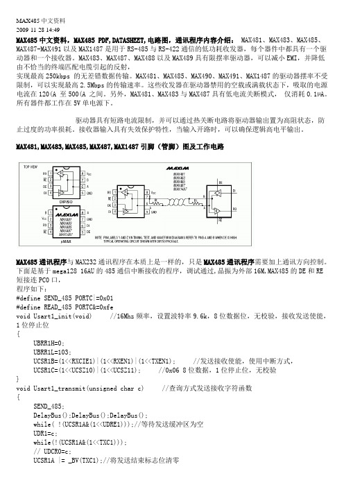
MAX485中文资料2009-11-28 14:49MAX485中文资料,MAX485 PDF,DATASHEET,电路图,通讯程序内容介绍:MAX481、MAX483、MAX485、MAX487-MAX491以及MAX1487是用于RS-485与RS-422通信的低功耗收发器,每个器件中都具有一个驱动器和一个接收器。
MAX483、MAX487、MAX488以及MAX489具有限摆率驱动器,可以减小EMI,并降低由不恰当的终端匹配电缆引起的反射,实现最高250kbps 的无差错数据传输。
MAX481、MAX485、MAX490、MAX491、MAX1487的驱动器摆率不受限制,可以实现最高2.5Mbps的传输速率。
这些收发器在驱动器禁用的空载或满载状态下,吸取的电源电流在120(A 至500(A 之间。
另外,MAX481、MAX483与MAX487具有低电流关断模式,仅消耗0.1µA。
所有器件都工作在5V单电源下。
驱动器具有短路电流限制,并可以通过热关断电路将驱动器输出置为高阻状态,防止过度的功率损耗。
接收器输入具有失效保护特性,当输入开路时,可以确保逻辑高电平输出。
MAX481,MAX483,MAX485,MAX487,MAX1487引脚(管脚)图及工作电路MAX485通讯程序与MAX232通讯程序在本质上是一样的,只是MAX485通讯程序需要加上通讯方向控制。
下面是基于mega128 16AU的485通信中断接收的程序,调试通过,晶振为外部16M,MAX485的DE和RE短接连PC0口,程序如下:#define SEND_485 PORTC|=0x01#define READ_485 PORTC&=0xfevoid Usart1_init(void) //16Mhz频率,设置波特率9.6k,8位数据位,无校验,接收发送使能,1位停止位{UBRR1H=0;UBRR1L=103;UCSR1B=(1<<RXCIE1)|(1<<RXEN1)|(1<<TXEN1); //发送接收使能,使用中断方式,UCSR1C=(1<<UCSZ10)|(1<<UCSZ11); //0x06 8位数据,1位停止位,无校验}void Usart1_transmit(unsigned char c) //查询方式发送接收字符函数{SEND_485;DelayBus();DelayBus();DelayBus();while( !(UCSR1A&(1<<UDRE1)));//等待发送缓冲区为空UDR1=c;while(!(UCSR1A&(1<<TXC1)));// UDCR0=c;UCSR1A |= _BV(TXC1);//将发送结束标志位清零// SET_BIT(UCSR1A,);READ_485;direction++;}SIGNAL(SIG_UART1_RECV)//serial port 1 {if(UCSR1A&(1<<RXC1)){rec1buff=UDR1;rec1_flag=1;。
MAX491EESD+中文资料
Driver Input Voltage (DI).............................-0.5V to (VCC + 0.5V)
Driver Output Voltage (Y, Z; A, B) ..........................-8V to +12.5V
Receiver Input Voltage (A, B).................................-8V to +12.5V
元器件交易网
MAX481E/MAX483E/MAX485E/MAX487E–MAX491E/MAX1487E
±15kV ESD-Protected, Slew-Rate-Limited, Low-Power, RS-485/RS-422 Transceivers
ABSOLUTE MAXIMUM RATINGS
General Description
The MAX481E, MAX483E, MAX485E, MAX487E– MAX491E, and MAX1487E are low-power transceivers for RS-485 and RS-422 communications in harsh environments. Each driver output and receiver input is protected against ±15kV electro-static discharge (ESD) shocks, without latchup. These parts contain one driver and one receiver. The MAX483E, MAX487E, MAX488E, and MAX489E feature reduced slew-rate drivers that minimize EMI and reduce reflections caused by improperly terminated cables, thus allowing error-free data transmission up to 250kbps. The driver slew rates of the MAX481E, MAX485E, MAX490E, MAX491E, and MAX1487E are not limited, allowing them to transmit up to 2.5Mbps.
MEMORY存储芯片MAX488EESA+T中文规格书
±15kV ESD-Protected, Slew-Rate-Limited,Low-Power, RS-485/RS-422 Transceivers__________Function Tables (MAX481E/MAX483E/MAX485E/MAX487E/MAX1487E) Table 1. Transmitting Table 2. Receiving__________Applications Information The MAX481E/MAX483E/MAX485E/MAX487E–MAX491E and MAX1487E are low-power transceivers for RS-485 and RS-422 communications. These “E” versions of the MAX481, MAX483, MAX485, MAX487–MAX491, and MAX1487 provide extra protection against ESD. The rugged MAX481E, MAX483E, MAX485E, MAX497E–MAX491E, and MAX1487E are intended for harsh envi-ronments where high-speed communication is important. These devices eliminate the need for transient suppres-sor diodes and the associated high capacitance loading. The standard (non-“E”) MAX481, MAX483, MAX485, MAX487–MAX491, and MAX1487 are recommended for applications where cost is critical.The MAX481E, MAX485E, MAX490E, MAX491E, and MAX1487E can transmit and receive at data rates up to 2.5Mbps, while the MAX483E, MAX487E, MAX488E, and MAX489E are specified for data rates up to 250kbps. The MAX488E–MAX491E are full-duplex transceivers, while the MAX481E, MAX483E, MAX487E, and MAX1487E are half-duplex. In addition, driver-enable (DE) and receiver-enable (RE) pins are included on the MAX481E, MAX483E, MAX485E, MAX487E, MAX489E, MAX491E, and MAX1487E. When disabled, the driver and receiver outputs are high impedance.±15kV ESD Protection As with all Maxim devices, ESD-protection structures are incorporated on all pins to protect against electro-static discharges encountered during handling and assembly. The driver outputs and receiver inputs have extra protection against static electricity. Maxim’s engi-neers developed state-of-the-art structures to protect these pins against ESD of ±15kV without damage. The ESD structures withstand high ESD in all states: normal operation, shutdown, and powered down. After an ESD event, Maxim’s MAX481E, MAX483E, MAX485E, MAX487E–MAX491E, and MAX1487E keep working without latchup.ESD protection can be tested in various ways; the transmitter outputs and receiver inputs of this product family are characterized for protection to ±15kV using the Human Body Model.Other ESD test methodologies include IEC10004-2 con-tact discharge and IEC1000-4-2 air-gap discharge (for-merly IEC801-2).ESD Test Conditions ESD performance depends on a variety of conditions. Contact Maxim for a reliability report that documents test set-up, test methodology, and test results.Human Body Model F igure 4 shows the Human Body Model, and F igure 5 shows the current waveform it generates when dis-charged into a low impedance. This model consists of a 100pF capacitor charged to the ESD voltage of inter-est, which is then discharged into the test device through a 1.5kΩresistor.IEC1000-4-2 The IEC1000-4-2 standard covers ESD testing and per-formance of finished equipment; it does not specifically refer to integrated circuits (Figure 6).MAX481E/MAX483E/MAX485E/MAX487E–MAX491E/MAX1487E Maxim Integrated9±15kV ESD-Protected, Slew-Rate-Limited, Low-Power, RS-485/RS-422 TransceiversThe major difference between tests done using the Human Body Model and IEC1000-4-2 is higher peak current in IEC1000-4-2, because series resistance is lower in the IEC1000-4-2 model. Hence, the ESD with-stand voltage measured to IEC1000-4-2 is generally lower than that measured using the Human Body Model. Figure 7 shows the current waveform for the 8kV IEC1000-4-2 ESD contact-discharge test.The air-gap test involves approaching the device with a charged probe. The contact-discharge method connects the probe to the device before the probe is energized.Machine Model The Machine Model for ESD tests all pins using a 200pF storage capacitor and zero discharge resis-tance. Its objective is to emulate the stress caused by contact that occurs with handling and assembly during manufacturing. Of course, all pins require this protec-tion during manufacturing—not just inputs and outputs. Therefore,after PC board assembly,the Machine Model is less relevant to I/O ports.MAX487E/MAX1487E:128 Transceivers on the Bus The 48kΩ, 1/4-unit-load receiver input impedance of the MAX487E and MAX1487E allows up to 128 transceivers on a bus, compared to the 1-unit load (12kΩinput impedance) of standard RS-485 drivers (32 transceivers maximum). Any combination of MAX487E/MAX1487E and other RS-485 transceivers with a total of 32 unit loads or less can be put on the bus. The MAX481E, MAX483E, MAX485E, and MAX488E–MAX491E have standard 12kΩreceiver input impedance.MAX483E/MAX487E/MAX488E/MAX489E:Reduced EMI and Reflections The MAX483E and MAX487E–MAX489E are slew-rate limited, minimizing EMI and reducing reflections caused by improperly terminated cables. F igure 16 shows the driver output waveform and its Fourier analy-sis of a 150kHz signal transmitted by a MAX481E, MAX485E, MAX490E, MAX491E, or MAX1487E. High-frequency harmonics with large amplitudes are evident.F igure 17 shows the same information displayed for a MAX483E, MAX487E, MAX488E, or MAX489E transmit-ting under the same conditions. F igure 17’s high-fre-quency harmonics have much lower amplitudes, and the potential for EMI is significantly reduced.Low-Power Shutdown Mode(MAX481E/MAX483E/MAX487E) A low-power shutdown mode is initiated by bringing both RE high and DE low. The devices will not shut down unless both the driver and receiver are disabled. In shutdown, the devices typically draw only 0.5µA of supply current.RE and DE may be driven simultaneously; the parts are guaranteed not to enter shutdown if RE is high and DE is low for less than 50ns. If the inputs are in this state for at least 600ns, the parts are guaranteed to enter shutdown.F or the MAX481E, MAX483E, and MAX487E, the t ZH and t ZL enable times assume the part was not in the low-power shutdown state (the MAX485E, MAX488E–MAX491E, and MAX1487E can not be shut down). The t ZH(SHDN)and t ZL(SHDN)enable times assume the parts were shut down (see Electrical Characteristics).Figure 16. Driver Output Waveform and FFT Plot of MAX485E/MAX490E/MAX491E/MAX1487E Transmitting a 150kHz SignalFigure 17. Driver Output Waveform and FFT Plot ofMAX483E/MAX487E–MAX489E Transmitting a 150kHz SignalMAX481E/MAX483E/MAX485E/ MAX487E–MAX491E/MAX1487E 12。
MAX485EESA+T中文资料

________________________________________________________________ Maxim Integrated Products 1
For pricing, delivery, and ordering information, please contact Maxim/Dallas Direct! at 1-888-629-4642, or visit Maxim’s website at .
Next-Generation Device Features
♦ For Fault-Tolerant Applications: MAX3430: ±80V Fault-Protected, Fail-Safe, 1/4Unit Load, +3.3V, RS-485 Transceiver MAX3080–MAX3089: Fail-Safe, High-Speed (10Mbps), Slew-Rate-Limited, RS-485/RS-422 Transceivers
Ordering Information
PART MAX481ECPA MAX481ECSA MAX481EEPA MAX481EESA MAX483ECPA MAX483ECSA MAX483EEPA MAX483EESA
TEMP RANGE 0°C to +70°C 0°C to +70°C -40°C to +85°C -40°C to +85°C 0°C to +70°C 0°C to +70°C -40°C to +85°C -40°C to +85°C
The MAX487E and MAX1487E feature quarter-unit-load receiver input impedance, allowing up to 128 transceivers on the bus. The MAX488E–MAX491E are designed for full-duplex communications, while the MAX481E, MAX483E, MAX485E, MAX487E, and MAX1487E are designed for half-duplex applications. For applications that are not ESD sensitive see the pinand function-compatible MAX481, MAX483, MAX485, MAX487–MAX491, and MAX1487.
MAX485ECPA中文资料

General DescriptionThe MAX481E, MAX483E, MAX485E, MAX487E–MAX491E, and MAX1487E are low-power transceivers for RS-485 and RS-422 communications in harsh environ-ments. Each driver output and receiver input is protected against ±15kV electro-static discharge (ESD) shocks,without latchup. These parts contain one driver and one receiver. The MAX483E, MAX487E, MAX488E, and MAX489E feature reduced slew-rate drivers that minimize EMI and reduce reflections caused by improperly termi-nated cables, thus allowing error-free data transmission up to 250kbps. The driver slew rates of the MAX481E,MAX485E, MAX490E, MAX491E, and MAX1487E are not limited, allowing them to transmit up to 2.5Mbps.These transceivers draw as little as 120µA supply cur-rent when unloaded or when fully loaded with disabled drivers (see Selector Guide ). Additionally, the MAX481E,MAX483E, and MAX487E have a low-current shutdown mode in which they consume only 0.5µA. All parts oper-ate from a single +5V supply.Drivers are short-circuit current limited, and are protected against excessive power dissipation by thermal shutdown circuitry that places their outputs into a high-impedance state. The receiver input has a fail-safe feature that guar-antees a logic-high output if the input is open circuit.The MAX487E and MAX1487E feature quarter-unit-load receiver input impedance, allowing up to 128 trans-ceivers on the bus. The MAX488E–MAX491E are designed for full-duplex communications, while the MAX481E, MAX483E, MAX485E, MAX487E, and MAX1487E are designed for half-duplex applications.For applications that are not ESD sensitive see the pin-and function-compatible MAX481, MAX483, MAX485,MAX487–MAX491, and MAX1487.ApplicationsLow-Power RS-485 Transceivers Low-Power RS-422 Transceivers Level TranslatorsTransceivers for EMI-Sensitive Applications Industrial-Control Local Area NetworksNext-Generation Device Features♦For Fault-Tolerant Applications:MAX3430: ±80V Fault-Protected, Fail-Safe, 1/4-Unit Load, +3.3V, RS-485 TransceiverMAX3080–MAX3089: Fail-Safe, High-Speed (10Mbps), Slew-Rate-Limited, RS-485/RS-422Transceivers ♦For Space-Constrained Applications:MAX3460–MAX3464: +5V, Fail-Safe, 20Mbps,Profibus, RS-485/RS-422 TransceiversMAX3362: +3.3V, High-Speed, RS-485/RS-422Transceiver in a SOT23 PackageMAX3280E–MAX3284E: ±15kV ESD-Protected,52Mbps, +3V to +5.5V, SOT23, RS-485/RS-422True Fail-Safe ReceiversMAX3030E–MAX3033E: ±15kV ESD-Protected,+3.3V, Quad RS-422 Transmitters ♦For Multiple Transceiver Applications:MAX3293/MAX3294/MAX3295: 20Mbps, +3.3V,SOT23, RS-485/RS-422 Transmitters ♦For Fail-Safe Applications:MAX3440E–MAX3444E: ±15kV ESD-Protected,±60V Fault-Protected, 10Mbps, Fail-Safe RS-485/J1708 Transceivers ♦For Low-Voltage Applications:MAX3483E/MAX3485E/MAX3486E/MAX3488E/MAX3490E/MAX3491E: +3.3V Powered, ±15kV ESD-Protected, 12Mbps, Slew-Rate-Limited, True RS-485/RS-422 TransceiversMAX481E/MAX483E/MAX485E/MAX487E–MAX491E/MAX1487E±15kV ESD-Protected, Slew-Rate-Limited, Low-Power, RS-485/RS-422 Transceivers________________________________________________________________Maxim Integrated Products 1Ordering Information19-0410; Rev 4; 10/03For pricing, delivery, and ordering information,please contact Maxim/Dallas Direct!at 1-888-629-4642, or visit Maxim’s website at .Ordering Information continued at end of data sheet.Selector Guide appears at end of data sheet .M A X 481E /M A X 483E /M A X 485E /M A X 487E –M A X 491E /M A X 1487E±15kV ESD-Protected, Slew-Rate-Limited,Low-Power, RS-485/RS-422 Transceivers2_______________________________________________________________________________________Supply Voltage (V CC ) (12V)Control Input Voltage (–R —E –, DE)...................-0.5V to (V CC + 0.5V)Driver Input Voltage (DI).............................-0.5V to (V CC + 0.5V)Driver Output Voltage (Y, Z; A, B)..........................-8V to +12.5V Receiver Input Voltage (A, B).................................-8V to +12.5V Receiver Output Voltage (RO)....................-0.5V to (V CC + 0.5V)Continuous Power Dissipation (T A = +70°C)8-Pin Plastic DIP (derate 9.09mW/°C above +70°C)....727mW14-Pin Plastic DIP (derate 10.00mW/°C above +70°C)..800mW 8-Pin SO (derate 5.88mW/°C above +70°C).................471mW 14-Pin SO (derate 8.33mW/°C above +70°C)...............667mW Operating Temperature RangesMAX4_ _C_ _/MAX1487EC_ A.............................0°C to +70°C MAX4__E_ _/MAX1487EE_ A...........................-40°C to +85°C Storage Temperature Range.............................-65°C to +160°C Lead Temperature (soldering, 10sec).............................+300°CDC ELECTRICAL CHARACTERISTICS(V CC = 5V ±5%, T A = T MIN to T MAX , unless otherwise noted.) (Notes 1, 2)Stresses beyond those listed under “Absolute Maximum Ratings” may cause permanent damage to the device. These are stress ratings only, and functional operation of the device at these or any other conditions beyond those indicated in the operational sections of the specifications is not implied. Exposure to absolute maximum rating conditions for extended periods may affect device reliability.ABSOLUTE MAXIMUM RATINGSPARAMETERSYMBOL MINTYPMAX UNITS Driver Common-Mode Output VoltageV OC 3V Change in Magnitude of Driver Differential Output Voltage for Complementary Output States ∆V OD 0.2V Change in Magnitude of Driver Common-Mode Output Voltage for Complementary Output States ∆V OD 0.2V Input High Voltage V IH 2.0V Input Low Voltage V IL 0.8V Input CurrentI IN1±2µADifferential Driver Output (no load)V OD15V 2V Differential Driver Output (with load)V OD2 1.551.0-0.8mA0.25mA -0.2Receiver Differential Threshold Voltage-0.20.2V Receiver Input Hysteresis ∆V TH 70mV Receiver Output High Voltage V OH 3.5Receiver Output Low Voltage V OL 0.4V Three-State (high impedance)Output Current at ReceiverI OZR±1µA 12k ΩCONDITIONSDE = 0V;V CC = 0V or 5.25V,all devices except MAX487E/MAX1487E R = 27Ωor 50Ω, Figure 8R = 27Ωor 50Ω, Figure 8R = 27Ωor 50Ω, Figure 8DE, DI, –R —E–MAX487E/MAX1487E,DE = 0V, V CC = 0V or 5.25VDE, DI, –R —E–DE, DI, –R —E–-7V ≤V CM ≤12V V CM = 0VI O = -4mA, V ID = 200mV I O = 4mA, V ID = -200mV R = 50Ω(RS-422)0.4V ≤V O ≤2.4VR = 27Ω(RS-485), Figure 8-7V ≤V CM ≤12V, all devices except MAX487E/MAX1487EReceiver Input Resistance R IN-7V ≤V CM ≤12V, MAX487E/MAX1487E48k ΩV TH I IN2Input Current (A, B)V IN = 12V V IN = -7V V IN = 12V V IN = -7VVMAX481E/MAX483E/MAX485E/MAX487E–MAX491E/MAX1487E±15kV ESD-Protected, Slew-Rate-Limited,Low-Power, RS-485/RS-422 TransceiversSWITCHING CHARACTERISTICS—MAX481E/MAX485E, MAX490E/MAX491E, MAX1487EDC ELECTRICAL CHARACTERISTICS (continued)(V CC = 5V ±5%, T A = T MIN to T MAX , unless otherwise noted.) (Notes 1, 2)M A X 481E /M A X 483E /M A X 485E /M A X 487E –M A X 491E /M A X 1487E±15kV ESD-Protected, Slew-Rate-Limited,Low-Power, RS-485/RS-422 Transceivers4_______________________________________________________________________________________SWITCHING CHARACTERISTICS—MAX483E, MAX487E/MAX488E/MAX489E(V CC = 5V ±5%, T A = T MIN to T MAX , unless otherwise noted.) (Notes 1, 2)SWITCHING CHARACTERISTICS—MAX481E/MAX485E, MAX490E/MAX491E, MAX1487E(continued)(V CC = 5V ±5%, T A = T MIN to T MAX , unless otherwise noted.) (Notes 1, 2)2251000Figures 11 and 13, C L = 100pF, S2 closed Figures 11 and 13, C L = 100pF, S1 closed Figures 9 and 15, C L = 15pF, S2 closed,A - B = 2VCONDITIONSns 45100t ZH(SHDN)Driver Enable from Shutdown toOutput High (MAX481E)nsFigures 9 and 15, C L = 15pF, S1 closed,B - A = 2Vt ZL(SHDN)Receiver Enable from Shutdownto Output Low (MAX481E)ns 45100t ZL(SHDN)Driver Enable from Shutdown toOutput Low (MAX481E)ns 2251000t ZH(SHDN)Receiver Enable from Shutdownto Output High (MAX481E)UNITS MINTYP MAX SYMBOLPARAMETERt PLH t SKEW Figures 10 and 12, R DIFF = 54Ω,C L1= C L2= 100pFt PHL Figures 10 and 12, R DIFF = 54Ω,C L1= C L2= 100pFDriver Input to Output Driver Output Skew to Output ns 20800ns ns 2000MAX483E/MAX487E, Figures 11 and 13,C L = 100pF, S2 closedt ZH(SHDN)Driver Enable from Shutdown to Output High2502000ns2500MAX483E/MAX487E, Figures 9 and 15,C L = 15pF, S1 closedt ZL(SHDN)Receiver Enable from Shutdown to Output Lowns 2500MAX483E/MAX487E, Figures 9 and 15,C L = 15pF, S2 closedt ZH(SHDN)Receiver Enable from Shutdown to Output Highns 2000MAX483E/MAX487E, Figures 11 and 13,C L = 100pF, S1 closedt ZL(SHDN)Driver Enable from Shutdown to Output Lowns 50200600MAX483E/MAX487E (Note 5)t SHDN Time to Shutdownt PHL t PLH , t PHL < 50% of data period Figures 9 and 15, C RL = 15pF, S2 closed Figures 9 and 15, C RL = 15pF, S1 closed Figures 9 and 15, C RL = 15pF, S2 closed Figures 9 and 15, C RL = 15pF, S1 closed Figures 11 and 13, C L = 15pF, S2 closed Figures 10 and 14, R DIFF = 54Ω,C L1= C L2= 100pFFigures 11 and 13, C L = 15pF, S1 closed Figures 11 and 13, C L = 100pF, S1 closed Figures 11 and 13, C L = 100pF, S2 closed CONDITIONSkbps 250f MAX 2508002000Maximum Data Rate ns 2550t HZ Receiver Disable Time from High ns 25080020002550t LZ Receiver Disable Time from Low ns 2550t ZH Receiver Enable to Output High ns 2550t ZL Receiver Enable to Output Low ns ns 1003003000t HZ t SKD Driver Disable Time from High I t PLH - t PHL I DifferentialReceiver SkewFigures 10 and 14, R DIFF = 54Ω,C L1= C L2= 100pFns 3003000t LZ Driver Disable Time from Low ns 2502000t ZL Driver Enable to Output Low ns Figures 10 and 12, R DIFF = 54Ω,C L1= C L2= 100pFns 2502000t R , t F 2502000Driver Rise or Fall Time ns t PLH Receiver Input to Output2502000t ZH Driver Enable to Output High UNITS MIN TYP MAX SYMBOL PARAMETERMAX481E/MAX483E/MAX485E/MAX487E–MAX491E/MAX1487E±15kV ESD-Protected, Slew-Rate-Limited,Low-Power, RS-485/RS-422 Transceivers_______________________________________________________________________________________505101520253035404550OUTPUT CURRENT vs.RECEIVER OUTPUT LOW VOLTAGEM A X 481E -01OUTPUT LOW VOLTAGE (V)O U T P U T C U R R E N T (m A )1.52.02.51.00.50.10.20.30.40.50.60.70.80.9-60-2060RECEIVER OUTPUT LOW VOLTAGEvs. TEMPERATURETEMPERATURE (°C)O U T P U T L O W V O L T A G E (V )20100-4040800-5-10-15-20-251.53.0OUTPUT CURRENT vs.RECEIVER OUTPUT HIGH VOLTAGEM A X 481E -02OUTPUT HIGH VOLTAGE (V)O U T P U T C U R R E N T (m A )5.04.54.02.02.53.53.03.23.43.63.84.04.24.44.64.8-60-2060RECEIVER OUTPUT HIGH VOLTAGEvs. TEMPERATURETEMPERATURE (°C)O U T P U T H I G H V O L T A G E (V )20100-4040800102030405060708090DRIVER OUTPUT CURRENT vs. DIFFERENTIAL OUTPUT VOLTAGEM A X 481E -05DIFFERENTIAL OUTPUT VOLTAGE (V)O U T P U T C U R R E N T (m A )1.52.0 2.53.0 3.54.0 4.51.00.50__________________________________________Typical Operating Characteristics(V CC = 5V, T A = +25°C, unless otherwise noted.)NOTES FOR ELECTRICAL/SWITCHING CHARACTERISTICSNote 1:All currents into device pins are positive; all currents out of device pins are negative. All voltages are referenced to deviceground unless otherwise specified.Note 2:All typical specifications are given for V CC = 5V and T A = +25°C.Note 3:Supply current specification is valid for loaded transmitters when DE = 0V.Note 4:Applies to peak current. See Typical Operating Characteristics.Note 5:The MAX481E/MAX483E/MAX487E are put into shutdown by bringing –R —E –high and DE low. If the inputs are in this state forless than 50ns, the parts are guaranteed not to enter shutdown. If the inputs are in this state for at least 600ns, the parts are guaranteed to have entered shutdown. See Low-Power Shutdown Mode section.M A X 481E /M A X 483E /M A X 485E /M A X 487E –M A X 491E /M A X 1487E±15kV ESD-Protected, Slew-Rate-Limited,Low-Power, RS-485/RS-422 Transceivers6___________________________________________________________________________________________________________________Typical Operating Characteristics (continued)(V CC = 5V, T A = +25°C, unless otherwise noted.)1.52.32.22.12.01.91.81.71.6-60-2060DRIVER DIFFERENTIAL OUTPUT VOLTAGE vs. TEMPERATURETEMPERATURE (°C)D I F FE R E N T I A L O U T P U T V O L T A G E (V )20100-404080020406080100120140OUTPUT CURRENT vs. DRIVER OUTPUT LOW VOLTAGEM A X 481E -07OUTPUT LOW VOLTAGE (V)O U T P U T C U R R E N T (m A )246810120-10-20-30-40-50-60-70-80-90-100-8-2OUTPUT CURRENT vs. DRIVER OUTPUT HIGH VOLTAGEM A X 481E -08OUTPUT HIGH VOLTAGE (V)O U T P U T C U R R E N T (m A )642-6-400100200300400500600-60-2060MAX481E/MAX485E/MAX490E/MAX491E SUPPLY CURRENT vs. TEMPERATURETEMPERATURE (°C)S U P P L Y C U R R E N T (µA )20100-4040800100200300400500600-60-2060MAX483E/MAX487E–MAX489E SUPPLY CURRENT vs. TEMPERATURETEMPERATURE (°C)S U P P L Y C U R R E N T (µA )20100-404080100200300400500600-60-2060MAX1487ESUPPLY CURRENT vs. TEMPERATURETEMPERATURE (°C)S U P P L Y C U R R E N T (µA )20100-404080±15kV ESD-Protected, Slew-Rate-Limited, Low-Power, RS-485/RS-422 Transceivers_______________________________________________________________________________________7MAX481E/MAX483E/MAX485E/MAX487E–MAX491E/MAX1487E______________________________________________________________Pin DescriptionM A X 481E /M A X 483E /M A X 485E /M A X 487E –M A X 491E /M A X 1487E±15kV ESD-Protected, Slew-Rate-Limited,Low-Power, RS-485/RS-422 Transceivers8_________________________________________________________________________________________________Function Tables (MAX481E/MAX483E/MAX485E/MAX487E/MAX1487E) Table 1. Transmitting__________Applications Information The MAX481E/MAX483E/MAX485E/MAX487E–MAX491E and MAX1487E are low-power transceivers for RS-485 and RS-422 communications. These “E” versions of the MAX481, MAX483, MAX485, MAX487–MAX491, and MAX1487 provide extra protection against ESD. The rugged MAX481E, MAX483E, MAX485E, MAX497E–MAX491E, and MAX1487E are intended for harsh envi-ronments where high-speed communication is important. These devices eliminate the need for transient suppres-sor diodes and the associated high capacitance loading. The standard (non-“E”) MAX481, MAX483, MAX485, MAX487–MAX491, and MAX1487 are recommended for applications where cost is critical.The MAX481E, MAX485E, MAX490E, MAX491E, and MAX1487E can transmit and receive at data rates up to 2.5Mbps, while the MAX483E, MAX487E, MAX488E, and MAX489E are specified for data rates up to 250kbps. The MAX488E–MAX491E are full-duplex transceivers, while the MAX481E, MAX483E, MAX487E, and MAX1487E are half-duplex. In addition, driver-enable (DE) and receiver-enable (RE) pins are included on the MAX481E, MAX483E, MAX485E, MAX487E, MAX489E, MAX491E, and MAX1487E. When disabled, the driver and receiver outputs are high impedance.±15kV ESD Protection As with all Maxim devices, ESD-protection structures are incorporated on all pins to protect against electro-static discharges encountered during handling and assembly. The driver outputs and receiver inputs have extra protection against static electricity. Maxim’s engi-neers developed state-of-the-art structures to protect these pins against ESD of ±15kV without damage. The ESD structures withstand high ESD in all states: normal operation, shutdown, and powered down. After an ESD event, Maxim’s MAX481E, MAX483E, MAX485E, MAX487E–MAX491E, and MAX1487E keep working without latchup.ESD protection can be tested in various ways; the transmitter outputs and receiver inputs of this product family are characterized for protection to ±15kV using the Human Body Model.Other ESD test methodologies include IEC10004-2 con-tact discharge and IEC1000-4-2 air-gap discharge (for-merly IEC801-2).ESD Test Conditions ESD performance depends on a variety of conditions. Contact Maxim for a reliability report that documents test set-up, test methodology, and test results.Human Body Model Figure 4 shows the Human Body Model, and Figure 5 shows the current waveform it generates when dis-charged into a low impedance. This model consists of a 100pF capacitor charged to the ESD voltage of inter-est, which is then discharged into the test device through a 1.5kΩresistor.IEC1000-4-2 The IEC1000-4-2 standard covers ESD testing and per-formance of finished equipment; it does not specifically refer to integrated circuits (Figure 6).MAX481E/MAX483E/MAX485E/MAX487E–MAX491E/MAX1487E±15kV ESD-Protected, Slew-Rate-Limited,Low-Power, RS-485/RS-422 Transceivers_______________________________________________________________________________________9M A X 481E /M A X 483E /M A X 485E /M A X 487E –M A X 491E /M A X 1487E±15kV ESD-Protected, Slew-Rate-Limited,Low-Power, RS-485/RS-422 Transceivers10______________________________________________________________________________________Figure 8. Driver DC Test LoadFigure 9. Receiver Timing Test LoadMAX481E/MAX483E/MAX485E/MAX487E–MAX491E/MAX1487E±15kV ESD-Protected, Slew-Rate-Limited,Low-Power, RS-485/RS-422 Transceivers______________________________________________________________________________________11Figure 10. Driver/Receiver Timing Test Circuit Figure 11. Driver Timing Test LoadFigure 12. Driver Propagation DelaysFigure 13. Driver Enable and Disable Times (except MAX488E and MAX490E)Figure 14. Receiver Propagation DelaysFigure 15. Receiver Enable and Disable Times (except MAX488E and MAX490E)M A X 481E /M A X 483E /M A X 485E /M A X 487E –M A X 491E /M A X 1487E±15kV ESD-Protected, Slew-Rate-Limited,Low-Power, RS-485/RS-422 Transceivers12______________________________________________________________________________________The major difference between tests done using the Human Body Model and IEC1000-4-2 is higher peak current in IEC1000-4-2, because series resistance is lower in the IEC1000-4-2 model. Hence, the ESD with-stand voltage measured to IEC1000-4-2 is generally lower than that measured using the Human Body Model. Figure 7 shows the current waveform for the 8kV IEC1000-4-2 ESD contact-discharge test.The air-gap test involves approaching the device with a charged probe. The contact-discharge method connects the probe to the device before the probe is energized.Machine ModelThe Machine Model for ESD tests all pins using a 200pF storage capacitor and zero discharge resis-tance. Its objective is to emulate the stress caused by contact that occurs with handling and assembly during manufacturing. Of course, all pins require this protec-tion during manufacturing—not just inputs and outputs.Therefore,after PC board assembly,the Machine Model is less relevant to I/O ports.MAX487E/MAX1487E:128 Transceivers on the BusThe 48k Ω, 1/4-unit-load receiver input impedance of the MAX487E and MAX1487E allows up to 128 transceivers on a bus, compared to the 1-unit load (12k Ωinput impedance) of standard RS-485 drivers (32 transceivers maximum). Any combination of MAX487E/MAX1487E and other RS-485 transceivers with a total of 32 unit loads or less can be put on the bus. The MAX481E,MAX483E, MAX485E, and MAX488E–MAX491E have standard 12k Ωreceiver input impedance.MAX483E/MAX487E/MAX488E/MAX489E:Reduced EMI and Reflections The MAX483E and MAX487E–MAX489E are slew-rate limited, minimizing EMI and reducing reflections caused by improperly terminated cables. Figure 16shows the driver output waveform and its Fourier analy-sis of a 150kHz signal transmitted by a MAX481E,MAX485E, MAX490E, MAX491E, or MAX1487E. High-frequency harmonics with large amplitudes are evident.Figure 17 shows the same information displayed for a MAX483E, MAX487E, MAX488E, or MAX489E transmit-ting under the same conditions. Figure 17’s high-fre-quency harmonics have much lower amplitudes, and the potential for EMI is significantly reduced.Low-Power Shutdown Mode (MAX481E/MAX483E/MAX487E)A low-power shutdown mode is initiated by bringing both RE high and DE low. The devices will not shut down unless both the driver and receiver are disabled.In shutdown, the devices typically draw only 0.5µA of supply current.RE and DE may be driven simultaneously; the parts are guaranteed not to enter shutdown if RE is high and DE is low for less than 50ns. If the inputs are in this state for at least 600ns, the parts are guaranteed to enter shutdown.For the MAX481E, MAX483E, and MAX487E, the t ZH and t ZL enable times assume the part was not in the low-power shutdown state (the MAX485E, MAX488E–MAX491E, and MAX1487E can not be shut down). The t ZH(SHDN)and t ZL(SHDN)enable times assume the parts were shut down (see Electrical Characteristics ).500kHz/div0Hz5MHz 10dB/div Figure 16. Driver Output Waveform and FFT Plot ofMAX485E/MAX490E/MAX491E/MAX1487E Transmitting a 150kHz Signal500kHz/div0Hz5MHz10dB/divFigure 17. Driver Output Waveform and FFT Plot ofMAX483E/MAX487E–MAX489E Transmitting a 150kHz SignalIt takes the drivers and receivers longer to become enabled from the low-power shutdown state (t ZH(SHDN), t ZL(SHDN)) than from the operating mode (t ZH, t ZL). (The parts are in operating mode if the RE, DE inputs equal a logical 0,1 or 1,1 or 0, 0.)Driver Output Protection Excessive output current and power dissipation caused by faults or by bus contention are prevented by two mechanisms. A foldback current limit on the output stage provides immediate protection against short circuits over the whole common-mode voltage range (see Typical Operating Characteristics). In addition, a thermal shut-down circuit forces the driver outputs into a high-imped-ance state if the die temperature rises excessively.Propagation Delay Many digital encoding schemes depend on the differ-ence between the driver and receiver propagation delay times. Typical propagation delays are shown in Figures 19–22 using Figure 18’s test circuit.The difference in receiver delay times, t PLH- t PHL, is typically under 13ns for the MAX481E, MAX485E, MAX490E, MAX491E, and MAX1487E, and is typically less than 100ns for the MAX483E and MAX487E–MAX489E.The driver skew times are typically 5ns (10ns max) for the MAX481E, MAX485E, MAX490E, MAX491E, and MAX1487E, and are typically 100ns (800ns max) for the MAX483E and MAX487E–MAX489E.Typical Applications The MAX481E, MAX483E, MAX485E, MAX487E–MAX491E, and MAX1487E transceivers are designed for bidirectional data communications on multipoint bus transmission lines. Figures 25 and 26 show typical net-work application circuits. These parts can also be used as line repeaters, with cable lengths longer than 4000 feet. To minimize reflections, the line should be terminated at both ends in its characteristic impedance, and stub lengths off the main line should be kept as short as possi-ble. The slew-rate-limited MAX483E and MAX487E–MAX489E are more tolerant of imperfect termination. Bypass the V CC pin with 0.1µF.Isolated RS-485 For isolated RS-485 applications, see the MAX253 and MAX1480 data sheets.Line Length vs. Data Rate The RS-485/RS-422 standard covers line lengths up to 4000 feet. Figures 23 and 24 show the system differen-tial voltage for the parts driving 4000 feet of 26AWG twisted-pair wire at 110kHz into 100Ωloads.Figure 18. Receiver Propagation Delay Test CircuitMAX481E/MAX483E/MAX485E/MAX487E–MAX491E/MAX1487E±15kV ESD-Protected, Slew-Rate-Limited,Low-Power, RS-485/RS-422 Transceivers ______________________________________________________________________________________13M A X 481E /M A X 483E /M A X 485E /M A X 487E –M A X 491E /M A X 1487E±15kV ESD-Protected, Slew-Rate-Limited,Low-Power, RS-485/RS-422 Transceivers14______________________________________________________________________________________25ns/div 5V/divRO B A500mV/div Figure 19. MAX481E/MAX485E/MAX490E/MAX1487E Receiver t PHL25ns/div5V/div ROBA500mV/divFigure 20. MAX481E/MAX485E/MAX490E/MAX491E/MAX1487E Receiver t PLH200ns/div 5V/divRO B A500mV/div Figure 21. MAX483E/MAX487E–MAX489E Receiver t PHL200ns/div5V/div ROBA500mV/divFigure 22. MAX483E/MAX487E–MAX489E Receiver t PLH2µs/div DO 0V0V5V5V -1V 0DIV A - V BFigure 23. MAX481E/MAX485E/MAX490E/MAX491E/MAX1487E System Differential Voltage at 110kHz Driving 4000ft of Cable 2µs/divDO0V0V 5V 5V -1V1V0DIV B - V AFigure 24. MAX483E/MAX1487E–MAX489E System Differential Voltage at 110kHz Driving 4000ft of CableMAX481E/MAX483E/MAX485E/MAX487E–MAX491E/MAX1487E±15kV ESD-Protected, Slew-Rate-Limited,Low-Power, RS-485/RS-422 Transceivers______________________________________________________________________________________15Figure 26. MAX488E–MAX491E Full-Duplex RS-485 NetworkFigure 25. MAX481E/MAX483E/MAX485E/MAX487E/MAX1487E Typical Half-Duplex RS-485 NetworkM A X 481E /M A X 483E /M A X 485E /M A X 487E –M A X 491E /M A X 1487E±15kV ESD-Protected, Slew-Rate-Limited, Low-Power, RS-485/RS-422 Transceivers Maxim cannot assume responsibility for use of any circuitry other than circuitry entirely embodied in a Maxim product. No circuit patent licenses are implied. Maxim reserves the right to change the circuitry and specifications without notice at any time.16____________________Maxim Integrated Products, 120 San Gabriel Drive, Sunnyvale, CA 94086 408-737-7600©2003 Maxim Integrated ProductsPrinted USAis a registered trademark of Maxim Integrated Products.Package InformationFor the latest package outline information, go to /packages .Ordering Information (continued)Selector GuideChip InformationTRANSISTOR COUNT: 295。
MAX488ESA-T中文资料

For pricing, delivery, and ordering information,please contact Maxim/Dallas Direct!at 1-888-629-4642, or visit Maxim’s website at .General DescriptionThe MAX481, MAX483, MAX485, MAX487–MAX491, and MAX1487 are low-power transceivers for RS-485 and RS-422 communication. Each part contains one driver and one receiver. The MAX483, MAX487, MAX488, and MAX489feature reduced slew-rate drivers that minimize EMI and reduce reflections caused by improperly terminated cables,thus allowing error-free data transmission up to 250kbps.The driver slew rates of the MAX481, MAX485, MAX490,MAX491, and MAX1487 are not limited, allowing them to transmit up to 2.5Mbps.These transceivers draw between 120µA and 500µA of supply current when unloaded or fully loaded with disabled drivers. Additionally, the MAX481, MAX483, and MAX487have a low-current shutdown mode in which they consume only 0.1µA. All parts operate from a single 5V supply.Drivers are short-circuit current limited and are protected against excessive power dissipation by thermal shutdown circuitry that places the driver outputs into a high-imped-ance state. The receiver input has a fail-safe feature that guarantees a logic-high output if the input is open circuit.The MAX487 and MAX1487 feature quarter-unit-load receiver input impedance, allowing up to 128 MAX487/MAX1487 transceivers on the bus. Full-duplex communi-cations are obtained using the MAX488–MAX491, while the MAX481, MAX483, MAX485, MAX487, and MAX1487are designed for half-duplex applications.________________________ApplicationsLow-Power RS-485 Transceivers Low-Power RS-422 Transceivers Level TranslatorsTransceivers for EMI-Sensitive Applications Industrial-Control Local Area Networks__Next Generation Device Features♦For Fault-Tolerant ApplicationsMAX3430: ±80V Fault-Protected, Fail-Safe, 1/4Unit Load, +3.3V, RS-485 TransceiverMAX3440E–MAX3444E: ±15kV ESD-Protected,±60V Fault-Protected, 10Mbps, Fail-Safe, RS-485/J1708 Transceivers♦For Space-Constrained ApplicationsMAX3460–MAX3464: +5V, Fail-Safe, 20Mbps,Profibus RS-485/RS-422 TransceiversMAX3362: +3.3V, High-Speed, RS-485/RS-422Transceiver in a SOT23 PackageMAX3280E–MAX3284E: ±15kV ESD-Protected,52Mbps, +3V to +5.5V, SOT23, RS-485/RS-422,True Fail-Safe ReceiversMAX3293/MAX3294/MAX3295: 20Mbps, +3.3V,SOT23, RS-855/RS-422 Transmitters ♦For Multiple Transceiver ApplicationsMAX3030E–MAX3033E: ±15kV ESD-Protected,+3.3V, Quad RS-422 Transmitters ♦For Fail-Safe ApplicationsMAX3080–MAX3089: Fail-Safe, High-Speed (10Mbps), Slew-Rate-Limited RS-485/RS-422Transceivers♦For Low-Voltage ApplicationsMAX3483E/MAX3485E/MAX3486E/MAX3488E/MAX3490E/MAX3491E: +3.3V Powered, ±15kV ESD-Protected, 12Mbps, Slew-Rate-Limited,True RS-485/RS-422 TransceiversMAX481/MAX483/MAX485/MAX487–MAX491/MAX1487Low-Power, Slew-Rate-Limited RS-485/RS-422 Transceivers______________________________________________________________Selection Table19-0122; Rev 8; 10/03Ordering Information appears at end of data sheet.M A X 481/M A X 483/M A X 485/M A X 487–M A X 491/M A X 1487Low-Power, Slew-Rate-Limited RS-485/RS-422 Transceivers 2_______________________________________________________________________________________ABSOLUTE MAXIMUM RATINGSSupply Voltage (V CC ).............................................................12V Control Input Voltage (RE , DE)...................-0.5V to (V CC + 0.5V)Driver Input Voltage (DI).............................-0.5V to (V CC + 0.5V)Driver Output Voltage (A, B)...................................-8V to +12.5V Receiver Input Voltage (A, B).................................-8V to +12.5V Receiver Output Voltage (RO).....................-0.5V to (V CC +0.5V)Continuous Power Dissipation (T A = +70°C)8-Pin Plastic DIP (derate 9.09mW/°C above +70°C)....727mW 14-Pin Plastic DIP (derate 10.00mW/°C above +70°C)..800mW 8-Pin SO (derate 5.88mW/°C above +70°C).................471mW14-Pin SO (derate 8.33mW/°C above +70°C)...............667mW 8-Pin µMAX (derate 4.1mW/°C above +70°C)..............830mW 8-Pin CERDIP (derate 8.00mW/°C above +70°C).........640mW 14-Pin CERDIP (derate 9.09mW/°C above +70°C).......727mW Operating Temperature RangesMAX4_ _C_ _/MAX1487C_ A...............................0°C to +70°C MAX4__E_ _/MAX1487E_ A.............................-40°C to +85°C MAX4__MJ_/MAX1487MJA...........................-55°C to +125°C Storage Temperature Range.............................-65°C to +160°C Lead Temperature (soldering, 10sec).............................+300°CDC ELECTRICAL CHARACTERISTICS(V CC = 5V ±5%, T A = T MIN to T MAX , unless otherwise noted.) (Notes 1, 2)Stresses beyond those listed under “Absolute Maximum Ratings” may cause permanent damage to the device. These are stress ratings only, and functional operation of the device at these or any other conditions beyond those indicated in the operational sections of the specifications is not implied. Exposure to absolute maximum rating conditions for extended periods may affect device reliability.V V IN = -7VV IN = 12V V IN = -7V V IN = 12V Input Current (A, B)I IN2V TH k Ω48-7V ≤V CM ≤12V, MAX487/MAX1487R INReceiver Input Resistance -7V ≤V CM ≤12V, all devices except MAX487/MAX1487R = 27Ω(RS-485), Figure 40.4V ≤V O ≤2.4VR = 50Ω(RS-422)I O = 4mA, V ID = -200mV I O = -4mA, V ID = 200mV V CM = 0V-7V ≤V CM ≤12V DE, DI, RE DE, DI, RE MAX487/MAX1487,DE = 0V, V CC = 0V or 5.25VDE, DI, RE R = 27Ωor 50Ω, Figure 4R = 27Ωor 50Ω, Figure 4R = 27Ωor 50Ω, Figure 4DE = 0V;V CC = 0V or 5.25V,all devices except MAX487/MAX1487CONDITIONSk Ω12µA ±1I OZRThree-State (high impedance)Output Current at ReceiverV 0.4V OL Receiver Output Low Voltage 3.5V OH Receiver Output High Voltage mV 70∆V TH Receiver Input Hysteresis V -0.20.2Receiver Differential Threshold Voltage-0.2mA 0.25mA-0.81.01.55V OD2Differential Driver Output (with load)V 2V 5V OD1Differential Driver Output (no load)µA±2I IN1Input CurrentV 0.8V IL Input Low Voltage V 2.0V IH Input High Voltage V 0.2∆V OD Change in Magnitude of Driver Common-Mode Output Voltage for Complementary Output States V 0.2∆V OD Change in Magnitude of Driver Differential Output Voltage for Complementary Output States V 3V OC Driver Common-Mode Output VoltageUNITS MINTYPMAX SYMBOL PARAMETERMAX481/MAX483/MAX485/MAX487–MAX491/MAX1487Low-Power, Slew-Rate-Limited RS-485/RS-422 Transceivers_______________________________________________________________________________________3SWITCHING CHARACTERISTICS—MAX481/MAX485, MAX490/MAX491, MAX1487(V CC = 5V ±5%, T A = T MIN to T MAX , unless otherwise noted.) (Notes 1, 2)DC ELECTRICAL CHARACTERISTICS (continued)(V CC = 5V ±5%, T A = T MIN to T MAX , unless otherwise noted.) (Notes 1, 2)ns 103060t PHLDriver Rise or Fall Time Figures 6 and 8, R DIFF = 54Ω, C L1= C L2= 100pF ns MAX490M, MAX491M MAX490C/E, MAX491C/E2090150MAX481, MAX485, MAX1487MAX490M, MAX491MMAX490C/E, MAX491C/E MAX481, MAX485, MAX1487Figures 6 and 8, R DIFF = 54Ω,C L1= C L2= 100pF MAX481 (Note 5)Figures 5 and 11, C RL = 15pF, S2 closedFigures 5 and 11, C RL = 15pF, S1 closed Figures 5 and 11, C RL = 15pF, S2 closed Figures 5 and 11, C RL = 15pF, S1 closed Figures 6 and 10, R DIFF = 54Ω,C L1= C L2= 100pFFigures 6 and 8,R DIFF = 54Ω,C L1= C L2= 100pF Figures 6 and 10,R DIFF = 54Ω,C L1= C L2= 100pF CONDITIONS ns 510t SKEW ns50200600t SHDNTime to ShutdownMbps 2.5f MAX Maximum Data Rate ns 2050t HZ Receiver Disable Time from High ns 103060t PLH 2050t LZ Receiver Disable Time from Low ns 2050t ZH Driver Input to Output Receiver Enable to Output High ns 2050t ZL Receiver Enable to Output Low 2090200ns ns 134070t HZ t SKD Driver Disable Time from High |t PLH - t PHL |DifferentialReceiver Skewns 4070t LZ Driver Disable Time from Low ns 4070t ZL Driver Enable to Output Low 31540ns51525ns 31540t R , t F 2090200Driver Output Skew to Output t PLH , t PHL Receiver Input to Output4070t ZH Driver Enable to Output High UNITS MIN TYP MAX SYMBOL PARAMETERFigures 7 and 9, C L = 100pF, S2 closed Figures 7 and 9, C L = 100pF, S1 closed Figures 7 and 9, C L = 15pF, S1 closed Figures 7 and 9, C L = 15pF, S2 closedM A X 481/M A X 483/M A X 485/M A X 487–M A X 491/M A X 1487Low-Power, Slew-Rate-Limited RS-485/RS-422 Transceivers 4_______________________________________________________________________________________SWITCHING CHARACTERISTICS—MAX483, MAX487/MAX488/MAX489(V CC = 5V ±5%, T A = T MIN to T MAX , unless otherwise noted.) (Notes 1, 2)SWITCHING CHARACTERISTICS—MAX481/MAX485, MAX490/MAX491, MAX1487 (continued)(V CC = 5V ±5%, T A = T MIN to T MAX , unless otherwise noted.) (Notes 1, 2)3001000Figures 7 and 9, C L = 100pF, S2 closed Figures 7 and 9, C L = 100pF, S1 closed Figures 5 and 11, C L = 15pF, S2 closed,A - B = 2VCONDITIONSns 40100t ZH(SHDN)Driver Enable from Shutdown toOutput High (MAX481)nsFigures 5 and 11, C L = 15pF, S1 closed,B - A = 2Vt ZL(SHDN)Receiver Enable from Shutdownto Output Low (MAX481)ns 40100t ZL(SHDN)Driver Enable from Shutdown toOutput Low (MAX481)ns 3001000t ZH(SHDN)Receiver Enable from Shutdownto Output High (MAX481)UNITS MINTYP MAX SYMBOLPARAMETERt PLH t SKEW Figures 6 and 8, R DIFF = 54Ω,C L1= C L2= 100pFt PHL Figures 6 and 8, R DIFF = 54Ω,C L1= C L2= 100pFDriver Input to Output Driver Output Skew to Output ns 100800ns ns 2000MAX483/MAX487, Figures 7 and 9,C L = 100pF, S2 closedt ZH(SHDN)Driver Enable from Shutdown to Output High2502000ns2500MAX483/MAX487, Figures 5 and 11,C L = 15pF, S1 closedt ZL(SHDN)Receiver Enable from Shutdown to Output Lowns 2500MAX483/MAX487, Figures 5 and 11,C L = 15pF, S2 closedt ZH(SHDN)Receiver Enable from Shutdown to Output Highns 2000MAX483/MAX487, Figures 7 and 9,C L = 100pF, S1 closedt ZL(SHDN)Driver Enable from Shutdown to Output Lowns 50200600MAX483/MAX487 (Note 5) t SHDN Time to Shutdownt PHL t PLH , t PHL < 50% of data period Figures 5 and 11, C RL = 15pF, S2 closed Figures 5 and 11, C RL = 15pF, S1 closed Figures 5 and 11, C RL = 15pF, S2 closed Figures 5 and 11, C RL = 15pF, S1 closed Figures 7 and 9, C L = 15pF, S2 closed Figures 6 and 10, R DIFF = 54Ω,C L1= C L2= 100pFFigures 7 and 9, C L = 15pF, S1 closed Figures 7 and 9, C L = 100pF, S1 closed Figures 7 and 9, C L = 100pF, S2 closed CONDITIONSkbps 250f MAX 2508002000Maximum Data Rate ns 2050t HZ Receiver Disable Time from High ns 25080020002050t LZ Receiver Disable Time from Low ns 2050t ZH Receiver Enable to Output High ns 2050t ZL Receiver Enable to Output Low ns ns 1003003000t HZ t SKD Driver Disable Time from High I t PLH - t PHL I DifferentialReceiver SkewFigures 6 and 10, R DIFF = 54Ω,C L1= C L2= 100pFns 3003000t LZ Driver Disable Time from Low ns 2502000t ZL Driver Enable to Output Low ns Figures 6 and 8, R DIFF = 54Ω,C L1= C L2= 100pFns 2502000t R , t F 2502000Driver Rise or Fall Time ns t PLH Receiver Input to Output2502000t ZH Driver Enable to Output High UNITS MIN TYP MAX SYMBOL PARAMETERMAX481/MAX483/MAX485/MAX487–MAX491/MAX1487Low-Power, Slew-Rate-Limited RS-485/RS-422 Transceivers_______________________________________________________________________________________530002.5OUTPUT CURRENT vs.RECEIVER OUTPUT LOW VOLTAGE525M A X 481-01OUTPUT LOW VOLTAGE (V)O U T P U T C U R R E N T (m A )1.515100.51.02.0203540450.90.1-50-252575RECEIVER OUTPUT LOW VOLTAGE vs.TEMPERATURE0.30.7TEMPERATURE (°C)O U T P U TL O W V O L T A G E (V )500.50.80.20.60.40100125-20-41.5 2.0 3.0 5.0OUTPUT CURRENT vs.RECEIVER OUTPUT HIGH VOLTAGE-8-16M A X 481-02OUTPUT HIGH VOLTAGE (V)O U T P U T C U R R E N T (m A )2.5 4.0-12-18-6-14-10-203.54.5 4.83.2-50-252575RECEIVER OUTPUT HIGH VOLTAGE vs.TEMPERATURE3.64.4TEMPERATURE (°C)O U T P UT H I G H V O L T A G E (V )0504.04.63.44.23.83.01001259000 1.0 3.0 4.5DRIVER OUTPUT CURRENT vs.DIFFERENTIAL OUTPUT VOLTAGE1070M A X 481-05DIFFERENTIAL OUTPUT VOLTAGE (V)O U T P U T C U R R E N T (m A )2.0 4.05030806040200.5 1.5 2.53.5 2.31.5-50-2525125DRIVER DIFFERENTIAL OUTPUT VOLTAGEvs. TEMPERATURE1.72.1TEMPERATURE (°C)D I F FE R E N T I A L O U T P U T V O L T A G E (V )751.92.21.62.01.8100502.4__________________________________________Typical Operating Characteristics(V CC = 5V, T A = +25°C, unless otherwise noted.)NOTES FOR ELECTRICAL/SWITCHING CHARACTERISTICSNote 1:All currents into device pins are positive; all currents out of device pins are negative. All voltages are referenced to deviceground unless otherwise specified.Note 2:All typical specifications are given for V CC = 5V and T A = +25°C.Note 3:Supply current specification is valid for loaded transmitters when DE = 0V.Note 4:Applies to peak current. See Typical Operating Characteristics.Note 5:The MAX481/MAX483/MAX487 are put into shutdown by bringing RE high and DE low. If the inputs are in this state for lessthan 50ns, the parts are guaranteed not to enter shutdown. If the inputs are in this state for at least 600ns, the parts are guaranteed to have entered shutdown. See Low-Power Shutdown Mode section.M A X 481/M A X 483/M A X 485/M A X 487–M A X 491/M A X 1487Low-Power, Slew-Rate-Limited RS-485/RS-422 Transceivers 6___________________________________________________________________________________________________________________Typical Operating Characteristics (continued)(V CC = 5V, T A = +25°C, unless otherwise noted.)120008OUTPUT CURRENT vs.DRIVER OUTPUT LOW VOLTAGE20100M A X 481-07OUTPUT LOW VOLTAGE (V)O U T P U T C U R R E N T (m A )6604024801012140-1200-7-5-15OUTPUT CURRENT vs.DRIVER OUTPUT HIGH VOLTAGE-20-80M A X 481-08OUTPUT HIGH VOLTAGE (V)O U T P U T C U R R E N T (m A )-31-603-6-4-2024-100-40100-40-60-2040100120MAX1487SUPPLY CURRENT vs. TEMPERATURE300TEMPERATURE (°C)S U P P L Y C U R R E N T (µA )20608050020060040000140100-50-2550100MAX481/MAX485/MAX490/MAX491SUPPLY CURRENT vs. TEMPERATURE300TEMPERATURE (°C)S U P P L Y C U R R E N T (µA )257550020060040000125100-50-2550100MAX483/MAX487–MAX489SUPPLY CURRENT vs. TEMPERATURE300TEMPERATURE (°C)S U P P L Y C U R R E N T (µA )257550020060040000125MAX481/MAX483/MAX485/MAX487–MAX491/MAX1487Low-Power, Slew-Rate-Limited RS-485/RS-422 Transceivers_______________________________________________________________________________________7______________________________________________________________Pin DescriptionFigure 1. MAX481/MAX483/MAX485/MAX487/MAX1487 Pin Configuration and Typical Operating CircuitM A X 481/M A X 483/M A X 485/M A X 487–M A X 491/M A X 1487__________Applications InformationThe MAX481/MAX483/MAX485/MAX487–MAX491 and MAX1487 are low-power transceivers for RS-485 and RS-422 communications. The MAX481, MAX485, MAX490,MAX491, and MAX1487 can transmit and receive at data rates up to 2.5Mbps, while the MAX483, MAX487,MAX488, and MAX489 are specified for data rates up to 250kbps. The MAX488–MAX491 are full-duplex trans-ceivers while the MAX481, MAX483, MAX485, MAX487,and MAX1487 are half-duplex. In addition, Driver Enable (DE) and Receiver Enable (RE) pins are included on the MAX481, MAX483, MAX485, MAX487, MAX489,MAX491, and MAX1487. When disabled, the driver and receiver outputs are high impedance.MAX487/MAX1487:128 Transceivers on the BusThe 48k Ω, 1/4-unit-load receiver input impedance of the MAX487 and MAX1487 allows up to 128 transceivers on a bus, compared to the 1-unit load (12k Ωinput impedance) of standard RS-485 drivers (32 trans-ceivers maximum). Any combination of MAX487/MAX1487 and other RS-485 transceivers with a total of 32 unit loads or less can be put on the bus. The MAX481/MAX483/MAX485 and MAX488–MAX491 have standard 12k ΩReceiver Input impedance.Low-Power, Slew-Rate-Limited RS-485/RS-422 Transceivers 8_______________________________________________________________________________________Figure 2. MAX488/MAX490 Pin Configuration and Typical Operating CircuitFigure 3. MAX489/MAX491 Pin Configuration and Typical Operating CircuitMAX483/MAX487/MAX488/MAX489:Reduced EMI and ReflectionsThe MAX483 and MAX487–MAX489 are slew-rate limit-ed, minimizing EMI and reducing reflections caused by improperly terminated cables. Figure 12 shows the dri-ver output waveform and its Fourier analysis of a 150kHz signal transmitted by a MAX481, MAX485,MAX490, MAX491, or MAX1487. High-frequency har-monics with large amplitudes are evident. Figure 13shows the same information displayed for a MAX483,MAX487, MAX488, or MAX489 transmitting under the same conditions. Figure 13’s high-frequency harmonics have much lower amplitudes, and the potential for EMI is significantly reduced.MAX481/MAX483/MAX485/MAX487–MAX491/MAX1487Low-Power, Slew-Rate-Limited RS-485/RS-422 Transceivers_______________________________________________________________________________________9_________________________________________________________________Test CircuitsFigure 4. Driver DC Test Load Figure 5. Receiver Timing Test LoadFigure 6. Driver/Receiver Timing Test Circuit Figure 7. Driver Timing Test LoadM A X 481/M A X 483/M A X 485/M A X 487–M A X 491/M A X 1487Low-Power, Slew-Rate-Limited RS-485/RS-422 Transceivers 10_______________________________________________________Switching Waveforms_________________Function Tables (MAX481/MAX483/MAX485/MAX487/MAX1487)Figure 8. Driver Propagation DelaysFigure 9. Driver Enable and Disable Times (except MAX488 and MAX490)Figure 10. Receiver Propagation DelaysFigure 11. Receiver Enable and Disable Times (except MAX488and MAX490)Table 1. TransmittingTable 2. ReceivingLow-Power Shutdown Mode (MAX481/MAX483/MAX487)A low-power shutdown mode is initiated by bringing both RE high and DE low. The devices will not shut down unless both the driver and receiver are disabled.In shutdown, the devices typically draw only 0.1µA of supply current.RE and DE may be driven simultaneously; the parts are guaranteed not to enter shutdown if RE is high and DE is low for less than 50ns. If the inputs are in this state for at least 600ns, the parts are guaranteed to enter shutdown.For the MAX481, MAX483, and MAX487, the t ZH and t ZL enable times assume the part was not in the low-power shutdown state (the MAX485/MAX488–MAX491and MAX1487 can not be shut down). The t ZH(SHDN)and t ZL(SHDN)enable times assume the parts were shut down (see Electrical Characteristics ).It takes the drivers and receivers longer to become enabled from the low-power shutdown state (t ZH(SHDN ), t ZL(SHDN)) than from the operating mode (t ZH , t ZL ). (The parts are in operating mode if the –R —E –,DE inputs equal a logical 0,1 or 1,1 or 0, 0.)Driver Output ProtectionExcessive output current and power dissipation caused by faults or by bus contention are prevented by two mechanisms. A foldback current limit on the output stage provides immediate protection against short cir-cuits over the whole common-mode voltage range (see Typical Operating Characteristics ). In addition, a ther-mal shutdown circuit forces the driver outputs into a high-impedance state if the die temperature rises excessively.Propagation DelayMany digital encoding schemes depend on the differ-ence between the driver and receiver propagation delay times. Typical propagation delays are shown in Figures 15–18 using Figure 14’s test circuit.The difference in receiver delay times, | t PLH - t PHL |, is typically under 13ns for the MAX481, MAX485,MAX490, MAX491, and MAX1487 and is typically less than 100ns for the MAX483 and MAX487–MAX489.The driver skew times are typically 5ns (10ns max) for the MAX481, MAX485, MAX490, MAX491, and MAX1487, and are typically 100ns (800ns max) for the MAX483 and MAX487–MAX489.MAX481/MAX483/MAX485/MAX487–MAX491/MAX1487Low-Power, Slew-Rate-Limited RS-485/RS-422 Transceivers______________________________________________________________________________________1110dB/div0Hz5MHz500kHz/div10dB/div0Hz5MHz500kHz/divFigure 12. Driver Output Waveform and FFT Plot of MAX481/MAX485/MAX490/MAX491/MAX1487 Transmitting a 150kHz SignalFigure 13. Driver Output Waveform and FFT Plot of MAX483/MAX487–MAX489 Transmitting a 150kHz SignalM A X 481/M A X 483/M A X 485/M A X 487–M A X 491/M A X 1487Low-Power, Slew-Rate-Limited RS-485/RS-422 Transceivers 12______________________________________________________________________________________V CC = 5V T A = +25°CV CC = 5V T A = +25°CV CC = 5V T A = +25°CV CC = 5V T A = +25°CFigure 14. Receiver Propagation Delay Test CircuitFigure 15. MAX481/MAX485/MAX490/MAX491/MAX1487Receiver t PHLFigure 16. MAX481/MAX485/MAX490/MAX491/MAX1487Receiver t PLHPHL Figure 18. MAX483, MAX487–MAX489 Receiver t PLHLine Length vs. Data RateThe RS-485/RS-422 standard covers line lengths up to 4000 feet. For line lengths greater than 4000 feet, see Figure 23.Figures 19 and 20 show the system differential voltage for the parts driving 4000 feet of 26AWG twisted-pair wire at 110kHz into 120Ωloads.Typical ApplicationsThe MAX481, MAX483, MAX485, MAX487–MAX491, and MAX1487 transceivers are designed for bidirectional data communications on multipoint bus transmission lines.Figures 21 and 22 show typical network applications circuits. These parts can also be used as line repeaters, with cable lengths longer than 4000 feet, as shown in Figure 23.To minimize reflections, the line should be terminated at both ends in its characteristic impedance, and stub lengths off the main line should be kept as short as possi-ble. The slew-rate-limited MAX483 and MAX487–MAX489are more tolerant of imperfect termination.MAX481/MAX483/MAX485/MAX487–MAX491/MAX1487Low-Power, Slew-Rate-Limited RS-485/RS-422 Transceivers______________________________________________________________________________________13DIV Y -V ZRO5V 0V1V0V -1V5V 0V2µs/divFigure 19. MAX481/MAX485/MAX490/MAX491/MAX1487 System Differential Voltage at 110kHz Driving 4000ft of Cable Figure 20. MAX483, MAX487–MAX489 System Differential Voltage at 110kHz Driving 4000ft of CableFigure 21. MAX481/MAX483/MAX485/MAX487/MAX1487 Typical Half-Duplex RS-485 NetworkM A X 481/M A X 483/M A X 485/M A X 487–M A X 491/M A X 1487Low-Power, Slew-Rate-Limited RS-485/RS-422 Transceivers 14______________________________________________________________________________________Figure 22. MAX488–MAX491 Full-Duplex RS-485 NetworkFigure 23. Line Repeater for MAX488–MAX491Isolated RS-485For isolated RS-485 applications, see the MAX253 and MAX1480 data sheets.MAX481/MAX483/MAX485/MAX487–MAX491/MAX1487Low-Power, Slew-Rate-Limited RS-485/RS-422 Transceivers______________________________________________________________________________________15_______________Ordering Information_________________Chip TopographiesMAX481/MAX483/MAX485/MAX487/MAX1487N.C. RO 0.054"(1.372mm)0.080"(2.032mm)DE DIGND B N.C.V CCARE * Contact factory for dice specifications.__Ordering Information (continued)M A X 481/M A X 483/M A X 485/M A X 487–M A X 491/M A X 1487Low-Power, Slew-Rate-Limited RS-485/RS-422 Transceivers 16______________________________________________________________________________________TRANSISTOR COUNT: 248SUBSTRATE CONNECTED TO GNDMAX488/MAX490B RO 0.054"(1.372mm)0.080"(2.032mm)N.C. DIGND Z A V CCYN.C._____________________________________________Chip Topographies (continued)MAX489/MAX491B RO 0.054"(1.372mm)0.080"(2.032mm)DE DIGND Z A V CCYREMAX481/MAX483/MAX485/MAX487–MAX491/MAX1487Low-Power, Slew-Rate-Limited RS-485/RS-422 Transceivers______________________________________________________________________________________17Package Information(The package drawing(s) in this data sheet may not reflect the most current specifications. For the latest package outline information go to /packages .)S O I C N .E P SM A X 481/M A X 483/M A X 485/M A X 487–M A X 491/M A X 1487Low-Power, Slew-Rate-Limited RS-485/RS-422 Transceivers 18______________________________________________________________________________________Package Information (continued)(The package drawing(s) in this data sheet may not reflect the most current specifications. For the latest package outline information go to /packages .)MAX481/MAX483/MAX485/MAX487–MAX491Low-Power, Slew-Rate-Limited RS-485/RS-422 TransceiversMaxim cannot assume responsibility for use of any circuitry other than circuitry entirely embodied in a Maxim product. No circuit patent licenses are implied. Maxim reserves the right to change the circuitry and specifications without notice at any time.Maxim Integrated Products, 120 San Gabriel Drive, Sunnyvale, CA 94086 408-737-7600 ____________________19©2003 Maxim Integrated ProductsPrinted USAis a registered trademark of Maxim Integrated Products.M A X 481/M A X 483/M A X 485/M A X 487–M A X 491/M A X 1487P D I P N .E PSPackage Information (continued)(The package drawing(s) in this data sheet may not reflect the most current specifications. For the latest package outline information go to /packages .)。
MAX系列芯片大全

MAXIM/DALLAS 中文数据资料DS12CR887, DS12R885, DS12R887 RTC,带有恒压涓流充电器DS1870 LDMOS RF功放偏置控制器DS1921L-F5X Thermochron iButtonDS1923 温度/湿度记录仪iButton,具有8kB数据记录存储器DS1982, DS1982-F3, DS1982-F5 1k位只添加iButton?DS1990A 序列号iButtonDS1990R, DS1990R-F3, DS1990R-F5 序列号iButtonDS1991 多密钥iButtonDS2129 LVD SCSI 27线调节器DS2401 硅序列号DS2406 双通道、可编址开关与1k位存储器DS2408 1-Wire、8通道、可编址开关DS2411 硅序列号,带有VCC输入DS2413 1-Wire双通道、可编址开关DS2430A 256位1-Wire EEPROMDS2431 1024位、1-Wire EEPROMDS2480B 串行、1-Wire线驱动器,带有负荷检测DS2482-100 单通道1-Wire主控制器DS2482-100 勘误表PDF: 2482-100A2DS2482-800, DS2482S-800 八通道1-Wire主控制器DS2482-800 勘误表PDF: 2482-800A2DS2502 1k位只添加存储器DS2505 16k位只添加存储器DS28E04-100 4096位、可寻址、1-Wire EEPROM,带有PIODS3170DK DS3/E3单芯片收发器开发板DS3231, DS3231S 高精度、I2C集成RTC/TCXO/晶振DS33Z44 四路以太网映射器DS3902 双路、非易失、可变电阻器,带有用户EEPROMDS3906 三路、非易失、小步长调节可变电阻与存储器DS3984 4路冷阴极荧光灯控制器DS4302 2线、5位DAC,提供三路数字输出DS80C400-KIT DS80C400评估套件DS80C410, DS80C411 具有以太网和CAN接口的网络微控制器DS80C410 勘误表PDF: 80C410A1DS89C430, DS89C440, DS89C450 超高速闪存微控制器DS89C430 勘误表PDF: 89C430A2DS89C440 勘误表PDF: 89C440A2DS89C450 勘误表PDF: 89C450A2DS89C430 勘误表PDF: 89C430A3DS89C440 勘误表PDF: 89C440A3DS89C450 勘误表PDF: 89C450A3DS89C430 勘误表PDF: 89C430A5DS89C440 勘误表PDF: 89C440A5DS89C450 勘误表PDF: 89C450A5DS9090K 1-Wire器件评估板, B版DS9097U-009, DS9097U-E25, DS9097U-S09 通用1-Wire COM端口适配器DS9490, DS9490B, DS9490R USB至1-Wire/iButton适配器MAX1034, MAX1035 8/4通道、±VREF多量程输入、串行14位ADCMAX1072, MAX1075 1.8Msps、单电源、低功耗、真差分、10位ADCMAX1076, MAX1078 1.8Msps、单电源供电、低功耗、真差分、10位ADC,内置电压基准MAX1146, MAX1147, MAX1148, MAX1149 多通道、真差分、串行、14位ADCMAX1149EVKIT MAX1149评估板/评估系统MAX1220, MAX1257, MAX1258 12位、多通道ADC/DAC,带有FIFO、温度传感器和GPIO端口MAX1224, MAX1225 1.5Msps、单电源、低功耗、真差分、12位ADCMAX1258EVKIT MAX1057, MAX1058, MAX1257, MAX1258评估板/评估系统MAX1274, MAX1275 1.8Msps、单电源、低功耗、真差分、12位ADCMAX13000E, MAX13001E, MAX13002E, MAX13003E, MAX13004E, MAX13005E 超低电压电平转换器MAX1302, MAX1303 8/4通道、±VREF多量程输入、串行16位ADCMAX1304, MAX1305, MAX1306, MAX1308, MAX1309, MAX1310, MAX1312, MAX1313,MAX1314 8/4/2通道、12位、同时采样ADC,提供±10V、±5V或0至+5V模拟输入范围MAX13050, MAX13052, MAX13053, MAX13054 工业标准高速CAN收发器,具有±80V故障保护MAX13080E, MAX13081E, MAX13082E, MAX13083E, MAX13084E, MAX13085E, MAX13086E, MAX13087E, MAX13088E, MAX13089E +5.0V、±15kV ESD保护、失效保护、热插拔、RS-485/RS-422收发器MAX13101E, MAX13102E, MAX13103E, MAX13108E 16通道、带有缓冲的CMOS逻辑电平转换器MAX1334, MAX1335 4.5Msps/4Msps、5V/3V、双通道、真差分10位ADCMAX1336, MAX1337 6.5Msps/5.5Msps、5V/3V、双通道、真差分8位ADCMAX13481E, MAX13482E, MAX13483E ±15kV ESD保护USB收发器, 外部/内部上拉电阻MAX1350, MAX1351, MAX1352, MAX1353, MAX1354, MAX1355, MAX1356, MAX1357 双路、高端、电流检测放大器和驱动放大器MAX1450 低成本、1%精确度信号调理器,用于压阻式传感器MAX1452 低成本、精密的传感器信号调理器MAX1487, MAX481, MAX483, MAX485, MAX487, MAX488, MAX489, MAX490, MAX491 低功耗、限摆率、RS-485/RS-422收发器MAX1492, MAX1494 3位半和4位半、单片ADC,带有LCD驱动器MAX1494EVKIT MAX1493, MAX1494, MAX1495评估板/评估系统MAX1497, MAX1499 3位半和4位半、单片ADC,带有LED驱动器和μC接口MAX1499EVKIT MAX1499评估板/评估系统MAX15000, MAX15001 电流模式PWM控制器, 可调节开关频率MAX1515 低电压、内置开关、降压/DDR调节器MAX1518B TFT-LCD DC-DC转换器, 带有运算放大器MAX1533, MAX1537 高效率、5路输出、主电源控制器,用于笔记本电脑MAX1533EVKIT MAX1533评估板MAX1540A, MAX1541 双路降压型控制器,带有电感饱和保护、动态输出和线性稳压器MAX1540EVKIT MAX1540评估板MAX1551, MAX1555 SOT23、双输入、USB/AC适配器、单节Li+电池充电器MAX1553, MAX1554 高效率、40V、升压变换器,用于2至10个白光LED驱动MAX1556, MAX1557 16μA IQ、1.2A PWM降压型DC-DC转换器MAX1556EVKIT MAX1556EVKIT评估板MAX1558, MAX1558H 双路、3mm x 3mm、1.2A/可编程电流USB开关,带有自动复位功能MAX1586A, MAX1586B, MAX1586C, MAX1587A, MAX1587C 高效率、低IQ、带有动态内核的PMIC,用于PDA和智能电话MAX16801A/B, MAX16802A/B 离线式、DC-DC PWM控制器, 用于高亮度LED驱动器MAX1858A, MAX1875A, MAX1876A 双路180°异相工作的降压控制器,具有排序/预偏置启动和POR MAX1870A 升/降压Li+电池充电器MAX1870AEVKIT MAX1870A评估板MAX1874 双路输入、USB/AC适配器、1节Li+充电器,带OVP与温度调节MAX1954A 低成本、电流模式PWM降压控制器,带有折返式限流MAX1954AEVKIT MAX1954A评估板MAX19700 7.5Msps、超低功耗模拟前端MAX19700EVKIT MAX19700评估板/评估系统MAX19705 10位、7.5Msps、超低功耗模拟前端MAX19706 10位、22Msps、超低功耗模拟前端MAX19707 10位、45Msps、超低功耗模拟前端MAX19708 10位、11Msps、超低功耗模拟前端MAX2041 高线性度、1700MHz至3000MHz上变频/下变频混频器,带有LO缓冲器/开关MAX2043 1700MHz至3000MHz高线性度、低LO泄漏、基站Rx/Tx混频器MAX220, MAX222, MAX223, MAX225, MAX230, MAX231, MAX232, MAX232A, MAX233,MAX233A, MAX234, MAX235, MAX236, MAX237, MAX238, MAX239, MAX240, MAX241,MAX242, MAX243, MAX244, MAX245, MAX246, MAX247, MAX248, MAX249 +5V供电、多通道RS-232驱动器/接收器MAX2335 450MHz CDMA/OFDM LNA/混频器MAX2370 完备的、450MHz正交发送器MAX2370EVKIT MAX2370评估板MAX2980 电力线通信模拟前端收发器MAX2986 集成电力线数字收发器MAX3013 +1.2V至+3.6V、0.1μA、100Mbps、8路电平转换器MAX3205E, MAX3207E, MAX3208E 双路、四路、六路高速差分ESD保护ICMAX3301E, MAX3302E USB On-the-Go收发器与电荷泵MAX3344E, MAX3345E ±15kV ESD保护、USB收发器,UCSP封装,带有USB检测MAX3394E, MAX3395E, MAX3396E ±15kV ESD保护、大电流驱动、双/四/八通道电平转换器, 带有加速电路MAX3535E, MXL1535E +3V至+5V、提供2500VRMS隔离的RS-485/RS-422收发器,带有±15kV ESD保护MAX3570, MAX3571, MAX3573 HI-IF单芯片宽带调谐器MAX3643EVKIT MAX3643评估板MAX3645 +2.97V至+5.5V、125Mbps至200Mbps限幅放大器,带有信号丢失检测器MAX3645EVKIT MAX3645评估板MAX3654 47MHz至870MHz模拟CATV互阻放大器MAX3654EVKIT MAX3654评估板MAX3657 155Mbps低噪声互阻放大器MAX3658 622Mbps、低噪声、高增益互阻前置放大器MAX3735, MAX3735A 2.7Gbps、低功耗、SFP激光驱动器MAX3737 多速率激光驱动器,带有消光比控制MAX3737EVKIT MAX3737评估板MAX3738 155Mbps至2.7Gbps SFF/SFP激光驱动器,带有消光比控制MAX3744, MAX3745 2.7Gbps SFP互阻放大器,带有RSSIMAX3744EVKIT, MAX3745EVKIT MAX3744, MAX3745评估板MAX3748, MAX3748A, MAX3748B 紧凑的、155Mbps至4.25Gbps限幅放大器MAX3785 6.25Gbps、1.8V PC板均衡器MAX3787EVKIT MAX3787评估板MAX3793 1Gbps至4.25Gbps多速率互阻放大器,具有光电流监视器MAX3793EVKIT MAX3793评估板MAX3805 10.7Gbps自适应接收均衡器MAX3805EVKIT MAX3805评估板MAX3840 +3.3V、2.7Gbps双路2 x 2交叉点开关MAX3841 12.5Gbps CML 2 x 2交叉点开关MAX3967 270Mbps SFP LED驱动器MAX3969 200Mbps SFP限幅放大器MAX3969EVKIT MAX3969评估板MAX3982 SFP铜缆预加重驱动器MAX3983 四路铜缆信号调理器MAX3983EVKIT MAX3983评估板MAX3983SMAEVKIT MAX3983 SMA连接器评估板MAX4079 完备的音频/视频后端方案MAX4079EVKIT MAX4079评估板MAX4210, MAX4211 高端功率、电流监视器MAX4210EEVKIT MAX4210E、MAX4210A/B/C/D/F评估板MAX4211EEVKIT MAX4211A/B/C/D/E/F评估板MAX4397 用于双SCART连接器的音频/视频开关MAX4397EVKIT MAX4397评估系统/评估板MAX4411EVKIT MAX4411评估板MAX4729, MAX4730 低电压、3.5、SPDT、CMOS模拟开关MAX4754, MAX4755, MAX4756 0.5、四路SPDT开关,UCSP/QFN封装MAX4758, MAX4759 四路DPDT音频/数据开关,UCSP/QFN封装MAX4760, MAX4761 宽带、四路DPDT开关MAX4766 0.075A至1.5A、可编程限流开关MAX4772, MAX4773 200mA/500mA可选的限流开关MAX4795, MAX4796, MAX4797, MAX4798 450mA/500mA限流开关MAX4826, MAX4827, MAX4828, MAX4829, MAX4830, MAX4831 50mA/100mA限流开关, 带有空载标记, μDFN封装MAX4832, MAX4833 100mA LDO,带有限流开关MAX4834, MAX4835 250mA LDO,带有限流开关MAX4836, MAX4837 500mA LDO,带有限流开关MAX4838A, MAX4840A, MAX4842A 过压保护控制器,带有状态指示FLAGMAX4850, MAX4850H, MAX4852, MAX4852H 双路SPDT模拟开关,可处理超摆幅信号MAX4851, MAX4851H, MAX4853, MAX4853H 3.5/7四路SPST模拟开关,可处理超摆幅信号MAX4854 7四路SPST模拟开关,可处理超摆幅信号MAX4854H, MAX4854HL 四路SPST、宽带、信号线保护开关MAX4855 0.75、双路SPDT音频开关,具有集成比较器MAX4864L, MAX4865L, MAX4866L, MAX4867, MAX4865, MAX4866 过压保护控制器,具有反向保护功能MAX4880 过压保护控制器, 内置断路开关MAX4881, MAX4882, MAX4883, MAX4884 过压保护控制器, 内部限流, TDFN封装MAX4901, MAX4902, MAX4903, MAX4904, MAX4905 低RON、双路SPST/单路SPDT、无杂音切换开关, 可处理负电压MAX4906, MAX4906F, MAX4907, MAX4907F 高速/全速USB 2.0开关MAX5033 500mA、76V、高效率、MAXPower降压型DC-DC变换器MAX5042, MAX5043 双路开关电源IC,集成了功率MOSFET和热插拔控制器MAX5058, MAX5059 可并联的副边同步整流驱动器和反馈发生器控制ICMAX5058EVKIT MAX5051, MAX5058评估板MAX5062, MAX5062A, MAX5063, MAX5063A, MAX5064, MAX5064A, MAX5064B 125V/2A、高速、半桥MOSFET驱动器MAX5065, MAX5067 双相、+0.6V至+3.3V输出可并联、平均电流模式控制器MAX5070, MAX5071 高性能、单端、电流模式PWM控制器MAX5072 2.2MHz、双输出、降压或升压型转换器,带有POR和电源失效输出MAX5072EVKIT MAX5072评估板MAX5074 内置MOSFET的电源IC,用于隔离型IEEE 802.3af PD和电信电源MAX5078 4A、20ns、MOSFET驱动器MAX5084, MAX5085 65V、200mA、低静态电流线性稳压器, TDFN封装MAX5088, MAX5089 2.2MHz、2A降压型转换器, 内置高边开关MAX5094A, MAX5094B, MAX5094C, MAX5094D, MAX5095A, MAX5095B, MAX5095C 高性能、单端、电流模式PWM控制器MAX5128 128抽头、非易失、线性变化数字电位器, 采用2mm x 2mm μDFN封装MAX5417, MAX5417L, MAX5417M, MAX5417N, MAX5417P, MAX5418, MAX5419 256抽头、非易失、I2C接口、数字电位器MAX5417LEVKIT MAX5417_, MAX5418_, MAX5419_评估板/评估系统MAX5477, MAX5478, MAX5479 双路、256抽头、非易失、I2C接口、数字电位器MAX5478EVKIT MAX5477/MAX5478/MAX5479评估板/评估系统MAX5490 100k精密匹配的电阻分压器,SOT23封装MAX5527, MAX5528, MAX5529 64抽头、一次性编程、线性调节数字电位器MAX5820 双路、8位、低功耗、2线、串行电压输出DACMAX5865 超低功耗、高动态性能、40Msps模拟前端MAX5920 -48V热插拔控制器,外置RsenseMAX5921, MAX5939 -48V热插拔控制器,外置Rsense、提供较高的栅极下拉电流MAX5932 正电源、高压、热插拔控制器MAX5932EVKIT MAX5932评估板MAX5936, MAX5937 -48V热插拔控制器,可避免VIN阶跃故障,无需RSENSEMAX5940A, MAX5940B IEEE 802.3af PD接口控制器,用于以太网供电MAX5940BEVKIT MAX5940B, MAX5940D评估板MAX5941A, MAX5941B 符合IEEE 802.3af标准的以太网供电接口/PWM控制器,适用于用电设备MAX5945 四路网络电源控制器,用于网络供电MAX5945EVKIT, MAX5945EVSYS MAX5945评估板/评估系统MAX5953A, MAX5953B, MAX5953C, MAX5953D IEEE 802.3af PD接口和PWM控制器,集成功率MOSFETMAX6640 2通道温度监视器,提供双路、自动PWM风扇速度控制器MAX6640EVKIT MAX6640评估系统/评估板MAX6641 兼容于SMBus的温度监视器,带有自动PWM风扇速度控制器MAX6643, MAX6644, MAX6645 自动PWM风扇速度控制器,带有过温报警输出MAX6678 2通道温度监视器,提供双路、自动PWM风扇速度控制器和5个GPIOMAX6695, MAX6696 双路远端/本地温度传感器,带有SMBus串行接口MAX6877EVKIT MAX6877评估板MAX6950, MAX6951 串行接口、+2.7V至+5.5V、5位或8位LED显示驱动器MAX6966, MAX6967 10端口、恒流LED驱动器和输入/输出扩展器,带有PWM亮度控制MAX6968 8端口、5.5V恒流LED驱动器MAX6969 16端口、5.5V恒流LED驱动器MAX6970 8端口、36V恒流LED驱动器MAX6977 8端口、5.5V恒流LED驱动器,带有LED故障检测MAX6978 8端口、5.5V恒流LED驱动器,带有LED故障检测和看门狗MAX6980 8端口、36V恒流LED驱动器, 带有LED故障检测和看门狗MAX6981 8端口、36V恒流LED驱动器, 带有LED故障检测MAX7030 低成本、315MHz、345MHz和433.92MHz ASK收发器, 带有N分频PLLMAX7032 低成本、基于晶振的可编程ASK/FSK收发器, 带有N分频PLLMAX7317 10端口、SPI接口输入/输出扩展器,带有过压和热插入保护MAX7319 I2C端口扩展器,具有8路输入,可屏蔽瞬态检测MAX7320 I2C端口扩展器, 带有八个推挽式输出MAX7321 I2C端口扩展器,具有8个漏极开路I/O口MAX7328, MAX7329 I2C端口扩展器, 带有八个I/O口MAX7347, MAX7348, MAX7349 2线接口、低EMI键盘开关和发声控制器MAX7349EVKIT MAX7349评估板/仿真: MAX7347/MAX7348MAX7375 3引脚硅振荡器MAX7381 3引脚硅振荡器MAX7389, MAX7390 微控制器时钟发生器, 带有看门狗MAX7391 快速切换时钟发生器, 带有电源失效检测MAX7445 4通道视频重建滤波器MAX7450, MAX7451, MAX7452 视频信号调理器,带有AGC和后肩钳位MAX7452EVKIT MAX7452评估板MAX7462, MAX7463 单通道视频重建滤波器和缓冲器MAX8505 3A、1MHz、1%精确度、内置开关的降压型调节器,带有电源就绪指示MAX8524, MAX8525 2至8相VRM 10/9.1 PWM控制器,提供精密的电流分配和快速电压定位MAX8525EVKIT MAX8523, MAX8525评估板MAX8533 更小、更可靠的12V、Infiniband兼容热插拔控制器MAX8533EVKIT MAX8533评估板MAX8545, MAX8546, MAX8548 低成本、宽输入范围、降压控制器,带有折返式限流MAX8550, MAX8551 集成DDR电源方案,适用于台式机、笔记本电脑及图形卡MAX8550EVKIT MAX8550, MAX8550A, MAX8551评估板MAX8552 高速、宽输入范围、单相MOSFET驱动器MAX8553, MAX8554 4.5V至28V输入、同步PWM降压控制器,适合DDR端接和负载点应用MAX8563, MAX8564 ±1%、超低输出电压、双路或三路线性n-FET控制器MAX8564EVKIT MAX8563, MAX8564评估板MAX8566 高效、10A、PWM降压调节器, 内置开关MAX8570, MAX8571, MAX8572, MAX8573, MAX8574, MAX8575 高效LCD升压电路,可True ShutdownMAX8571EVKIT MAX8570, MAX8571, MAX8572, MAX8573, MAX8574, MAX8575评估板MAX8576, MAX8577, MAX8578, MAX8579 3V至28V输入、低成本、迟滞同步降压控制器MAX8594, MAX8594A 5路输出PMIC,提供DC-DC核电源,用于低成本PDAMAX8594EVKIT MAX8594评估板MAX8632 集成DDR电源方案,适用于台式机、笔记本电脑和图形卡MAX8632EVKIT MAX8632评估板MAX8702, MAX8703 双相MOSFET驱动器,带有温度传感器MAX8707 多相、固定频率控制器,用于AMD Hammer CPU核电源MAX8716, MAX8717, MAX8757 交叉工作、高效、双电源控制器,用于笔记本电脑MAX8716EVKIT MAX8716评估板MAX8717EVKIT MAX8717评估板MAX8718, MAX8719 高压、低功耗线性稳压器,用于笔记本电脑MAX8725EVKIT MAX8725评估板MAX8727 TFT-LCD升压型、DC-DC变换器MAX8727EVKIT MAX8727评估板MAX8729 固定频率、半桥CCFL逆变控制器MAX8729EVKIT MAX8729评估板MAX8732A, MAX8733A, MAX8734A 高效率、四路输出、主电源控制器,用于笔记本电脑MAX8737 双路、低电压线性稳压器, 外置MOSFETMAX8737EVKIT MAX8737评估板MAX8738 EEPROM可编程TFT VCOM校准器, 带有I2C接口MAX8740 TFT-LCD升压型、DC-DC变换器MAX8743 双路、高效率、降压型控制器,关断状态下提供高阻MAX8751 固定频率、全桥、CCFL逆变控制器MAX8751EVKIT MAX8751评估板MAX8752 TFT-LCD升压型、DC-DC变换器MAX8758 具有开关控制和运算放大器的升压调节器, 用于TFT LCDMAX8758EVKIT MAX8758评估板MAX8759 低成本SMBus CCFL背光控制器MAX8760 双相、Quick-PWM控制器,用于AMD Mobile Turion 64 CPU核电源MAX8764 高速、降压型控制器,带有精确的限流控制,用于笔记本电脑MAX9223, MAX9224 22位、低功耗、5MHz至10MHz串行器与解串器芯片组MAX9225, MAX9226 10位、低功耗、10MHz至20MHz串行器与解串器芯片组MAX9483, MAX9484 双输出、多模CD-RW/DVD激光二极管驱动器MAX9485 可编程音频时钟发生器MAX9485EVKIT MAX9485评估板MAX9486 8kHz参考时钟合成器,提供35.328MHz倍频输出MAX9486EVKIT MAX9486评估板MAX9489 多路输出网络时钟发生器MAX9500, MAX9501 三通道HDTV滤波器MAX9500EVKIT MAX9500评估板MAX9501EVKIT MAX9501评估板MAX9502 2.5V视频放大器, 带有重建滤波器MAX9504A, MAX9504B 3V/5V、6dB视频放大器, 可提供大电流输出MAX9701 1.3W、无需滤波、立体声D类音频功率放大器MAX9701EVKIT MAX9701评估板MAX9702 1.8W、无需滤波、立体声D类音频功率放大器和DirectDrive立体声耳机放大器MAX9702EVSYS/EVKIT MAX9702/MAX9702B评估系统/评估板MAX9703, MAX9704 10W立体声/15W单声道、无需滤波的扩展频谱D类放大器MAX9705 2.3W、超低EMI、无需滤波、D类音频放大器MAX9705BEVKIT MAX9705B评估板MAX9710EVKIT MAX9710评估板MAX9712 500mW、低EMI、无需滤波、D类音频放大器MAX9713, MAX9714 6W、无需滤波、扩频单声道/立体声D类放大器MAX9714EVKIT MAX9704, MAX9714评估板MAX9715 2.8W、低EMI、立体声、无需滤波、D类音频放大器MAX9715EVKIT MAX9715评估板MAX9716, MAX9717 低成本、单声道、1.4W BTL音频功率放大器MAX9716EVKIT MAX9716评估板MAX9718, MAX9719 低成本、单声道/立体声、1.4W差分音频功率放大器MAX9718AEVKIT MAX9718A评估板MAX9719AEVKIT MAX9719A/B/C/D评估板MAX9721 1V、固定增益、DirectDrive、立体声耳机放大器,带有关断MAX9721EVKIT MAX9721评估板MAX9722A, MAX9722B 5V、差分输入、DirectDrive、130mW立体声耳机放大器,带有关断MAX9722AEVKIT MAX9722A, MAX9722B评估板MAX9723 立体声DirectDrive耳机放大器, 具有BassMax、音量控制和I2C接口MAX9725 1V、低功率、DirectDrive、立体声耳机放大器,带有关断MAX9728AEVKIT MAX9728A/MAX9728B评估板MAX9750, MAX9751, MAX9755 2.6W立体声音频功放和DirectDrive耳机放大器MAX9759 3.2W、高效、低EMI、无需滤波、D类音频放大器MAX9759EVKIT MAX9759评估板MAX9770, MAX9772 1.2W、低EMI、无需虑波、单声道D类放大器,带有立体声DirectDrive耳机放大器MAX9787 2.2W立体声音频功率放大器, 提供模拟音量控制MAX9850 立体声音频DAC,带有DirectDrive耳机放大器MAX9890 音频咔嗒声-怦然声抑制器MAX9951, MAX9952 双路引脚参数测量单元MAX9960 双闪存引脚电子测量/高压开关矩阵MAX9961, MAX9962 双通道、低功耗、500Mbps ATE驱动器/比较器,带有2mA负载MAX9967 双通道、低功耗、500Mbps ATE驱动器/比较器,带有35mA负载MAX9986A SiGe高线性度、815MHz至1000MHz下变频混频器, 带有LO缓冲器/开关MAXQ2000 低功耗LCD微控制器MAXQ2000 勘误表PDF: MAXQ2000A2MAXQ2000-KIT MAXQ2000评估板MAXQ3120-KIT MAXQ3120评估板MXL1543B +5V、多协议、3Tx/3Rx、软件可选的时钟/数据收发器。
- 1、下载文档前请自行甄别文档内容的完整性,平台不提供额外的编辑、内容补充、找答案等附加服务。
- 2、"仅部分预览"的文档,不可在线预览部分如存在完整性等问题,可反馈申请退款(可完整预览的文档不适用该条件!)。
- 3、如文档侵犯您的权益,请联系客服反馈,我们会尽快为您处理(人工客服工作时间:9:00-18:30)。
For pricing, delivery, and ordering information,please contact Maxim/Dallas Direct!at 1-888-629-4642, or visit Maxim’s website at .General DescriptionThe MAX481, MAX483, MAX485, MAX487–MAX491, and MAX1487 are low-power transceivers for RS-485 and RS-422 communication. Each part contains one driver and one receiver. The MAX483, MAX487, MAX488, and MAX489feature reduced slew-rate drivers that minimize EMI and reduce reflections caused by improperly terminated cables,thus allowing error-free data transmission up to 250kbps.The driver slew rates of the MAX481, MAX485, MAX490,MAX491, and MAX1487 are not limited, allowing them to transmit up to 2.5Mbps.These transceivers draw between 120µA and 500µA of supply current when unloaded or fully loaded with disabled drivers. Additionally, the MAX481, MAX483, and MAX487have a low-current shutdown mode in which they consume only 0.1µA. All parts operate from a single 5V supply.Drivers are short-circuit current limited and are protected against excessive power dissipation by thermal shutdown circuitry that places the driver outputs into a high-imped-ance state. The receiver input has a fail-safe feature that guarantees a logic-high output if the input is open circuit.The MAX487 and MAX1487 feature quarter-unit-load receiver input impedance, allowing up to 128 MAX487/MAX1487 transceivers on the bus. Full-duplex communi-cations are obtained using the MAX488–MAX491, while the MAX481, MAX483, MAX485, MAX487, and MAX1487are designed for half-duplex applications.________________________ApplicationsLow-Power RS-485 Transceivers Low-Power RS-422 Transceivers Level TranslatorsTransceivers for EMI-Sensitive Applications Industrial-Control Local Area Networks__Next Generation Device Features♦For Fault-Tolerant ApplicationsMAX3430: ±80V Fault-Protected, Fail-Safe, 1/4Unit Load, +3.3V, RS-485 TransceiverMAX3440E–MAX3444E: ±15kV ESD-Protected,±60V Fault-Protected, 10Mbps, Fail-Safe, RS-485/J1708 Transceivers♦For Space-Constrained ApplicationsMAX3460–MAX3464: +5V, Fail-Safe, 20Mbps,Profibus RS-485/RS-422 TransceiversMAX3362: +3.3V, High-Speed, RS-485/RS-422Transceiver in a SOT23 PackageMAX3280E–MAX3284E: ±15kV ESD-Protected,52Mbps, +3V to +5.5V, SOT23, RS-485/RS-422,True Fail-Safe ReceiversMAX3293/MAX3294/MAX3295: 20Mbps, +3.3V,SOT23, RS-855/RS-422 Transmitters ♦For Multiple Transceiver ApplicationsMAX3030E–MAX3033E: ±15kV ESD-Protected,+3.3V, Quad RS-422 Transmitters ♦For Fail-Safe ApplicationsMAX3080–MAX3089: Fail-Safe, High-Speed (10Mbps), Slew-Rate-Limited RS-485/RS-422Transceivers♦For Low-Voltage ApplicationsMAX3483E/MAX3485E/MAX3486E/MAX3488E/MAX3490E/MAX3491E: +3.3V Powered, ±15kV ESD-Protected, 12Mbps, Slew-Rate-Limited,True RS-485/RS-422 TransceiversMAX481/MAX483/MAX485/MAX487–MAX491/MAX1487Low-Power, Slew-Rate-Limited RS-485/RS-422 Transceivers______________________________________________________________Selection Table19-0122; Rev 8; 10/03Ordering Information appears at end of data sheet.M A X 481/M A X 483/M A X 485/M A X 487–M A X 491/M A X 1487Low-Power, Slew-Rate-Limited RS-485/RS-422 Transceivers 2_______________________________________________________________________________________ABSOLUTE MAXIMUM RATINGSSupply Voltage (V CC ).............................................................12V Control Input Voltage (RE , DE)...................-0.5V to (V CC + 0.5V)Driver Input Voltage (DI).............................-0.5V to (V CC + 0.5V)Driver Output Voltage (A, B)...................................-8V to +12.5V Receiver Input Voltage (A, B).................................-8V to +12.5V Receiver Output Voltage (RO).....................-0.5V to (V CC +0.5V)Continuous Power Dissipation (T A = +70°C)8-Pin Plastic DIP (derate 9.09mW/°C above +70°C)....727mW 14-Pin Plastic DIP (derate 10.00mW/°C above +70°C)..800mW 8-Pin SO (derate 5.88mW/°C above +70°C).................471mW14-Pin SO (derate 8.33mW/°C above +70°C)...............667mW 8-Pin µMAX (derate 4.1mW/°C above +70°C)..............830mW 8-Pin CERDIP (derate 8.00mW/°C above +70°C).........640mW 14-Pin CERDIP (derate 9.09mW/°C above +70°C).......727mW Operating Temperature RangesMAX4_ _C_ _/MAX1487C_ A...............................0°C to +70°C MAX4__E_ _/MAX1487E_ A.............................-40°C to +85°C MAX4__MJ_/MAX1487MJA...........................-55°C to +125°C Storage Temperature Range.............................-65°C to +160°C Lead Temperature (soldering, 10sec).............................+300°CDC ELECTRICAL CHARACTERISTICS(V CC = 5V ±5%, T A = T MIN to T MAX , unless otherwise noted.) (Notes 1, 2)Stresses beyond those listed under “Absolute Maximum Ratings” may cause permanent damage to the device. These are stress ratings only, and functional operation of the device at these or any other conditions beyond those indicated in the operational sections of the specifications is not implied. Exposure to absolute maximum rating conditions for extended periods may affect device reliability.V V IN = -7VV IN = 12V V IN = -7V V IN = 12V Input Current (A, B)I IN2V TH k Ω48-7V ≤V CM ≤12V, MAX487/MAX1487R INReceiver Input Resistance -7V ≤V CM ≤12V, all devices except MAX487/MAX1487R = 27Ω(RS-485), Figure 40.4V ≤V O ≤2.4VR = 50Ω(RS-422)I O = 4mA, V ID = -200mV I O = -4mA, V ID = 200mV V CM = 0V-7V ≤V CM ≤12V DE, DI, RE DE, DI, RE MAX487/MAX1487,DE = 0V, V CC = 0V or 5.25VDE, DI, RE R = 27Ωor 50Ω, Figure 4R = 27Ωor 50Ω, Figure 4R = 27Ωor 50Ω, Figure 4DE = 0V;V CC = 0V or 5.25V,all devices except MAX487/MAX1487CONDITIONSk Ω12µA ±1I OZRThree-State (high impedance)Output Current at ReceiverV 0.4V OL Receiver Output Low Voltage 3.5V OH Receiver Output High Voltage mV 70∆V TH Receiver Input Hysteresis V -0.20.2Receiver Differential Threshold Voltage-0.2mA 0.25mA-0.81.01.55V OD2Differential Driver Output (with load)V 2V 5V OD1Differential Driver Output (no load)µA±2I IN1Input CurrentV 0.8V IL Input Low Voltage V 2.0V IH Input High Voltage V 0.2∆V OD Change in Magnitude of Driver Common-Mode Output Voltage for Complementary Output States V 0.2∆V OD Change in Magnitude of Driver Differential Output Voltage for Complementary Output States V 3V OC Driver Common-Mode Output VoltageUNITS MINTYPMAX SYMBOL PARAMETERMAX481/MAX483/MAX485/MAX487–MAX491/MAX1487Low-Power, Slew-Rate-Limited RS-485/RS-422 Transceivers_______________________________________________________________________________________3SWITCHING CHARACTERISTICS—MAX481/MAX485, MAX490/MAX491, MAX1487(V CC = 5V ±5%, T A = T MIN to T MAX , unless otherwise noted.) (Notes 1, 2)DC ELECTRICAL CHARACTERISTICS (continued)(V CC = 5V ±5%, T A = T MIN to T MAX , unless otherwise noted.) (Notes 1, 2)ns 103060t PHLDriver Rise or Fall Time Figures 6 and 8, R DIFF = 54Ω, C L1= C L2= 100pF ns MAX490M, MAX491M MAX490C/E, MAX491C/E2090150MAX481, MAX485, MAX1487MAX490M, MAX491MMAX490C/E, MAX491C/E MAX481, MAX485, MAX1487Figures 6 and 8, R DIFF = 54Ω,C L1= C L2= 100pF MAX481 (Note 5)Figures 5 and 11, C RL = 15pF, S2 closedFigures 5 and 11, C RL = 15pF, S1 closed Figures 5 and 11, C RL = 15pF, S2 closed Figures 5 and 11, C RL = 15pF, S1 closed Figures 6 and 10, R DIFF = 54Ω,C L1= C L2= 100pFFigures 6 and 8,R DIFF = 54Ω,C L1= C L2= 100pF Figures 6 and 10,R DIFF = 54Ω,C L1= C L2= 100pF CONDITIONS ns 510t SKEW ns50200600t SHDNTime to ShutdownMbps 2.5f MAX Maximum Data Rate ns 2050t HZ Receiver Disable Time from High ns 103060t PLH 2050t LZ Receiver Disable Time from Low ns 2050t ZH Driver Input to Output Receiver Enable to Output High ns 2050t ZL Receiver Enable to Output Low 2090200ns ns 134070t HZ t SKD Driver Disable Time from High |t PLH - t PHL |DifferentialReceiver Skewns 4070t LZ Driver Disable Time from Low ns 4070t ZL Driver Enable to Output Low 31540ns51525ns 31540t R , t F 2090200Driver Output Skew to Output t PLH , t PHL Receiver Input to Output4070t ZH Driver Enable to Output High UNITS MIN TYP MAX SYMBOL PARAMETERFigures 7 and 9, C L = 100pF, S2 closed Figures 7 and 9, C L = 100pF, S1 closed Figures 7 and 9, C L = 15pF, S1 closed Figures 7 and 9, C L = 15pF, S2 closedM A X 481/M A X 483/M A X 485/M A X 487–M A X 491/M A X 1487Low-Power, Slew-Rate-Limited RS-485/RS-422 Transceivers 4_______________________________________________________________________________________SWITCHING CHARACTERISTICS—MAX483, MAX487/MAX488/MAX489(V CC = 5V ±5%, T A = T MIN to T MAX , unless otherwise noted.) (Notes 1, 2)SWITCHING CHARACTERISTICS—MAX481/MAX485, MAX490/MAX491, MAX1487 (continued)(V CC = 5V ±5%, T A = T MIN to T MAX , unless otherwise noted.) (Notes 1, 2)3001000Figures 7 and 9, C L = 100pF, S2 closed Figures 7 and 9, C L = 100pF, S1 closed Figures 5 and 11, C L = 15pF, S2 closed,A - B = 2VCONDITIONSns 40100t ZH(SHDN)Driver Enable from Shutdown toOutput High (MAX481)nsFigures 5 and 11, C L = 15pF, S1 closed,B - A = 2Vt ZL(SHDN)Receiver Enable from Shutdownto Output Low (MAX481)ns 40100t ZL(SHDN)Driver Enable from Shutdown toOutput Low (MAX481)ns 3001000t ZH(SHDN)Receiver Enable from Shutdownto Output High (MAX481)UNITS MINTYP MAX SYMBOLPARAMETERt PLH t SKEW Figures 6 and 8, R DIFF = 54Ω,C L1= C L2= 100pFt PHL Figures 6 and 8, R DIFF = 54Ω,C L1= C L2= 100pFDriver Input to Output Driver Output Skew to Output ns 100800ns ns 2000MAX483/MAX487, Figures 7 and 9,C L = 100pF, S2 closedt ZH(SHDN)Driver Enable from Shutdown to Output High2502000ns2500MAX483/MAX487, Figures 5 and 11,C L = 15pF, S1 closedt ZL(SHDN)Receiver Enable from Shutdown to Output Lowns 2500MAX483/MAX487, Figures 5 and 11,C L = 15pF, S2 closedt ZH(SHDN)Receiver Enable from Shutdown to Output Highns 2000MAX483/MAX487, Figures 7 and 9,C L = 100pF, S1 closedt ZL(SHDN)Driver Enable from Shutdown to Output Lowns 50200600MAX483/MAX487 (Note 5) t SHDN Time to Shutdownt PHL t PLH , t PHL < 50% of data period Figures 5 and 11, C RL = 15pF, S2 closed Figures 5 and 11, C RL = 15pF, S1 closed Figures 5 and 11, C RL = 15pF, S2 closed Figures 5 and 11, C RL = 15pF, S1 closed Figures 7 and 9, C L = 15pF, S2 closed Figures 6 and 10, R DIFF = 54Ω,C L1= C L2= 100pFFigures 7 and 9, C L = 15pF, S1 closed Figures 7 and 9, C L = 100pF, S1 closed Figures 7 and 9, C L = 100pF, S2 closed CONDITIONSkbps 250f MAX 2508002000Maximum Data Rate ns 2050t HZ Receiver Disable Time from High ns 25080020002050t LZ Receiver Disable Time from Low ns 2050t ZH Receiver Enable to Output High ns 2050t ZL Receiver Enable to Output Low ns ns 1003003000t HZ t SKD Driver Disable Time from High I t PLH - t PHL I DifferentialReceiver SkewFigures 6 and 10, R DIFF = 54Ω,C L1= C L2= 100pFns 3003000t LZ Driver Disable Time from Low ns 2502000t ZL Driver Enable to Output Low ns Figures 6 and 8, R DIFF = 54Ω,C L1= C L2= 100pFns 2502000t R , t F 2502000Driver Rise or Fall Time ns t PLH Receiver Input to Output2502000t ZH Driver Enable to Output High UNITS MIN TYP MAX SYMBOL PARAMETERMAX481/MAX483/MAX485/MAX487–MAX491/MAX1487Low-Power, Slew-Rate-Limited RS-485/RS-422 Transceivers_______________________________________________________________________________________530002.5OUTPUT CURRENT vs.RECEIVER OUTPUT LOW VOLTAGE525M A X 481-01OUTPUT LOW VOLTAGE (V)O U T P U T C U R R E N T (m A )1.515100.51.02.0203540450.90.1-50-252575RECEIVER OUTPUT LOW VOLTAGE vs.TEMPERATURE0.30.7TEMPERATURE (°C)O U T P U TL O W V O L T A G E (V )500.50.80.20.60.40100125-20-41.5 2.0 3.0 5.0OUTPUT CURRENT vs.RECEIVER OUTPUT HIGH VOLTAGE-8-16M A X 481-02OUTPUT HIGH VOLTAGE (V)O U T P U T C U R R E N T (m A )2.5 4.0-12-18-6-14-10-203.54.5 4.83.2-50-252575RECEIVER OUTPUT HIGH VOLTAGE vs.TEMPERATURE3.64.4TEMPERATURE (°C)O U T P UT H I G H V O L T A G E (V )0504.04.63.44.23.83.01001259000 1.0 3.0 4.5DRIVER OUTPUT CURRENT vs.DIFFERENTIAL OUTPUT VOLTAGE1070M A X 481-05DIFFERENTIAL OUTPUT VOLTAGE (V)O U T P U T C U R R E N T (m A )2.0 4.05030806040200.5 1.5 2.53.5 2.31.5-50-2525125DRIVER DIFFERENTIAL OUTPUT VOLTAGEvs. TEMPERATURE1.72.1TEMPERATURE (°C)D I F FE R E N T I A L O U T P U T V O L T A G E (V )751.92.21.62.01.8100502.4__________________________________________Typical Operating Characteristics(V CC = 5V, T A = +25°C, unless otherwise noted.)NOTES FOR ELECTRICAL/SWITCHING CHARACTERISTICSNote 1:All currents into device pins are positive; all currents out of device pins are negative. All voltages are referenced to deviceground unless otherwise specified.Note 2:All typical specifications are given for V CC = 5V and T A = +25°C.Note 3:Supply current specification is valid for loaded transmitters when DE = 0V.Note 4:Applies to peak current. See Typical Operating Characteristics.Note 5:The MAX481/MAX483/MAX487 are put into shutdown by bringing RE high and DE low. If the inputs are in this state for lessthan 50ns, the parts are guaranteed not to enter shutdown. If the inputs are in this state for at least 600ns, the parts are guaranteed to have entered shutdown. See Low-Power Shutdown Mode section.M A X 481/M A X 483/M A X 485/M A X 487–M A X 491/M A X 1487Low-Power, Slew-Rate-Limited RS-485/RS-422 Transceivers 6___________________________________________________________________________________________________________________Typical Operating Characteristics (continued)(V CC = 5V, T A = +25°C, unless otherwise noted.)120008OUTPUT CURRENT vs.DRIVER OUTPUT LOW VOLTAGE20100M A X 481-07OUTPUT LOW VOLTAGE (V)O U T P U T C U R R E N T (m A )6604024801012140-1200-7-5-15OUTPUT CURRENT vs.DRIVER OUTPUT HIGH VOLTAGE-20-80M A X 481-08OUTPUT HIGH VOLTAGE (V)O U T P U T C U R R E N T (m A )-31-603-6-4-2024-100-40100-40-60-2040100120MAX1487SUPPLY CURRENT vs. TEMPERATURE300TEMPERATURE (°C)S U P P L Y C U R R E N T (µA )20608050020060040000140100-50-2550100MAX481/MAX485/MAX490/MAX491SUPPLY CURRENT vs. TEMPERATURE300TEMPERATURE (°C)S U P P L Y C U R R E N T (µA )257550020060040000125100-50-2550100MAX483/MAX487–MAX489SUPPLY CURRENT vs. TEMPERATURE300TEMPERATURE (°C)S U P P L Y C U R R E N T (µA )257550020060040000125MAX481/MAX483/MAX485/MAX487–MAX491/MAX1487Low-Power, Slew-Rate-Limited RS-485/RS-422 Transceivers_______________________________________________________________________________________7______________________________________________________________Pin DescriptionFigure 1. MAX481/MAX483/MAX485/MAX487/MAX1487 Pin Configuration and Typical Operating CircuitM A X 481/M A X 483/M A X 485/M A X 487–M A X 491/M A X 1487__________Applications InformationThe MAX481/MAX483/MAX485/MAX487–MAX491 and MAX1487 are low-power transceivers for RS-485 and RS-422 communications. The MAX481, MAX485, MAX490,MAX491, and MAX1487 can transmit and receive at data rates up to 2.5Mbps, while the MAX483, MAX487,MAX488, and MAX489 are specified for data rates up to 250kbps. The MAX488–MAX491 are full-duplex trans-ceivers while the MAX481, MAX483, MAX485, MAX487,and MAX1487 are half-duplex. In addition, Driver Enable (DE) and Receiver Enable (RE) pins are included on the MAX481, MAX483, MAX485, MAX487, MAX489,MAX491, and MAX1487. When disabled, the driver and receiver outputs are high impedance.MAX487/MAX1487:128 Transceivers on the BusThe 48k Ω, 1/4-unit-load receiver input impedance of the MAX487 and MAX1487 allows up to 128 transceivers on a bus, compared to the 1-unit load (12k Ωinput impedance) of standard RS-485 drivers (32 trans-ceivers maximum). Any combination of MAX487/MAX1487 and other RS-485 transceivers with a total of 32 unit loads or less can be put on the bus. The MAX481/MAX483/MAX485 and MAX488–MAX491 have standard 12k ΩReceiver Input impedance.Low-Power, Slew-Rate-Limited RS-485/RS-422 Transceivers 8_______________________________________________________________________________________Figure 2. MAX488/MAX490 Pin Configuration and Typical Operating CircuitFigure 3. MAX489/MAX491 Pin Configuration and Typical Operating CircuitMAX483/MAX487/MAX488/MAX489:Reduced EMI and ReflectionsThe MAX483 and MAX487–MAX489 are slew-rate limit-ed, minimizing EMI and reducing reflections caused by improperly terminated cables. Figure 12 shows the dri-ver output waveform and its Fourier analysis of a 150kHz signal transmitted by a MAX481, MAX485,MAX490, MAX491, or MAX1487. High-frequency har-monics with large amplitudes are evident. Figure 13shows the same information displayed for a MAX483,MAX487, MAX488, or MAX489 transmitting under the same conditions. Figure 13’s high-frequency harmonics have much lower amplitudes, and the potential for EMI is significantly reduced.MAX481/MAX483/MAX485/MAX487–MAX491/MAX1487Low-Power, Slew-Rate-Limited RS-485/RS-422 Transceivers_______________________________________________________________________________________9_________________________________________________________________Test CircuitsFigure 4. Driver DC Test Load Figure 5. Receiver Timing Test LoadFigure 6. Driver/Receiver Timing Test Circuit Figure 7. Driver Timing Test LoadM A X 481/M A X 483/M A X 485/M A X 487–M A X 491/M A X 1487Low-Power, Slew-Rate-Limited RS-485/RS-422 Transceivers 10_______________________________________________________Switching Waveforms_________________Function Tables (MAX481/MAX483/MAX485/MAX487/MAX1487)Figure 8. Driver Propagation DelaysFigure 9. Driver Enable and Disable Times (except MAX488 and MAX490)Figure 10. Receiver Propagation DelaysFigure 11. Receiver Enable and Disable Times (except MAX488and MAX490)Table 1. TransmittingTable 2. ReceivingLow-Power Shutdown Mode (MAX481/MAX483/MAX487)A low-power shutdown mode is initiated by bringing both RE high and DE low. The devices will not shut down unless both the driver and receiver are disabled.In shutdown, the devices typically draw only 0.1µA of supply current.RE and DE may be driven simultaneously; the parts are guaranteed not to enter shutdown if RE is high and DE is low for less than 50ns. If the inputs are in this state for at least 600ns, the parts are guaranteed to enter shutdown.For the MAX481, MAX483, and MAX487, the t ZH and t ZL enable times assume the part was not in the low-power shutdown state (the MAX485/MAX488–MAX491and MAX1487 can not be shut down). The t ZH(SHDN)and t ZL(SHDN)enable times assume the parts were shut down (see Electrical Characteristics ).It takes the drivers and receivers longer to become enabled from the low-power shutdown state (t ZH(SHDN ), t ZL(SHDN)) than from the operating mode (t ZH , t ZL ). (The parts are in operating mode if the –R —E –,DE inputs equal a logical 0,1 or 1,1 or 0, 0.)Driver Output ProtectionExcessive output current and power dissipation caused by faults or by bus contention are prevented by two mechanisms. A foldback current limit on the output stage provides immediate protection against short cir-cuits over the whole common-mode voltage range (see Typical Operating Characteristics ). In addition, a ther-mal shutdown circuit forces the driver outputs into a high-impedance state if the die temperature rises excessively.Propagation DelayMany digital encoding schemes depend on the differ-ence between the driver and receiver propagation delay times. Typical propagation delays are shown in Figures 15–18 using Figure 14’s test circuit.The difference in receiver delay times, | t PLH - t PHL |, is typically under 13ns for the MAX481, MAX485,MAX490, MAX491, and MAX1487 and is typically less than 100ns for the MAX483 and MAX487–MAX489.The driver skew times are typically 5ns (10ns max) for the MAX481, MAX485, MAX490, MAX491, and MAX1487, and are typically 100ns (800ns max) for the MAX483 and MAX487–MAX489.MAX481/MAX483/MAX485/MAX487–MAX491/MAX1487Low-Power, Slew-Rate-Limited RS-485/RS-422 Transceivers______________________________________________________________________________________1110dB/div0Hz5MHz500kHz/div10dB/div0Hz5MHz500kHz/divFigure 12. Driver Output Waveform and FFT Plot of MAX481/MAX485/MAX490/MAX491/MAX1487 Transmitting a 150kHz SignalFigure 13. Driver Output Waveform and FFT Plot of MAX483/MAX487–MAX489 Transmitting a 150kHz SignalM A X 481/M A X 483/M A X 485/M A X 487–M A X 491/M A X 1487Low-Power, Slew-Rate-Limited RS-485/RS-422 Transceivers 12______________________________________________________________________________________V CC = 5V T A = +25°CV CC = 5V T A = +25°CV CC = 5V T A = +25°CV CC = 5V T A = +25°CFigure 14. Receiver Propagation Delay Test CircuitFigure 15. MAX481/MAX485/MAX490/MAX491/MAX1487Receiver t PHLFigure 16. MAX481/MAX485/MAX490/MAX491/MAX1487Receiver t PLHPHL Figure 18. MAX483, MAX487–MAX489 Receiver t PLHLine Length vs. Data RateThe RS-485/RS-422 standard covers line lengths up to 4000 feet. For line lengths greater than 4000 feet, see Figure 23.Figures 19 and 20 show the system differential voltage for the parts driving 4000 feet of 26AWG twisted-pair wire at 110kHz into 120Ωloads.Typical ApplicationsThe MAX481, MAX483, MAX485, MAX487–MAX491, and MAX1487 transceivers are designed for bidirectional data communications on multipoint bus transmission lines.Figures 21 and 22 show typical network applications circuits. These parts can also be used as line repeaters, with cable lengths longer than 4000 feet, as shown in Figure 23.To minimize reflections, the line should be terminated at both ends in its characteristic impedance, and stub lengths off the main line should be kept as short as possi-ble. The slew-rate-limited MAX483 and MAX487–MAX489are more tolerant of imperfect termination.MAX481/MAX483/MAX485/MAX487–MAX491/MAX1487Low-Power, Slew-Rate-Limited RS-485/RS-422 Transceivers______________________________________________________________________________________13DIV Y -V ZRO5V 0V1V0V -1V5V 0V2µs/divFigure 19. MAX481/MAX485/MAX490/MAX491/MAX1487 System Differential Voltage at 110kHz Driving 4000ft of Cable Figure 20. MAX483, MAX487–MAX489 System Differential Voltage at 110kHz Driving 4000ft of CableFigure 21. MAX481/MAX483/MAX485/MAX487/MAX1487 Typical Half-Duplex RS-485 NetworkM A X 481/M A X 483/M A X 485/M A X 487–M A X 491/M A X 1487Low-Power, Slew-Rate-Limited RS-485/RS-422 Transceivers 14______________________________________________________________________________________Figure 22. MAX488–MAX491 Full-Duplex RS-485 NetworkFigure 23. Line Repeater for MAX488–MAX491Isolated RS-485For isolated RS-485 applications, see the MAX253 and MAX1480 data sheets.MAX481/MAX483/MAX485/MAX487–MAX491/MAX1487Low-Power, Slew-Rate-Limited RS-485/RS-422 Transceivers______________________________________________________________________________________15_______________Ordering Information_________________Chip TopographiesMAX481/MAX483/MAX485/MAX487/MAX1487N.C. RO 0.054"(1.372mm)0.080"(2.032mm)DE DIGND B N.C.V CCARE * Contact factory for dice specifications.__Ordering Information (continued)M A X 481/M A X 483/M A X 485/M A X 487–M A X 491/M A X 1487Low-Power, Slew-Rate-Limited RS-485/RS-422 Transceivers 16______________________________________________________________________________________TRANSISTOR COUNT: 248SUBSTRATE CONNECTED TO GNDMAX488/MAX490B RO 0.054"(1.372mm)0.080"(2.032mm)N.C. DIGND Z A V CCYN.C._____________________________________________Chip Topographies (continued)MAX489/MAX491B RO 0.054"(1.372mm)0.080"(2.032mm)DE DIGND Z A V CCYREMAX481/MAX483/MAX485/MAX487–MAX491/MAX1487Low-Power, Slew-Rate-Limited RS-485/RS-422 Transceivers______________________________________________________________________________________17Package Information(The package drawing(s) in this data sheet may not reflect the most current specifications. For the latest package outline information go to /packages .)S O I C N .E P SM A X 481/M A X 483/M A X 485/M A X 487–M A X 491/M A X 1487Low-Power, Slew-Rate-Limited RS-485/RS-422 Transceivers 18______________________________________________________________________________________Package Information (continued)(The package drawing(s) in this data sheet may not reflect the most current specifications. For the latest package outline information go to /packages .)MAX481/MAX483/MAX485/MAX487–MAX491Low-Power, Slew-Rate-Limited RS-485/RS-422 TransceiversMaxim cannot assume responsibility for use of any circuitry other than circuitry entirely embodied in a Maxim product. No circuit patent licenses are implied. Maxim reserves the right to change the circuitry and specifications without notice at any time.Maxim Integrated Products, 120 San Gabriel Drive, Sunnyvale, CA 94086 408-737-7600 ____________________19©2003 Maxim Integrated ProductsPrinted USAis a registered trademark of Maxim Integrated Products.M A X 481/M A X 483/M A X 485/M A X 487–M A X 491/M A X 1487P D I P N .E PSPackage Information (continued)(The package drawing(s) in this data sheet may not reflect the most current specifications. For the latest package outline information go to /packages .)。