MAX6386XS45D2中文资料
MAX832中文资料
NUAL KIT MA ATION U EET L H A S V A E T WS DA FOLLO
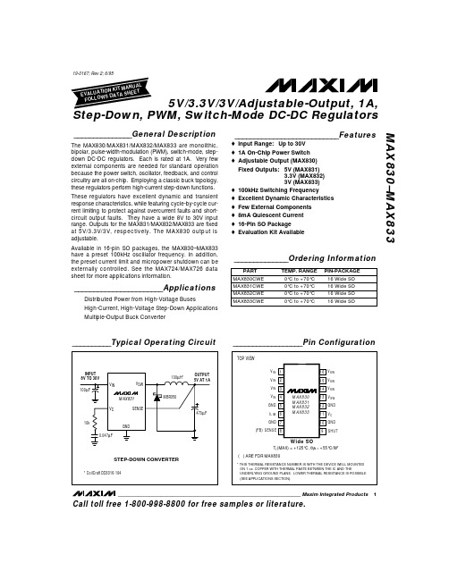
___________________________Features
o Input Range: Up to 30V o 1A On-Chip Power Switch o Adjustable Output (MAX830) Fixed Outputs: 5V (MAX831) 3.3V (MAX832) 3V (MAX833) o 100kHz Switching Frequency o Excellent Dynamic Characteristics o Few External Components o 8mA Quiescent Current o 16-Pin SO Package o Evaluation Kit Available
__________Typical Operating Circuit
__________________Pin Configuration
TOP VIEW
INPUT 8V TO 30V 100µF VIN VSW
100µH*
OUTPUT 5V AT 1A
V IN 1 V IN 2 V IN 3
16 V SW 15 V SW 14 V SW
_______________________Applications
Distributed Power from High-Voltage Buses High-Current, High-Voltage Step-Down Applications Multiple-Output Buck Converter
MAX831
VC 10k 0.047µF SENSE
MAX4636中文资料

元器件交易网
Fast, Low-Voltage, Dual 4Ω SPDT CMOS Analog Switches MAX4635/MAX4636
ABSOLUTE MAXIMUM RATINGS
(Voltages Referenced to GND) V+, IN_ .....................................................................-0.3V to +6V COM_, NC_, NO_ (Note 1) .......................... -0.3V to (V+ + 0.3V) Continuous Current into Any Terminal .............................±30mA Peak Current into COM_, NC_, NO_ (pulsed at 1ms, 10% duty cycle).................................±100mA Continuous Power Dissipation (TA = +70°C) 10-Pin µMAX (derate 4.7mW/°C above +70°C) ............330mW 10-Pin Thin QFN (derate 24.4mW/°C above +70°C) ..1951mW Operating Temperature Range .......................... -40°C to +85°C Storage Temperature Range ........................... -65°C to +150°C Lead Temperature (soldering, 10s) ............................... +300°C
常用模拟开关芯片型号与功能和应用介绍

常用模拟开关芯片型号与功能和应用介绍
1.CD4066:
CD4066是一种四路双开关模拟集成电路。
它可以用作高速CMOS开关、模拟信号开关和数字信号开关。
CD4066具有低电平阈值和高通串脉冲响
应等特性,可以通过外部电压来控制其开关状态。
其应用包括模拟开关、
数据路由、模拟选择器和模拟交换等。
2.MAX4617:
MAX4617是一种低电阻四路双开关。
它具有低电阻和低电平失真的特点,可用于模拟交换、模拟多路复用和模拟电流控制等应用。
MAX4617还
具有高速开关时间和广泛的供电电压范围,适用于多种电路设计。
3.ADG601:
ADG601是一种单路、高精度CMOS模拟开关芯片。
它具有低电位失真、低电流和低电压操作的特点,适用于音频信号开关、电量计选择、过程控
制和自动测试设备等应用。
ADG601还具有低串扰和低抖动等特性,可以
提供高品质的信号传输。
这些模拟开关芯片的功能和应用广泛,可以满足不同领域的需求。
它
们在信号传输、数据交换、功率控制和信号处理等方面发挥着重要作用。
无论是工业自动化、通信设备、消费电子产品还是医疗设备,这些模拟开
关芯片都能够提供可靠和精确的信号控制。
因此,选取适合的模拟开关芯
片对于电路设计和系统性能至关重要。
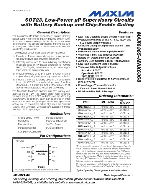
MAX6365PKA46+T中文资料

General DescriptionThe MAX6365–MAX6368 supervisory circuits simplify power-supply monitoring, battery-backup control func-tions, and memory write protection in microprocessor (µP) systems. The circuits significantly improve the size,accuracy, and reliability of modern systems with an ultra-small integrated solution.These devices perform four basic system functions:1) Provide a µP reset output during V CC supply power-up, power-down, and brownout conditions.2) Internally control V CC to backup-battery switching tomaintain data or low-power operation for CMOS RAM, CMOS µPs, real-time clocks, and other digital logic when the main supply fails.3) Provide memory write protection through internalchip-enable gating during supply or processor faults.4) Include one of the following options: a manual resetinput (MAX6365), a watchdog timer function (MAX6366), a battery-on output (MAX6367), or an auxiliary user-adjustable reset input (MAX6368).The MAX6365–MAX6368 operate from V CC supply volt-ages as low as 1.2V. The factory preset reset threshold voltages range from 2.32V to 4.63V (see the Ordering Information ). In addition, each part is offered in three reset output versions: push-pull active low, open-drain active low, or open-drain active high (see the Selector Guide ). The MAX6365–MAX6368 are available in minia-ture 8-pin SOT23 packages.ApplicationsCritical µP/µC Power Portable/Battery-Monitoring Powered Equipment Fax Machines Set-Top Boxes Industrial Control POS EquipmentComputers/ControllersFeatures♦Low +1.2V Operating Supply Voltage (V CC or V BATT )♦Precision Monitoring of +5.0V, +3.3V, +3.0V, and +2.5V Power-Supply Voltages♦On-Board Gating of Chip-Enable Signals, 1.5ns Propagation Delay♦Debounced Manual Reset Input (MAX6365)♦Watchdog Timer, 1.6s Timeout (MAX6366)♦Battery-On Output Indicator (MAX6367)♦Auxiliary User-Adjustable RESET IN (MAX6368)♦Low 10µA Quiescent Supply Current ♦Three Available Output StructuresPush-Pull RESET Open-Drain RESET Open-Drain RESET♦RESET/RESET Valid Down to 1.2V Guaranteed (V CC or V BATT )♦Power-Supply Transient Immunity ♦150ms min Reset Timeout Period ♦Miniature 8-Pin SOT23 PackageMAX6365–MAX6368SOT23, Low-Power µP Supervisory Circuits with Battery Backup and Chip-Enable Gating________________________________________________________________Maxim Integrated Products1Pin Configurations19-1658; Rev 3; 12/05For pricing, delivery, and ordering information,please contact Maxim/Dallas Direct!at 1-888-629-4642, or visit Maxim’s website at .Ordering Information*These parts offer a choice of reset threshold voltages. From the Reset Threshold Ranges table, insert the desired threshold volt-age code in the blank to complete the part number. SOT parts come in tape-and-reel only and must be ordered in 2500-piece increments. See Device Marking Codes for a complete parts list,including SOT top marks and standard threshold versions. See Selector Guide for a listing of device features.Devices are available in both leaded and lead-free packaging.Specify lead-free by replacing “-T” with “+T” when ordering.Typical Operating Circuit appears at end of data sheet.M A X 6365–M A X 6368SOT23, Low-Power µP Supervisory Circuits with Battery Backup and Chip-Enable GatingABSOLUTE MAXIMUM RATINGSELECTRICAL CHARACTERISTICS(V = +2.4V to +5.5V, V = +3.0V, CE IN = V , reset not asserted, T = -40°C to +85°C. Typical values are at T = +25°C,Stresses beyond those listed under “Absolute Maximum Ratings” may cause permanent damage to the device. These are stress ratings only, and functional operation of the device at these or any other conditions beyond those indicated in the operational sections of the specifications is not implied. Exposure to absolute maximum rating conditions for extended periods may affect device reliability.Terminal Voltages (with respect to GND)V CC , BATT, OUT.......................................................-0.3V to +6V RESET (open drain), RESET (open drain)................-0.3V to +6V BATT ON, RESET (push-pull), RESET IN,WDI, CE IN, CE OUT...........................-0.3V to (V OUT + 0.3V)MR ..............................................................-0.3V to (V CC + 0.3V)Input CurrentV CC Peak ..............................................................................1A V CC Continuous.............................................................250mA BATT Peak.....................................................................250mA BATT Continuous.............................................................40mAGND...............................................................................75mA Output CurrentOUT...............................Short-Circuit Protected for up to 10s RESET, RESET , BATT ON, CE OUT...............................20mA Continuous Power Dissipation (T A = +70°C)8-Pin SOT23 (derate 8.75mW/°C above +70°C)........700mW Operating Temperature Range ...........................-40°C to +85°C Storage Temperature Range.............................-65°C to +150°C Junction Temperature .....................................................+150°C Lead Temperature (soldering, 10s).................................+300°CMAX6365–MAX6368SOT23, Low-Power µP Supervisory Circuits with Battery Backup and Chip-Enable Gating_______________________________________________________________________________________3ELECTRICAL CHARACTERISTICS (continued)(V CC = +2.4V to +5.5V, V BATT = +3.0V, CE IN = V CC , reset not asserted, T A = -40°C to +85°C. Typical values are at T A = +25°C,M A X 6365–M A X 6368SOT23, Low-Power µP Supervisory Circuits with Battery Backup and Chip-Enable Gating 4_______________________________________________________________________________________Typical Operating Characteristics(T A = +25°C, unless otherwise noted.)8109121115141316-400-2020406080SUPPLY CURRENTvs. TEMPERATURE (NO LOAD)TEMPERATURE (°C)S U P P L Y C U R R E N T (µA )0.20.60.40.81.01.2BATTERY SUPPLY CURRENT (BACKUP MODE) vs. TEMPERATURETEMPERATURE (°C)B A T T E R Y S U P P L YC U R R E N T (µA )-402040-200608021437658-40-2020406080BATT-TO-OUT ON-RESISTANCEvs. TEMPERATURETEMPERATURE (°C)B A T T -T O -O U T O N -R E S I S T A NC E (Ω)ELECTRICAL CHARACTERISTICS (continued)(V= +2.4V to +5.5V, V = +3.0V, CE IN = V , reset not asserted, T = -40°C to +85°C. Typical values are at T = +25°C,Note 2:V BATT can be 0 anytime, or V CC can go down to 0 if V BATT is active (except at startup).Note 3:RESET is pulled up to OUT. Specifications apply for OUT = V CC or OUT = BATT.Note 4:The chip-enable resistance is tested with V CC = V TH(MAX)and CE IN = V CC / 2.MAX6365–MAX6368SOT23, Low-Power µP Supervisory Circuits with Battery Backup and Chip-Enable Gating_______________________________________________________________________________________5Typical Operating Characteristics (continued)(T A = +25°C, unless otherwise noted.)00.40.20.80.61.21.01.4-4020-20406080V CC TO OUT ON-RESISTANCEvs. TEMPERATURETEMPERATURE (°C)V C C T O O U T O N -R E S I S T A N C E (Ω)190195205200210RESET TIMEOUT PERIOD vs. TEMPERATUREM A X 6365/8-05TEMPERATURE (°C)R E S E T T I M E O U T P E R I O D (m s )-402040-206080301575604513512010590TEMPERATURE (°C)P R O P A G A T I O N D E L A Y (µs )-402040-206080V CC TO RESET PROPAGATION DELAYvs. TEMPERATURE2.03.02.55.04.54.03.5RESET THRESHOLD vs. TEMPERATURETEMPERATURE (°C)T H R E S H O L D (V )-402040-206080110010100010,000MAXIMUM TRANSIENT DURATION vs. RESET THRESHOLD OVERDRIVERESET THRESHOLD OVERDRIVE V TH - V CC (mV)M A X I M U M T R A N S I E N T D U R A T I O N (µs )40030035025020005015010003215498761000.5 1.0 1.5 2.0 2.5 3.03.5BATTERY SUPPLY CURRENT vs. SUPPLY VOLTAGEV CC (V)B A T T E R Y S U P P L YC U R R E N T (µA )M A X 6365–M A X 6368SOT23, Low-Power µP Supervisory Circuits with Battery Backup and Chip-Enable Gating 6_______________________________________________________________________________________1.2341.2351.236MAX6368RESET IN THRESHOLD vs. TEMPERATUREM A X 6365/8 -10TEMPERATURE (°C)V R T H (V )-402040-2060801.01.91.61.32.82.52.2MAX6368RESET IN TO RESET PROPAGATION DELAYvs. TEMPERATURETEMPERATURE (°C)P R O P A G A T I O N D E L A Y (µs )-402040-206080013245C LOAD (pF)P R O P A G A T I O N D E L A Y (n s )10050150200CHIP-ENABLE PROPAGATION DELAY vs. CE OUT LOAD CAPACITANCE515102025-40-2020406080TEMPERATURE (°C)C E I N T O C E O U T O N -R E S I S T A N C E (Ω)CE IN TO CE OUT ON-RESISTANCEvs. TEMPERATURE1.01.31.21.11.51.41.91.81.71.62.0-40-2020406080TEMPERATURE (°C)W A T C H D O G T I M E O U T P E R I O D (s )MAX6366WATCHDOG TIMEOUT PERIODvs. TEMPERATURETypical Operating Characteristics (continued)(T A = +25°C, unless otherwise noted.)MAX6365–MAX6368SOT23, Low-Power µP Supervisory Circuits with Battery Backup and Chip-Enable Gating_______________________________________________________________________________________7M A X 6365–M A X 6368SOT23, Low-Power µP Supervisory Circuits with Battery Backup and Chip-Enable Gating 8_______________________________________________________________________________________Detailed DescriptionThe Typical Operating Circuit shows a typical connec-tion for the MAX6365–MAX6368. OUT powers the static random-access memory (SRAM). If V CC is greater than the reset threshold (V TH ), or if V CC is lower than V TH but higher than V BATT , V CC is connected to OUT. If V CC is lower than V TH and V CC is less than V BATT ,BATT is connected to OUT. OUT supplies up to 150mA from V CC . In battery-backup mode, an internal MOSFET connects the backup battery to OUT. The on-resistance of the MOSFET is a function of backup-battery voltage and is shown in the BATT-to-OUT On-Resistance vs.Temperature graph in the T ypical Operating Char-acteristics .Chip-Enable Signal GatingThe MAX6365–MAX6368 provide internal gating of CE signals to prevent erroneous data from being written toCMOS RAM in the event of a power failure. During nor-mal operation, the CE gate is enabled and passes all CE transitions. When reset asserts, this path becomes disabled, preventing erroneous data from corrupting the CMOS RAM. All of these devices use a series trans-mission gate from CE IN to CE OUT. The 2ns propaga-tion delay from CE IN to CE OUT allows the devices to be used with most µPs and high-speed DSPs.During normal operation, CE IN is connected to CE OUT through a low on-resistance transmission gate.This is valid when reset is not asserted. If CE IN is high when reset is asserted, CE OUT remains high regard-less of any subsequent transitions on CE IN during the reset event.If CE IN is low when reset is asserted, CE OUT is held low for 12µs to allow completion of the read/write oper-ation (F igure 1). After the 12µs delay expires, the CEFunctional DiagramMAX6365–MAX6368SOT23, Low-Power µP Supervisory Circuits with Battery Backup and Chip-Enable Gating_______________________________________________________________________________________9OUT goes high and stays high regardless of any sub-sequent transitions on CE IN during the reset event.When CE OUT is disconnected from CE IN, CE OUT is actively pulled up to OUT.The propagation delay through the chip-enable circuit-ry depends on both the source impedance of the drive to CE IN and the capacitive loading at CE OUT. The chip-enable propagation delay is production tested from the 50% point of CE IN to the 50% point of CE OUT, using a 50Ωdriver and 50pF load capacitance.Minimize the capacitive load at CE OUT to minimize propagation delay, and use a low-output-impedance driver.Backup-Battery SwitchoverIn a brownout or power failure, it may be necessary to preserve the contents of the RAM. With a backup bat-tery installed at BATT, the MAX6365–MAX6368 auto-matically switch the RAM to backup power when V CC falls. The MAX6367 has a BATT ON output that goes high in battery-backup mode. These devices require two conditions before switching to battery-backup mode:1) V CC must be below the reset threshold.2) V CC must be below V BATT .Table 1 lists the status of the inputs and outputs in bat-tery-backup mode. The devices do not power up if the only voltage source is on BATT. OUT only powers upfrom V CC at startup.Many µP-based products require manual reset capabili-ty, allowing the user or external logic circuitry to initiate a reset. For the MAX6365, a logic low on MR asserts reset.Reset remains asserted while MR is low and for a mini-mum of 150ms (t RP ) after it returns high. MR has an inter-nal 20k Ωpullup resistor to V CC . This input can be driven with TTL/CMOS logic levels or with open-drain/collector outputs. Connect a normally open momentary switch from MR to GND to create a manual reset function; exter-nal debounce circuitry is not required. If MR is driven from long cables or the device is used in a noisy environ-ment, connect a 0.1µF capacitor from MR to GND to pro-vide additional noise immunity.Figure 1. Reset and Chip-Enable TimingM A X 6365–M A X 6368SOT23, Low-Power µP Supervisory Circuits with Battery Backup and Chip-Enable Gating 10______________________________________________________________________________________Watchdog Input (MAX6366 Only)The watchdog monitors µP activity through the watch-dog input (WDI). If the µP becomes inactive, reset asserts. To use the watchdog function, connect WDI to a bus line or µP I/O line. A change of state (high to low,low to high, or a minimum 100ns pulse) resets the watchdog timer. If WDI remains high or low for longer than the watchdog timeout period (t WD ), the internal watchdog timer runs out and a reset pulse is triggered for the reset timeout period (t RP ). The internal watchdog timer clears whenever reset asserts or whenever WDI sees a rising or falling edge. If WDI remains in either a high or low state, a reset pulse asserts periodically after every t WD (Figure 2).BATT ON Indicator (MAX6367 Only)BATT ON is a push-pull output that drives high when in battery-backup mode. BATT ON typically sinks 3.2mA at 0.1V saturation voltage. In battery-backup mode, this terminal sources approximately 10µA from OUT. Use BATT ON to indicate battery-switchover status or to supply base drive to an external pass transistor for higher current applications (Figure 3).RESET IN Comparator (MAX6368 Only)RESET IN is compared to an internal 1.235V reference.If the voltage at RESET IN is less than 1.235V, reset asserts. Use the RESET IN comparator as an undervolt-age detector to signal a failing power supply or as a secondary power-supply reset monitor.To program the reset threshold (V RTH ) of the secondary power supply, use the following (see Typical Operating Circuit ):V RTH = V REF (R1 / R2 + 1)where V REF = 1.235V. To simplify the resistor selection,choose a value for R2 and calculate R1:R1 = R2 [(V RTH / V REF ) - 1]Since the input current at RESET IN is 25nA (max),large values (up to 1M Ω) can be used for R2 with no significant loss in accuracy. For example, in the Typical Operating Circuit , the MAX6368 monitors two supply voltages. To monitor the secondary 5V logic or analog supply with a 4.60V nominal programmed reset thresh-old, choose R2 = 100k Ω, and calculate R1 = 273k Ω.Reset OutputA µP’s reset input starts the µP in a known state. The MAX6365–MAX6368 µP supervisory circuits assert a reset to prevent code-execution errors during power-up, power-down, and brownout conditions. RESET is guaranteed to be a logic low or logic high, depending on the device chosen (see the Ordering Information ).RESET or RESET asserts when V CC is below the reset threshold and for at least 150ms (t RP ) after V CC rises above the reset threshold. RESET or RESET also asserts when MR is low (MAX6365) and when RESET IN is less than 1.235V (MAX6368). The MAX6366 watch-dog function will cause RESET (or RESET ) to assert in pulses following a watchdog timeout (Figure 2).Applications InformationOperation Withouta Backup Power SourceThe MAX6365–MAX6368 provide battery-backup func-tions. If a backup power source is not used, connect BATT to GND and OUT to V CC .Watchdog Software ConsiderationsOne way to help the watchdog timer monitor the soft-ware execution more closely is to set and reset the watchdog at different points in the program rather than pulsing the watchdog input periodically. F igure 4shows a flow diagram in which the I/O driving theFigure 2. MAX6366 Watchdog Timeout Period and Reset Active TimeMAX6365–MAX6368SOT23, Low-Power µP Supervisory Circuits with Battery Backup and Chip-Enable Gating______________________________________________________________________________________11watchdog is set low in the beginning of the program,set high at the beginning of every subroutine or loop,and set low again when the program returns to the beginning. If the program should hang in any subrou-tine, the problem would be quickly corrected.Replacing the Backup BatteryWhen V CC is above V TH , the backup power source can be removed without danger of triggering a reset pulse.The device does not enter battery-backup mode when V CC stays above the reset threshold voltage.Negative-Going V CC TransientsThese supervisors are relatively immune to short-dura-tion, negative-going V CC transients. Resetting the µP when V CC experiences only small glitches is usually not desirable.The T ypical Operating Characteristics section has a Maximum Transient Duration vs. Reset Threshold Overdrive graph for which reset is not asserted. The graph was produced using negative-going V CC pulses,starting at V CC and ending below the reset threshold by the magnitude indicated (reset threshold overdrive).The graph shows the maximum pulse width that a neg-ative-going V CC transient can typically have without triggering a reset pulse. As the amplitude of the tran-sient increases (i.e., goes further below the reset threshold), the maximum allowable pulse width decreases. Typically, a V CC transient that goes 100mV below the reset threshold and lasts for 30µs will not trig-ger a reset pulse.A 0.1µF bypass capacitor mounted close to the V CC pin provides additional transient immunity.M A X 6365–M A X 6368SOT23, Low-Power µP Supervisory Circuits with Battery Backup and Chip-Enable Gating 12______________________________________________________________________________________standard versions only. Contact factory for availability of nonstandard versions.MAX6365–MAX6368SOT23, Low-Power µP Supervisory Circuits with Battery Backup and Chip-Enable Gating______________________________________________________________________________________13Pin Configurations (continued)M A X 6365–M A X 6368SOT23, Low-Power µP Supervisory Circuits with Battery Backup and Chip-Enable Gating 14______________________________________________________________________________________Typical Operating CircuitChip InformationTRANSISTOR COUNT: 729PROCESS: CMOSSOT23, Low-Power µP Supervisory Circuits with Battery Backup and Chip-Enable GatingMAX6365–MAX6368Maxim cannot assume responsibility for use of any circuitry other than circuitry entirely embodied in a Maxim product. No circuit patent licenses are implied. Maxim reserves the right to change the circuitry and specifications without notice at any time.Maxim Integrated Products, 120 San Gabriel Drive, Sunnyvale, CA 94086 408-737-7600 ____________________15©2005 Maxim Integrated ProductsPrinted USAis a registered trademark of Maxim Integrated Products, Inc.Package Information(The package drawing(s) in this data sheet may not reflect the most current specifications. For the latest package outline information go to /packages .)。
MAX465中文资料

PART
DESCRIPΒιβλιοθήκη IONMAX463 MAX464 MAX465 MAX466 MAX467 MAX468 MAX469 MAX470
Triple RGB Switch & Buffer Quad RGB Switch & Buffer Triple RGB Switch & Buffer Quad RGB Switch & Buffer Triple Video Buffer Quad Video Buffer Triple Video Buffer Quad Video Buffer
Continuous Power Dissipation (TA = +70°C) 16-Pin Plastic DIP (derate 22.22mW/°C above +70°C) ....1778mW 16-Pin Wide SO (derate 20.00mW/°C above +70°C) .......1600mW
The MAX463–MAX470 series of two-channel, triple/quad buffered video switches and video buffers combines high-accuracy, unity-gain-stable amplifiers with high-performance video switches. Fast switching time and low differential gain and phase error make this series of switches and buffers ideal for all video applications. The devices are all specified for ±5V supply operation with inputs and outputs as high as ±2.5V when driving 150Ω loads (75Ω back-terminated cable).
MAX6368PKA46+T中文资料
VCC Peak ..............................................................................1A VCC Continuous .............................................................250mA BATT Peak .....................................................................250mA
MAX6368HKA_ _-T
-40°C to +85°C
8 SOT23-8
*These parts offer a choice of reset threshold voltages. From the Reset Threshold Ranges table, insert the desired threshold voltage code in the blank to complete the part number. SOT parts come in tape-and-reel only and must be ordered in 2500-piece increments. See Device Marking Codes for a complete parts list, including SOT top marks and standard threshold versions. See Selector Guide for a listing of device features.
MAX6342SUT-T中文资料

MAX6342–MAX6345
6-Pin µP Reset Circuit with Power-Fail Comparator
ABSOLUTE MAXIMUM RATINGS
VCC to GND ..............................................................-0.3V to +6V RESET, RESET
元器件交易网
19-1568; Rev 2; 12/05
MAX6342–MAX6345
6-Pin µP Reset Circuit with Power-Fail Comparator
General Description
The MAX6342–MAX6345 family of microprocessor (µP) supervisory circuits monitors power supplies in digital systems. These devices significantly improve system reliability and accuracy compared to separate ICs or discrete components.
For pricing, delivery, and ordering information, please contact Maxim/Dallas Direct! at 1-888-629-4642, or visit Maxim’s website at .
元器件交易网
Selector Guide 1
SUFFIX
L
M T S R Z
RESET THRESHOLD (V) 4.63 4.38 3.08 2.93 2.63 2.33
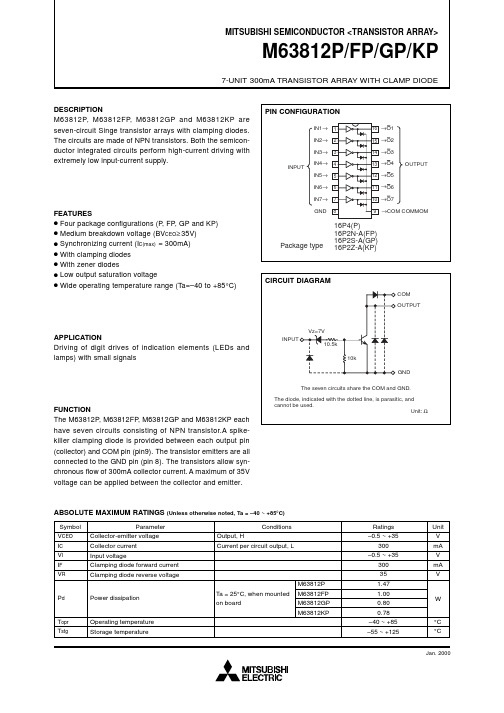
M63812P中文资料
mA
V
ELECTRICAL CHARACTERISTICS (Unless otherwise noted, Ta = 25°C)
Symbol V (BR) CEO VCE(sat) VIN(on) VR IR h FE Parameter Collector-emitter breakdown voltage Test conditions Limits min 35 — — 13 — — 50 typ — — — 19 1.2 — — max — 0.2 0.8 23 2.0 10 — Unit V V V V µA —
GND
→COM COMMOM
Package type
16P4(P) 16P2N-A(FP) 16P2S-A(GP) 16P2Z-A(KP)
CIRCUIT DIAGRAM
COM OUTPUT
Vz=7V
APPLICATION Driving of digit drives of indication elements (LEDs and lamps) with small signals
•The collector current values represent the current per circuit. •Repeated frequency ≥ 10Hz •The value the circle represents the value of the simultaneously-operated circuit. •Ta = 85°C
Thermal Derating Factor Characteristics 2.0
Power dissipation Pd (W)
Input Characteristics 4
- 1、下载文档前请自行甄别文档内容的完整性,平台不提供额外的编辑、内容补充、找答案等附加服务。
- 2、"仅部分预览"的文档,不可在线预览部分如存在完整性等问题,可反馈申请退款(可完整预览的文档不适用该条件!)。
- 3、如文档侵犯您的权益,请联系客服反馈,我们会尽快为您处理(人工客服工作时间:9:00-18:30)。
General Description The MAX6381–MAX6390 microprocessor (µP) supervisory circuits monitor power-supply voltages from +1.8V to +5.0V while consuming only 3µA of supply current at +1.8V. Whenever V CC falls below the factory-set reset thresholds, the reset output asserts and remains assert-ed for a minimum reset timeout period after V CC rises above the reset threshold. Reset thresholds are available from +1.58V to +4.63V, in approximately 100mV incre-ments. Seven minimum reset timeout delays ranging from 1ms to 1200ms are available.The MAX6381/MAX6384/MAX6387 have a push-pull active-low reset output. The MAX6382/MAX6385/ MAX6388 have a push-pull active-high reset output, and the MAX6383/MAX6386/MAX6389/MAX6390 have an open-drain active-low reset output. The MAX6384/MAX6385/MAX6386 also feature a debounced manual reset input (with internal pullup resistor). The MAX6387/MAX6388/MAX6389 have an auxiliary input for monitoring a second voltage. The MAX6390 offers a manual reset input with a longer V CC reset timeout period (1120ms or 1200ms) and a shorter manual reset timeout (140ms or 150ms).The MAX6381/MAX6382/MAX6383 are available in 3-pin SC70 and6-pinµDFN packages and the MAX6384–MAX6390 are available in 4-pin SC70 andFeatures♦Factory-Set Reset Threshold Voltages Rangingfrom +1.58V to +4.63V in Approximately 100mVIncrements♦±2.5% Reset Threshold Accuracy OverTemperature (-40°C to +125°C)♦Seven Reset Timeout Periods Available: 1ms,20ms, 140ms, 280ms, 560ms, 1120ms,1200ms (min)♦3 Reset Output OptionsActive-Low Push-PullActive-High Push-PullActive-Low Open-Drain♦Reset Output State Guaranteed ValidDown to V CC= 1V♦Manual Reset Input (MAX6384/MAX6385/MAX6386)♦Auxiliary RESET IN(MAX6387/MAX6388/MAX6389)♦V CC Reset Timeout (1120ms or 1200ms)/ManualReset Timeout (140ms or 150ms) (MAX6390)♦Negative-Going V CC Transient Immunity♦Low Power Consumption of 6µA at +3.6Vand 3µA at +1.8V♦Pin Compatible withMAX809/MAX810/MAX803/MAX6326/MAX6327/MAX6328/MAX6346/MAX6347/MAX6348,and MAX6711/MAX6712/MAX6713♦Tiny 3-Pin/4-Pin SC70 and 6-Pin µDFN PackagesMAX6381–MAX6390 SC70/µDFN, Single/Dual Low-Voltage,Low-Power µP Reset Circuits ________________________________________________________________Maxim Integrated Products1Pin Configurations19-1839; Rev 4; 4/07Ordering InformationOrdering Information continued at end of data sheet.Typi cal Operati ng Ci rcui t appears at end of data sheet.Selector Guide appears at end of data sheet.after "XR", "XS", or "LT." Insert reset timeout delay (see ResetTimeout Delay table) after "D" to complete the part number.Sample stock is generally held on standard versions only (seeStandard Versions table). Standard versions have an orderincrement requirement of 2500 pieces. Nonstandard versionshave an order increment requirement of 10,000 pieces.Contact factory for availability of nonstandard versions.+Denotes a lead-free package.For pricing, delivery, and ordering information,please contact Maxim Direct at 1-888-629-4642,or visit Maxim’s website at .ComputersControllersIntelligent InstrumentsCritical µP and µCPower MonitoringPortable/Battery-Powered EquipmentDual Voltage SystemsM A X 6381–M A X 6390SC70/µDFN, Single/Dual Low-Voltage, Low-Power µP Reset CircuitsABSOLUTE MAXIMUM RATINGSELECTRICAL CHARACTERISTICS(V CC = full range, T A = -40°C to +125°C, unless otherwise specified. Typical values are at T A = +25°C.) (Note 1)Stresses beyond those listed under “Absolute Maximum Ratings” may cause permanent damage to the device. These are stress ratings only, and functional operation of the device at these or any other conditions beyond those indicated in the operational sections of the specifications is not implied. Exposure to absolute maximum rating conditions for extended periods may affect device reliability.V CC to GND..........................................................-0.3V to +6.0V RESET Open-Drain Output....................................-0.3V to +6.0V RESET , RESET (push-pull output)..............-0.3V to (V CC + 0.3V)MR , RESET IN.............................................-0.3V to (V CC + 0.3V)Input Current (V CC ).............................................................20mA Output Current (all pins).....................................................20mAContinuous Power Dissipation (T A = +70°C)3-Pin SC70 (derate 2.9mW/°C above +70°C)..............235mW 4-Pin SC70 (derate 3.1mW/°C above +70°C)..............245mW 6-Pin µDFN (derate 2.1mW/°C above +70°C)..........167.7mW Operating Temperature Range .........................-40°C to +125°C Storage Temperature Range.............................-65°C to +150°C Lead Temperature (soldering, 10s).................................+300°CMAX6381–MAX6390SC70/µDFN, Single/Dual Low-Voltage,Low-Power µP Reset Circuits_______________________________________________________________________________________3M A X 6381–M A X 6390SC70/µDFN, Single/Dual Low-Voltage, Low-Power µP Reset Circuits 4______________________________________________________________________________________Typical Operating Characteristics(T A = +25°C, unless otherwise noted.)215436789-40-105-25203550658095110125SUPPLY CURRENT vs. TEMPERATURE(NO LOAD)TEMPERATURE (°C)S U P P L Y C U R R E N T (µA )25292735333137394143-40-105-25203550658095110125POWER-DOWN RESET DELAYvs. TEMPERATURETEMPERATURE (°C)P O W E R -D O W N R E S E T D E L A Y (µs )0.940.980.961.021.001.061.041.08-40-10520-253550658095110125NORMALIZED POWER-UP RESET TIMEOUTvs. TEMPERATUREM A X 6381/90 t o c 03TEMPERATURE (°C)N O R M A L I Z E D R E S E T T I M E O U T P E R I O D0.9900.9851.0150.9950.9901.0001.0051.0101.020-40-10520-253550958011065125M A X 6381/90 t o c 04TEMPERATURE (°C)N O R M A L I Z E D R E S E T TH R E S H O L D NORMALIZED RESET THRESHOLDvs. TEMPERATURE00.40.20.80.61.01.2063912OUTPUT-VOLTAGE LOW vs. SINK CURRENTI SINK (mA)V O L (V )01.00.52.01.52.53.00500750250100012501500OUTPUT-VOLTAGE HIGH vs. SOURCE CURRENTI SOURCE (µA)V O H (V )45001100010010MAXIMUM TRANSIENT DURATION vs. RESET COMPARATOR OVERDRIVE15050350250500200100400300RESET COMPARATOR OVERDRIVE, V TH - V CC (mV)M A X I M U M T R A N S I E N T D U R A T I O N (µs )3.53.93.74.54.34.14.74.95.35.15.5-40-105-25203550658095110125RESET IN TO RESET DELAYvs. TEMPERATUREM A X 6381/90 t o c 08TEMPERATURE (°C)R E S E T I N D E L A Y (µs )MAX6381–MAX6390SC70/µDFN, Single/Dual Low-Voltage,Low-Power µP Reset CircuitsPin DescriptionM A X 6381–M A X 6390SC70/µDFN, Single/Dual Low-Voltage, Low-Power µP Reset Circuits 6_______________________________________________________________________________________Detailed DescriptionRESET OutputA µP reset input starts the µP in a known state. These µP supervisory circuits assert reset to prevent code execution errors during power-up, power-down, or brownout conditions.Reset asserts when V CC is below the reset threshold;once V CC exceeds the reset threshold, an internal timer keeps the reset output asserted for the reset timeout period. After this interval, reset output deasserts. Reset output is guaranteed to be in the correct logic state for V CC ≥1V.Manual Reset Input (MAX6384/MAX6385/MAX6386/MAX6390)Many µP-based products require manual reset capabil-ity, allowing the operator, a test technician, or external logic circuitry to initiate a reset. A logic low on MR asserts reset. Reset remains asserted while MR is low,and for the reset active timeout period (t RP ) after MR returns high. This input has an internal 63k Ωpullup resistor (1.56k Ωfor MAX6390), so it can be left uncon-nected if it is not used. MR can be driven with TTL or CMOS logic levels, or with open-drain/collector outputs.Connect a normally open momentary switch from MR to G ND to create a manual-reset function; external debounce circuitry is not required. If MR is driven from long cables or if the device is used in a noisy environ-ment, connecting a 0.1µF capacitor from MR to G ND provides additional noise immunity.RESET IN Comparator(MAX6387/MAX6388/MAX6389)RESET IN is compared to an internal +1.27V reference.If the voltage at RESET IN is less than 1.27V, reset asserts. Use the RESET IN comparator as a user-adjustable reset detector or as a secondary power-sup-ply monitor by implementing a resistor-divider at RESET IN (shown in Figure 1). Reset asserts when either V CC or RESET IN falls below its respective threshold volt-age. Use the following equation to set the threshold:V INTH = V THRST (R1/R2 + 1)where V THRST = +1.27V. To simplify the resistor selec-tion, choose a value of R2 and calculate R1:R1 = R2 [(V INTH /V THRST ) - 1]Since the input current at RESET IN is 50nA (max),large values can be used for R2 with no significant loss in accuracy.___________Applications InformationNegative-Going V CC TransientsIn addition to issuing a reset to the µP during power-up,power-down, and brownout conditions, the MAX6381–MAX6390 are relatively immune to short dura-tion negative-going V CC transients (glitches).The Typical Operating Characteristics section shows the Maximum Transient Durations vs. Reset Comparator Overdrive, for which the MAX6381–MAX6390 do not generate a reset pulse. This graph was generated usinga negative-going pulse applied to V CC , starting above the actual reset threshold and ending below it by the magnitude indicated (reset comparator overdrive). The graph indicates the typical maximum pulse width a neg-ative-going V CC transient may have without causing a reset pulse to be issued. As the magnitude of the tran-sient increases (goes farther below the reset threshold),the maximum allowable pulse width decreases. A 0.1µF capacitor mounted as close as possible to V CC provides additional transient immunity.Ensuring a Valid RESET Output Down to V CC = 0VThe MAX6381–MAX6390 are guaranteed to operate properly down to V CC = 1V. In applications that require valid reset levels down to V CC = 0V, a pulldown resistor to active-low outputs (push/pull only, Figure 2) and a pullup resistor to active-high outputs (push/pull only)will ensure that the reset line is valid while the reset out-put can no longer sink or source current. This schemedoes not work with the open-drain outputs of the MAX6383/MAX6386/MAX6389/MAX6390. The resistor value used is not critical, but it must be small enough not to load the reset output when V CC is above the reset threshold. For most applications, 100k Ωis ade-quate.MAX6381–MAX6390SC70/µDFN, Single/Dual Low-Voltage,Low-Power µP Reset Circuits_______________________________________________________________________________________7M A X 6381–M A X 6390SC70/µDFN, Single/Dual Low-Voltage, Low-Power µP Reset Circuits 8_______________________________________________________________________________________Selector GuideOrdering Information (continued)Note:Insert reset threshold suffix (see Reset Threshold table)after "XR", "XS", or "LT." Insert reset timeout delay (see Reset Timeout Delay table) after "D" to complete the part number.Sample stock is generally held on standard versions only (see Standard Versions table). Standard versions have an order increment requirement of 2500 pieces. Nonstandard versions have an order increment requirement of 10,000 pieces.Contact factory for availability of nonstandard versions.*MAX6390 is available with D4 or D7 timing only.+Denotes a lead-free package.MAX6381–MAX6390SC70/µDFN, Single/Dual Low-Voltage,Low-Power µP Reset Circuits_______________________________________________________________________________________9Chip InformationTRANSISTOR COUNT: 647PROCESS: BiCMOSPin Configurations (continued)M A X 6381–M A X 6390SC70/µDFN, Single/Dual Low-Voltage, Low-Power µP Reset Circuits 10______________________________________________________________________________________Package Information(The package drawing(s) in this data sheet may not reflect the most current specifications. For the latest package outline information,go to /packages .)MAX6381–MAX6390SC70/µDFN, Single/Dual Low-Voltage,Low-Power µP Reset Circuits______________________________________________________________________________________11Package Information (continued)(The package drawing(s) in this data sheet may not reflect the most current specifications. For the latest package outline information,go to /packages .)M A X 6381–M A X 6390SC70/µDFN, Single/Dual Low-Voltage, Low-Power µP Reset Circuits 12______________________________________________________________________________________Package Information (continued)(The package drawing(s) in this data sheet may not reflect the most current specifications. For the latest package outline information,go to /packages .)SC70/µDFN, Single/Dual Low-Voltage,Low-Power µP Reset CircuitsMaxim cannot assume responsibility for use of any circuitry other than circuitry entirely embodied in a Maxim product. No circuit patent licenses are implied. Maxim reserves the right to change the circuitry and specifications without notice at any time.Maxim Integrated Products, 120 San Gabriel Drive, Sunnyvale, CA 94086 408-737-7600____________________13©2007 Maxim Integrated Productsis a registered trademark of Maxim Integrated Products, Inc.MAX6381–MAX6390Package Information (continued)(The package drawing(s) in this data sheet may not reflect the most current specifications. For the latest package outline information,go to /packages .)Revision HistoryPages changed at Rev 4: Title on all pages, 1, 2, 5,7–13。