VASD2-DIP中文资料
2-乙基吡啶

2-乙基吡啶化学品安全技术说明书第一部分:化学品名称化学品中文名称:2-乙基吡啶 化学品英文名称:2-ethylpyridine 中文名称2:α-乙基吡啶 英文名称2:α-ethylpyridine 技术说明书编码:2971CAS No.:100-71-0 分子式:C 7H 9N 分子量:107.16第二部分:成分/组成信息有害物成分含量CAS No.第三部分:危险性概述健康危害:有毒。
对眼睛、皮肤和粘膜有刺激作用。
接触可引起头痛、恶心和呕吐等。
环境危害:对环境有危害。
燃爆危险:本品易燃,具刺激性。
第四部分:急救措施皮肤接触:脱去污染的衣着,用大量流动清水冲洗眼睛接触:提起眼睑,用流动清水或生理盐水冲洗。
就医。
吸入:迅速脱离现场至空气新鲜处。
保持呼吸道通畅。
如呼吸困难,给输氧。
如呼吸停止,立即进行人工呼吸。
就医。
食入:饮足量温水,催吐。
就医。
第五部分:消防措施危险特性:其蒸气与空气可形成爆炸性混合物,遇明火、高热能引起燃烧爆炸。
与氧化剂能发生强烈反应。
受高热分解放出有毒的气体。
若遇高热,容器内压增大,有开裂和爆炸的危险。
有害燃烧产物:一氧化碳、二氧化碳、氮氧化物。
灭火方法:消防人员须佩戴防毒面具、穿全身消防服,在上风向灭火。
尽可能将容器从火场移至空旷处。
喷水保持火场容器冷却,直至灭火结束。
处在火场中的容器若已变色或从安全泄压装置中产生声音,必须马上撤离。
灭火剂:雾状水、泡沫、干粉、二氧化碳、砂土。
第六部分:泄漏应急处理有害物成分 含量 CAS No.:2-乙基吡啶 100-71-0应急处理:迅速撤离泄漏污染区人员至安全区,并进行隔离,严格限制出入。
切断火源。
建议应急处理人员戴自给式呼吸器,穿全棉防毒服。
不要直接接触泄漏物。
尽可能切断泄漏源。
防止流入下水道、排洪沟等限制性空间。
小量泄漏:用砂土或其它不燃材料吸附或吸收。
大量泄漏:构筑围堤或挖坑收容。
用泵转移至槽车或专用收集器内,回收或运至废物第七部分:操作处置与储存操作注意事项:密闭操作,局部排风。
V2DIP1-32;中文规格书,Datasheet资料

Future Technology Devices International Ltd (FTDI)Unit 1, 2 Seaward Place, Centurion Business Park, Glasgow, G41 1HH, United KingdomTel.: +44 (0) 141 429 2777 Fax: + 44 (0) 141 429 2758E-Mail (Support): support1@Web: Neither the whole nor any part of the information contained in, or the product described in this manual, may be adapted or reproduced in any material or electronic form without the prior written consent of the copyright holder. This product and its documentation are supplied on an as-is basis and no warranty as to their suitability for any particular purpose is either made or implied. Future Technology Devices International Ltd will not accept any claim for damages howsoever arising as a result of use or failure of this product. Your statutory rights are not affected. This product or any variant of it is not intended for use in any medical appliance, device or system in which the failure of the product might reasonably be expected to result in personal injury. This document provides preliminary information that may be subject to change without notice. No freedom to use patents or other intellectual property rights is implied by the publication of this document. Future Technology Devices International Ltd, Unit 1, 2 Seaward Place, Centurion Business Park,Future Technology Devices International Ltd.V2DIP1-32VNC2-32Q Development ModuleDatasheetDocument Reference No.: FT_000163Version 1.01Issue Date: 2010-05-251IntroductionV2DIP1-32 module is designed to allow rapid development of designs using the VNC2-32Q IC. The V2DIP1-32 is supplied as a PCB designed to fit into a 24 pin 0.6” wide / 0.1” pitch DIP socket. The module provides access to the UART, parallel FIFO and SPI interface pins of the VNC2-32Q device via its IO bus pins. The USB port is accessed via a type A USB connector.Figure 1.1 - V2DIP1-32The VNC2 is the second of F TDI’s Vinculum family of Embedded dual USB host controller devices. The VNC2 device provides USB Host interfacing capability for a variety of different USB device classes including support for BOMS (bulk only mass storage), Printer, HID (human interface devices). For mass storage devices such as USB Flash drives, VNC2 also transparently handles the FAT file structure. Communication with non USB devices such as a low cost microcontroller is accomplished via either UART, SPI or parallel FIFO interfaces. The VNC2 provides a new cost effective solution for providing USB Host capability into products that previously did not have the hardware resources available.The VNC2 supports the capability to enable customers to develop custom firmware using the Vinculum II development software tool suite. The development tools support compiler, linker and debugger tools complete within an integrated development environment (IDE).The Vinculum-II VNC2 family of devices are available in Pb-free (RoHS compliant) 32-lead LQFP, 32-leadTable of Contents1Introduction (1)2Features (3)3Pin Out and Signal Description (4)3.1Module Pin Out (4)3.2Pin Signal Description (6)3.3Default Interface I/O Pin Configuration (7)3.4UART Interface (8)3.4.1Signal Description – UART Interface (8)3.5Serial Peripheral Interface (SPI) (9)3.5.1Signal Description - SPI Slave (9)3.5.2Signal Description - SPI Master (9)3.6Parallel FIFO Interface - Asynchronous Mode (10)3.6.1Signal Description - Parallel FIFO Interface (10)3.6.2Timing Diagram – Asynchronous FIFO Mode Read and Write Cycle (11)3.7Debugger Interface (12)3.7.1Signal Description - Debugger Interface (12)4Firmware (13)4.1Firmware Support (13)4.2Available Firmware (13)4.3Firmware Upgrades (13)5External circuit Configuration (14)5.1Adding a second USB Port (14)6Mechanical Dimensions (15)7Schematic Diagram (16)8Contact Information (17)Appendix A – References (18)Appendix B – List of Figures and Tables (19)List of Figures (19)List of Tables (19)Appendix C – Revision History (20)2FeaturesThe V2DIP1-32 incorporates the following features:Uses FTDI’s VNC2-32Q embedded USB host controller IC device.USB ‘A’ type USB socket to interface with USB peripheral devices.Second USB interface port accessible via module pins if required.UART, parallel FIFO and SPI interfaces can be programmed to a choice of available I/O pins. Single 5V supply input from DIL connectors or 5V supplied via USB VBUS slave interface or debugger module.Auxiliary 3.3 V / 200 mA power output to external logic. All VNC2 signals available on 0.6” wi de / 0.1” pitch DIL male connectors.Power and traffic indicator LED’s.V2DIP1-32 is a Pb-free, RoHS compliant development module.Debugger interface pin available on DIL pins or via 6 way male header which interfaces to separate debugger module.Firmware upgrades via UART or debugger interface pin headerFOC software development suite of tools to create customised firmware includes a Compiler, Linker,Debugger and Assembler all wrapped up in an easy to use Integrated Design Environment GUI.3Pin Out and Signal Description 3.1Module Pin OutFigure 3.1 - V2DIP1-32 Module Pin Out (Top View)3.2Pin Signal DescriptionTable 3.1 - Pin Signal Descriptions3.3Default Interface I/O Pin ConfigurationThe 32 pin QFN VNC2-32Q device is delivered without any firmware pre-loaded. As such the IOMUX will provide a default pinout as shown in the following table:3.4UART InterfaceWhen the data and control buses are configured in UART mode, the interface implements a standard asynchronous serial UART port with flow control. The UART can support baud rates from 300 baud to3Mbaud. The UART interface is described more fully in the VNC2 datasheet please refer to:- FTDI website3.4.1Signal Description – UART InterfaceThe UART signals can be programmed to a choice of available I/O pins. Table 3.3 explains the available pins for each of the UART signals.3.5Serial Peripheral Interface (SPI)The VNC2-32Q has one SPI master module and two SPI slave modules. These modules are described more fully in a VNC2 datasheet please refer to:- FTDI website3.5.1Signal Description - SPI SlaveThe SPI Slave signals can be programmed to a choice of available I/O pins. Table 3.4explains the available pins for each of the SPI Slave signals.3.5.2Signal Description - SPI MasterThe SPI Master signals can be programmed to a choice of available I/O pins.Table 3.5 shows the SPI master signals and the available pins that they can be mapped.分销商库存信息: FTDIV2DIP1-32。
半导体二极管基本知识

半导体二极管基本知识1概述二极管又称晶体二极管,简称二极管(diode),半导体二极管是指利用半导体特性的两端电子器件。
最常见的半导体二极管是PN结型二极管和金属半导体接触二极管。
它们的共同特点是伏安特性的不对称性,即电流沿其一个方向呈现良好的导电性,而在相反方向呈现高阻特性。
可用作为整流、检波、稳压、恒流、变容、开关、发光及光电转换等。
利用高掺杂PN结中载流子的隧道效应可制成超高频放大或超高速开关的隧道二极管。
2结构PN结两端各引出一个电极并加上管壳,就形成了半导体二极管。
PN结的P型半导体一端引出的电极称为阳极,PN结的N型半导体一端引出的电极称为阴极。
半导体二极管按结构不同可分为点接触型、面接触型和平面型。
图1 二极管结构示意图及电路符号2.1点接触型半导体二极管由一根金属丝与半导体表面相接触,经过特殊工艺,在接触点上形成PN结,作出引线,加上管壳封装而成,见图2。
点接触型二极管的PN结面积小,高频性能好,适用于高频检波电路、开关电路。
图2 点接触型二极管示意图2.2面接触型半导体二极管,它的PN结是用合金法工艺制作而成的,见图3。
面接触型二极管的PN结面积大,可通过较大的电流,一般用于低频整流电路中。
图3 面接触型二极管示意图2.3平面型半导体二极管,它的PN结是用扩散法工艺制作的,见图4。
平面型二极管常用硅平面开关管,其PN结面积较大时,适用于大功率整流;其PN结面积较小时,适用于脉冲数字电路中做开关管使用。
图4 平面型二极管示意图2.4台面型半导体二极管,PN结的制作方法虽然与扩散型相同,但是,只保留PN结及其必要的部分,把不必要的部分用药品腐蚀掉。
其剩余的部分便呈现出台面形,因而得名。
初期生产的台面型,是对半导体材料使用扩散法而制成的。
因此,又把这种台面型称为扩散台面型。
对于这一类型来说,似乎大电流整流用的产品型号很少,而小电流开关用的产品型号却很多。
3主要参数3.1二极管(通用)开启电压V on:使二极管开始导通的临界电压称为开启电压V on。
VIPER22ADIP;VIPER22AS;中文规格书,Datasheet资料

ABSOLUTE MAXIMUM RATINGS
Symbol VDS(sw) VDS(st) ID VDD IFB VESD Tj Tc Tstg Parameter Switching Drain Source Voltage (Tj=25 ... 125°C) Start Up Drain Source Voltage (Tj=25 ... 125°C) Continuous Drain Current Supply Voltage Feedback Current Electrostatic Discharge: Machine Model (R=0Ω; C=200pF) Charged Device Model Junction Operating Temperature Case Operating Temperature Storage Temperature (See note 1) (See note 2) Value -0.3 ... 730 -0.3 ... 400 Internally limited 0 ... 50 3 200 1.5 Internally limited -40 to 150 -55 to 150 Unit V V A V mA V kV °C °C °C
DESCRIPTION The VIPer22A combines a dedicated current mode PWM controller with a high voltage Power BLOCK DIAGRAM
O
bs
t e l o
VDD FB
r P e
INTERNAL SUPPLY _ 8/14.5V + + 42V _
PACKAGE
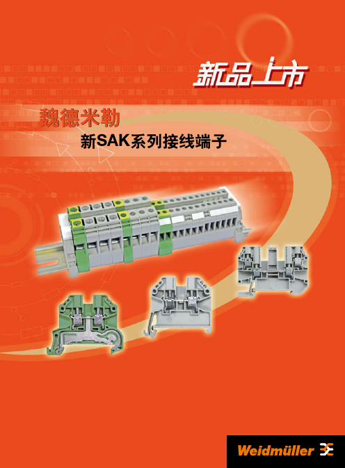
SAKDU接线端子样本
订货号 1129350000 1129370000 1129380000 1129390000
数量 50 50 50 20
订货号 0545400000 0545300000 0546000000
订货号 1129470000
数量 10 10 10
数量 20
型号 SAKQ 10/2 SAKQ 10/3 SAKQ 10/4 SAKQ 10/10
技术参数
额定参数 额定电压 额定电流 额定压接面积 额定冲击电压/污染等级 测量规根据IEC947-1/阻燃等级根据UL94
压接的导线 单股硬导线/多股硬导线 软导线/带管状端头的软导线 压接时的拧紧扭矩 剥线长度/螺丝刀尺寸
压接两根截面积相同的导线 单股硬导线/多股硬导线 软导线/带管状端头的软导线
1129450000
50
型号 SD 0.6X3.5
订货号 9008330000
型号
订货号
SAKEW 35
1129450000
数量 1
数量 50
型号
订货号
DEK 5/5.5 PLUS MC NE
1125030000
数量 1000
型号 DEK 5/6 PLUS MC NE WS
订货号 1011320000
魏德米勒电联接国际贸易(上海)有限公司成立于2001年7月,是魏德米勒集团服务于中国 市场的销售服务机构,拥有覆盖全国的销售网络和完善的售后服务体系,全国设有15个 销售办事处,可以为中国市场的客户提供专业的行业应用解决方案和优质的产品。同时 在上海外高桥保税区,魏德米勒拥有一个超过4,000平方米的物流仓储中心和产品加工中 心,满足客户的实际需求。
15.9/52/59 125/35 2.5…35
DIODES 齐纳二极管常用型号
AZ23C13 AZ23C15 AZ23C16 AZ23C18 AZ23C18W AZ23C20 AZ23C22 AZ23C24 AZ23C27 AZ23C2V7 AZ23C30 AZ23C33 AZ23C36 AZ23C39 AZ23C3V0 AZ23C3V3 AZ23C3V6 AZ23C3V9 AZ23C43 AZ23C47 AZ23C4V3 AZ23C4V7 AZ23C51 AZ23C5V1 AZ23C5V6 AZ23C5V6W AZ23C6V2 AZ23C6V8 AZ23C6V8W AZ23C7V5 AZ23C8V2 AZ23C9V1 BZT52B15LP BZT52C10 BZT52C10LP BZT52C10S BZT52C10T BZT52C10TQ BZT52C11 BZT52C11LP BZT52C11S BZT52C11T BZT52C11TQ BZT52C12 BZT52C12LP BZT52C12S BZT52C12T BZT52C12TQ BZT52C13 BZT52C13LP BZT52C13LPQ BZT52C13S BZT52C13T BZT52C13TQ BZT52C15 BZT52C15LP BZT52C15LPQ BZT52C15S BZT52C15T
深圳市捷比信实业有限公司将DIODES美台齐纳二极管产品型号整理如下: 1SMB5913B 1SMB5914B 1SMB5915B 1SMB5916B 1SMB5917B 1SMB5920B 1SMB5921B 1SMB5922B 1SMB5923B 1SMB5924B 1SMB5925B 1SMB5926B 1SMB5927B 1SMB5928B 1SMB5929B 1SMB5930B 1SMB5931B 1SMB5932B 1SMB5933B 1SMB5934B 1SMB5935B 1SMB5936B 1SMB5937B 1SMB5938B 1SMB5939B 1SMB5940B 1SMB5941B 1SMB5942B 1SMB5943B 1SMB5944B 1SMB5945B 1SMB5946B 1SMB5947B 1SMB5948B 1SMB5949B 1SMB5950B 1SMB5951B 1SMB5952B 1SMB5953B 1SMB5954B 1SMB5955B 1SMB5956B AZ23C10 AZ23C10W AZ23C11 AZ23C12
二正丙胺-危险化学品安全技术说明书中文MSDS文档16个部分(完整版)

化学品安全技术说明书二正丙胺第一部分化学品及企业标识化学品中文名:二正丙胺化学品英文名:dipropylamine; di-n-propylamine供应商名称:天津****化工有限公司供应商地址:天津市**区**路**号**室供应商电话:4571-5858****邮编:248***供应商传真:4571-5858****电子邮件地址:4527**************产品推荐及限制用途:用作有机合成中间体,及溶剂。
第二部分危险性概述紧急情况概述:高度易燃液体和蒸气,吞咽有害,皮肤接触有害,吸入有害,造成严重的皮肤灼伤和眼损伤。
GHS危险性类别:易燃液体-类别2;皮肤腐蚀/刺激-类别1;严重眼损伤/眼刺激-类别1;特异性靶器官毒性-一次接触-类别3(呼吸道刺激)标签要素:象形图:警示词:危险危险信息:H225:高度易燃液体和蒸气H314:造成严重的皮肤灼伤和眼损伤H335:可能引起呼吸道刺激防范说明:预防措施:P210:远离热源/火花/明火/热表面。
禁止吸烟。
P233:保持容器密闭。
P240:容器和接收设备接地/等势联接。
P241:使用防爆的电气/通风/照明/……/设备。
P242:只能使用不产生火花的工具。
P243:采取防止静电放电的措施。
P280:戴防护手套/穿防护服/戴防护眼罩/戴防护面具。
P260:不要吸入粉尘/烟/气体/烟雾/蒸气/喷雾。
P264:作业后彻底清洗……。
P271:只能在室外或通风良好之处使用。
应急响应:P303+P361+P353:如皮肤(或头发)沾染:立即脱掉所有沾染的衣服。
用水清洗皮肤/淋浴。
P370+P378:火灾时,使用……灭火。
P301+P330+P331:如误吞咽:漱口。
不要诱导呕吐。
P363:沾染的衣服清洗后方可重新使用。
P304+P340:如误吸入:将受害人转移到空气新鲜处,保持呼吸舒适的休息姿势。
P310:立即呼叫解毒中心/医生。
P321:具体治疗(见本标签上的.....)。
VBSD1-DIP中文资料

features·isolated 1 W output·temperature range: -40°C~+85°C ·unregulated·high efficiency to 80%·single voltage output ·small footprint ·DIP package style·industry standard pinout ·UL94-V0 package ·no heatsink required ·1K Vdc isolation·power density 0.85 W/cm³·no external component required ·low costdescriptionDesigned to convert fixed volt-ages into an isolated voltage, the VBSD1-DIP series is well suited for providing board-mount local supplies in a wide range of appli-cations, including mixedanalog/digital circuits, test &measurement equip.,process/machine controls, data-com/telecom fields, etc...The semi-regulated output can be followed by 3-terminal regulators to provide output protection, in addition to output regulation.MODELinput voltage output voltageoutput current efficiencynominal range (V dc)max.min.typ.UL60950-1(V dc)(V dc)(mA)(mA)(%)VBSD1-S3.3-S3.3-DIP 3.3 3.00~3.60 3.33033172NO VBSD1-S3.3-S5-DIP 3.3 3.00~3.6052002073NO VBSD1-S5-S3.3-DIP 5 4.5~5.551001068NO VBSD1-S5-S5-DIP 5 4.5~5.552002070YES VBSD1-S5-S9-DIP 5 4.5~5.591111278YES VBSD1-S5-S12-DIP 5 4.5~5.51283978YES VBSD1-S5-S15-DIP 5 4.5~5.51567780YES VBSD1-S12-S3.3-DIP 1210.8~13.2 3.33033173NO VBSD1-S12-S5-DIP 1210.8~13.252002071YES VBSD1-S12-S9-DIP 1210.8~13.291111276YES VBSD1-S12-S12-DIP 1210.8~13.21283978YES VBSD1-S12-S15-DIP 1210.8~13.21567779YES VBSD1-S15-S3.3-DIP 1513.5~16.5 3.33033173NO VBSD1-S15-S5-DIP 1513.5~16.552002074NO VBSD1-S15-S9-DIP 1513.5~16.591111275NO VBSD1-S15-S12-DIP 1513.5~16.51283979NO VBSD1-S15-S15-DIP 1513.5~16.51567775NO VBSD1-S24-S3.3-DIP 2421.6~26.4 3.33033176NO VBSD1-S24-S5-DIP 2421.6~26.452002073YES VBSD1-S24-S9-DIP 2421.6~26.491111278YES VBSD1-S24-S12-DIP 2421.6~26.41283978YES VBSD1-S24-S15-DIP 2421.6~26.41567779YES VBSD1-S24-S24-DIP2421.6~26.42442478NOOUTPUTparameter conditions/description min nom max units output power0.11W voltage accuracy refer to recommended circuit±1±2% ripple @ 20MHz Bandwidth 3.3/5/12/15V75100mVpp24 V100150mVpp line regulation input voltage from low to high 1.2% load regulation10% to 100% full load 3.3V 1220%5V10.515%12V 6.815%15V 6.315% temperature coefficient refer to recommended circuit0.03%/°C switching frequency100% load, nominal input100KHz note: 1. All specifications measured at TA-25°C, humidity <75%, normal input voltage and rated output load unless otherwise specified.GENERAL SPECIFICATIONSparameter conditions/descriptionoutput short circuit protection<1 secondtemperature rise at full load15°C typ., 25°C max.cooling free air convectionoperating temp. range-40°C ~+85°Cstorage temp. range-55°C ~+125°Cstorage humidity range≤95%case material plastic (UL94-V0)MTBF>3,500,000 hoursISOLATION SPECIFICATIONSparameter conditions/description min nom max units isolation voltage flash tested for 1 minute1000V dc isolation resistance test at 500 V dc1000MΩDIMENSIONS(mm) TYPICAL CHARACTERISTICS。
- 1、下载文档前请自行甄别文档内容的完整性,平台不提供额外的编辑、内容补充、找答案等附加服务。
- 2、"仅部分预览"的文档,不可在线预览部分如存在完整性等问题,可反馈申请退款(可完整预览的文档不适用该条件!)。
- 3、如文档侵犯您的权益,请联系客服反馈,我们会尽快为您处理(人工客服工作时间:9:00-18:30)。
DESCRIPTION: DC/DC converter
PART NUMBER: VASD2-DIP series features
·isolated 2 W output
·temperature range: -40°C~+85°C ·unregulated
·high efficiency to 87%·dual voltage output ·small footprint ·DIP package style
·industry standard pinout ·UL94-V0 package ·no heatsink required ·1K Vdc isolation
·power density 1.42 W/cm³
·no external component required ·low cost
description
Designed to convert fixed volt-ages into an isolated voltage, the VASD2-DIP series is well suited for providing board-mount local supplies in a wide range of appli-cations, including mixed
analog/digital circuits, test &measurement equip.,
process/machine controls, data-com/telecom fields, etc...
The semi-regulated output can be followed by 3-terminal regulators to provide output protection, in addition to output regulation.
NOTE:
1. All specifications measured at TA=25°C, humidity <75%, nominal input voltage and rated output load unless otherwise specified.
model
input voltage output output current package number
nominal range voltage max.min.efficiency
style VASD2-S5-D5-DIP 5 Vdc 4.5~5.5 Vdc ±5 Vdc ±200 mA ±20 mA 82%DIP VASD2-S5-D9-DIP 5 Vdc 4.5~5.5 Vdc ±9 Vdc ±111 mA ±12 mA 83%DIP VASD2-S5-D12-DIP 5 Vdc 4.5~5.5 Vdc ±12 Vdc ±83 mA ±5 mA 85%
DIP VASD2-S5-D15-DIP 5 Vdc 4.5~5.5 Vdc ±15 Vdc ±67 mA ±7 mA 85%DIP VASD2-S12-D5-DIP 12 Vdc 10.8~13.2 Vdc ±5 Vdc ±200 mA ±20 mA 83%DIP VASD2-S12-D9-DIP 12 Vdc 10.8~13.2 Vdc ±9 Vdc ±111 mA ±12 mA 84%DIP VASD2-S12-D12-DIP 12 Vdc 10.8~13.2 Vdc ±12 Vdc ±83 mA ±9 mA 86%DIP VASD2-S12-D15-DIP 12 Vdc 10.8~13.2 Vdc ±15 Vdc ±67 mA ±7 mA 86%DIP VASD2-S24-D5-DIP 24 Vdc 21.6~26.4 Vdc ±5 Vdc ±200 mA ±20 mA 84%DIP VASD2-S24-D9-DIP 24 Vdc 21.6~26.4 Vdc ±9 Vdc ±111 mA ±12 mA 85%DIP VASD2-S24-D12-DIP 24 Vdc 21.6~26.4 Vdc ±12 Vdc ±83 mA ±9 mA 87%DIP VASD2-S24-D15-DIP
24 Vdc
21.6~26.4 Vdc
±15 Vdc
±67 mA
±7 mA
87%
DIP
DESCRIPTION: DC/DC converter
PART NUMBER: VASD2-DIP series
DIMENSIONS(mm)
TYPICAL
CHARACTERISTICS
DESCRIPTION:
DC/DC converter
PART NUMBER: VASD2-DIP series
TABLE 2
-Minimum loading
The converter needs a minimum of 10% loading to maintain output regulation. Operation under no-load conditions will not cause immediate damages but may reduce reliability, and cause performance not to meet specifications.-Regulation
With a semi-regulated design, the converter’s output voltage varies with load current and will change proportionally to the input voltage. If regulated output is needed, an external regulator can be used as shown in Figure 2.
-Protection
The converter has minimal protection against input over-voltage or output over-load, and may be permanently damaged if exposed to these conditions. An input clamping device can be used for input voltage limiting. An input fuse or an output fuse also be used to protect against over-loading.-Dual outputs used as a single output
The +Vout and -Vout can be used to obtain a single output that is the sum of the two outputs. In this case, the COM pin
shouldn’t be used.-External Regulator
An external 3-terminal regulator can be connected to the output of the converter to achieve full regulation. Make sure the converter’s output voltage provides sufficient head room for the regulator. An additional benefit is that the built-in protection features in the regulator, such as OCP, OTP, etc, will protect the converter also. In a complimentory supply, a negative output regulator must be used to achieve the negative regulated output.。