PT333-3B;中文规格书,Datasheet资料
INA333中文资料

• BRIDGE AMPLIFIERS • ECG AMPLIFIERS • PRESSURE SENSORS • MEDICAL INSTRUMENTATION • PORTABLE INSTRUMENTATION • WEIGH SCALES • THERMOCOUPLE AMPLIFIERS • RTD SENSOR AMPLIFIERS • DATA ACQUISITION
Human body model (HBM)
ESD rating
Charged device model (CDM)
ห้องสมุดไป่ตู้
Machine model (MM)
INA333 +7
(V–) – 0.3 to (V+) + 0.3 Continuous
–40 to +150 –65 to +150
+150 4000 1000 200
Click Here
V+
7
2 VIN-
RFI Filtered Inputs
A1 RFI Filtered Inputs 1
50kW
RG 8
50kW
150kW
150kW
A3
6 VOUT
3 VIN+
RFI Filtered Inputs RFI Filtered Inputs
A2
4 V-
150kW
150kW
UNIT V V
°C °C °C V V V
(1) Stresses above these ratings may cause permanent damage. Exposure to absolute maximum conditions for extended periods may degrade device reliability. These are stress ratings only, and functional operation of the device at these or any other conditions beyond those specified is not implied.
J-STD-033B(中文版)资料

J-STD-033B(中文版)资料编辑整理:尊敬的读者朋友们:这里是精品文档编辑中心,本文档内容是由我和我的同事精心编辑整理后发布的,发布之前我们对文中内容进行仔细校对,但是难免会有疏漏的地方,但是任然希望(J-STD-033B(中文版)资料)的内容能够给您的工作和学习带来便利。
同时也真诚的希望收到您的建议和反馈,这将是我们进步的源泉,前进的动力。
本文可编辑可修改,如果觉得对您有帮助请收藏以便随时查阅,最后祝您生活愉快业绩进步,以下为J-STD-033B(中文版)资料的全部内容。
SMD温湿度敏感元件作业,运输,储存,包装标准1.前言SMD零件的出现直接带来了新的挑战,而这些挑战的重心又在于包装的品质和可靠性.本文讲述了floor life 在作业,包装,运输,的等级标准。
J—STD-020说明了湿敏元件级别,JEP113说明了标签要求周围环境中的湿气会通过包装材料渗透到包装内部,并在不同材料的表面聚结。
在组装工艺中,SMD元件贴装在PCB上时会经历超过200℃,在焊接时,湿气的膨胀会造成一些列的焊接品质问题。
2.目的本文旨在为使用,运输,存储,包装SMD湿敏元件提供标准。
通过本文内的方法,可以避免零件受潮和零件在过IR后可靠性下降。
通过本文的各个程序,可以达到无害回焊。
热烘可以使SMD零件得到长达12个月的包装存储寿命。
3.范围3。
1 包装3.1.1 本标准适用于PCBA中无需密封SMD零件的作业,其中包括聚合分子材料和塑胶材料3.1。
2 密封包装大零件无湿气风险,不必作防潮3.2 组装制程3.2。
1本标准适用于PCBA IR,VPR等制程,不适用于波峰焊3.2.2 本标准亦适用于受潮零件的烘烤或重工3。
2.3 本标准不适用于不过回焊炉的零件3。
3 可靠性3.3。
1 内容描述中的方法可以保证PCBA的成品可靠性是可评估的(标准 J-STD-020 和JESD22—A113)3.3。
2 本文不对焊接可靠性作评述4. 涉及文件4。
东裕光电科技有限公司产品规格书:红外接收管DY-PT333-3C说明书

广州市东裕光电科技有限公司GUANGZHOU TONYU TECHNOLOGY CO.,LTD产品规格书SPECIFICATION客户名称CUSTOMER 产品名称PRODUCTION红外接收管Photo Transistor产品型号MODEL DY-PT333-3C 版本号VERSION NOA1.0地址(Add):广东省广州市番禺区石基镇海涌路3号10号厂房2楼电话(Tel):************传真(Fax):************邮箱(E-mail):************网址(Net):客户确认CUSTOMER CONFIRMATION 审核CHECKED BY编制PREPARED BY汪建新陈少龙DY-PT333-3C产品描述Descriptions●PT333-3C是一种NPN型高速度和高敏感的光敏三极管.(PT333-3C is an NPN type photosensitive transistor with high speed and high sensitivity.)产品特性Features●响应时间快(Fast response time)●高灵敏度(High photo sensitivity)●引脚间距2.54mm(2.54mm Lead spacing)●无铅(Pb free)●符合RoHS要求(This product itself will remain within RoHS compliant version)产品应用Applications●打印机(Printer)●烟感(Smoke detector)●红外应用系统(Infrared applied system)包装方式Packing Quantity Specification●袋装:500PCS/袋,4袋/小盒,10小盒/箱(1000PCS/1Bag,4Bags/1Box,10Boxes/1Carton)一、外形图Outline dimensions :Notes:1.All dimensions are in mm,tolerance is ±0.25unless otherwise noted.2.An epoxy meniscus way extend about 1.5mm down the leads.3.Burr around bottom of epoxy may be 0.5mm Max.※备注:承认书之编号和型号可用于查询,客户如有需要,请提供相应的编号和型号。
罗斯蒙特333英文资料

Load Limitations
Loop resistance is determined by the voltage level of the external power supply, as described below:
Max. Loop Resistance = Power Supply Voltage-11 0.022
Available as either High-alarm or Low-alarm device
Tri-Loop alarm channels are factory configured. All channels alarm if the attached device indicates a sensor failure or transmitter malfunction.
HART Burst Command 3/ Analog Output Intrinsically Safe Barrier
Device receives power from Control Room for Primary Variable Loop
Control Room
NON HAZARDOUS AREA
Rosemount 333
Rosemount 333 HART® Tri-Loop™
HART-TO-ANALOG SIGNAL CONVERTER
• Convert a digital HART signal into three additional analog signals
• Easy to configure and install
Power Supply
External power supply required for each channel. Each channel operates on terminal voltage of 11–42.4 Vdc.
IRF7343QTRPBF;中文规格书,Datasheet资料
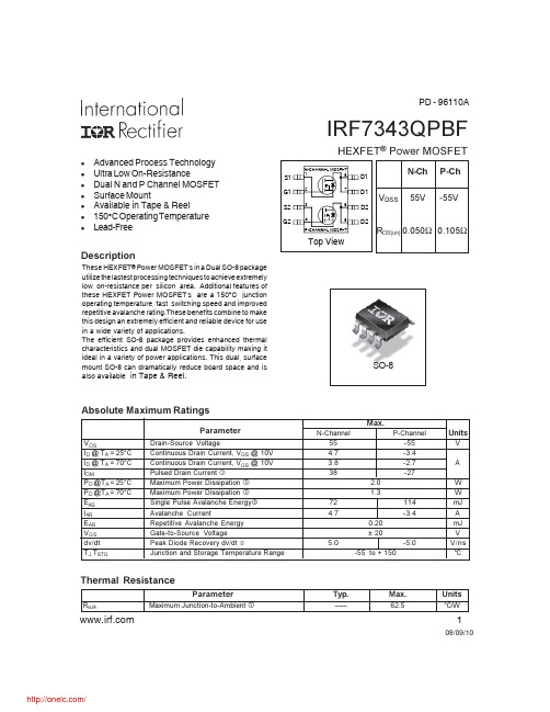
IRF7343QPBF
HEXFET® Power MOSFET
N-CHANNEL MOSFET
S1
1
8
D1
N-Ch P-Ch
G1
2
S2
3
7
D1
VDSS 55V -55V
6
D2
G2
4
5
D2
P-CHANNEL MOSFET
RDS(on) 0.050Ω 0.105Ω
Top View
SO-8
Absolute Maximum Ratings
12V 10V
8.0V 46..50VV 4.0V 3.5V
BOTTOM 3.0V
10
3.0V
20µs PULSE WIDTH
TJ= 25 °C 1
0.1
1
10
100
VDS , Drain-to-Source Voltage (V)
Fig 1. Typical Output Characteristics
Description
These HEXFET® Power MOSFET's in a Dual SO-8 package utilize the lastest processing techniques to achieve extremely low on-resistance per silicon area. Additional features of these HEXFET Power MOSFET's are a 150°C junction operating temperature, fast switching speed and improved repetitive avalanche rating.These benefits combine to make this design an extremely efficient and reliable device for use in a wide variety of applications. The efficient SO-8 package provides enhanced thermal characteristics and dual MOSFET die capability making it ideal in a variety of power applications. This dual, surface mount SO-8 can dramatically reduce board space and is also available in Tape & Reel.
NEC N3303 说明书

开关机键,在待机状 态下,短按该键可直 接进入主菜单
充电器/数据线插槽
Ⅶ
摄像头 拍摄键
电池释放点 音量键
扬声器 自拍镜 电池释放点
手机后盖
触屏笔
挂绳孔,取下手机后盖,将饰物 挂绳穿入孔中,盖上手机后盖, 将饰物固定
按键功能 按键名称 开 /关机键 发送键 音量键
锁屏幕键 拍摄键
按键功能 在待机状态下,短按该键可直接进入主菜单。 拨打 /接听电话;在待机状态下(触摸屏未锁定)进入已拨电话列表。 在待机状态下(触摸屏未锁定)或在通话过程中,按音量键可调节听筒音量; 在主菜单中,按音量键可上、下选择菜单图标; 在照相机拍摄预览窗口,按音量键可用于调节焦距; 当接听模式设置为任意键接听,有来电呼入时,按音量键可应答来电; 在游戏界面,按音量键可关闭背景音乐。 在待机状态下,向下推动锁屏幕键,锁定屏幕; 在屏幕锁定状态下,向下推动锁屏幕键,打开屏幕锁。 在待机状态下进入拍摄预览模式,拍摄预览模式下摄像或拍照。
为了对本产品进行不断改进,本机型及其附件的规格可 能会有部分或全部改变,恕不另行通知。
Ⅴ
使用之前的准备
蜂窝电话系统结构 每次使用手机时,会涉及到几个不同组织:
网络服务商
网络
WAP 服务提供商
NEC手机制造商
提供SIM卡和收费的服务商
信号的传输者
提供因特网服务
您的手机支持本手册中所介绍的所有功能。然而,为了使用这些功能,您必须有支持这些功能的SIM卡(由网络服 务提供商提供)。即使您有功能齐全的 SIM卡,若传输网络不支持,则手机仍无法使用这些功能。 用户手册指南 以下为本操作手册中所使用的图标。
医院安全守则 在禁止使用手机的地方,请关闭手机。使用手机时请
PT3321N;PT3322N;PT3324N;PT3327N;PT3321C;中文规格书,Datasheet资料

pins 2 & 4 connected
Between +Vo and –Vo
Input-output/input-case Input-output Input-output Over Vin range
Vo ≥ 9V Vo ≤ 5V
Per Bellcore TR-332 50% stress, Ta =40°C, ground benign
/
For technical support and more information, see inside back cover or visit
PT3320 Series
30-W 48-V Input Isolated DC/DC Converter
PT Series Suffix (PT1234 x )
Case/Pin Configuration
Order Suffix
Package Code *
Vertical Horizontal SMD
N
(EHG)
A
(EHH)
C
(EHJ)
* Previously known as package styles 840 & 850.
Per Mil-Std-883D, method 2002.3, 1mS, half-sine, mounted to a fixture
Per Mil-Std-883D, method 2007.2, 20-2000Hz, soldered in board
—
Materials meet UL 94V-0
(2) The Remote On/Off input has an internal pull-up. If it is left open circuit the module will operate when input power is applied. A low-leakage (<100nA) MOSFET is recommended to control this input. The open-circuit voltage is less than 10V. See application notes for interface considerations.
PT4401N;PT4403N;PT4401A;PT4403A;中文规格书,Datasheet资料

For technical support and more information, see inside back cover or visit 75-W 48-V Input Isolated DC/DC ConverterFeatures•Up to 75W Output:20A @3.3V , 15A @5V •Input Voltage Range:36V to 75V•Programmable Output Voltage •91% Efficiency (PT4403)•1500 VDC Isolation •On/Off Control•Over-Current ProtectionSLTS160B(Revised 7/19/2002)•Differential Remote Sense•Output Over-Voltage Protection •Over-T emperature Shutdown •Undervoltage Lockout•Low Profile Package (12mm)•Compact PCB Layout:(Horizontal Config. 1.45in × 2.6in, V ertical Config. < 1 in 2)•Solderable Copper Case •Agency Approvals PendingFor technical support and more information, see inside back cover or visit PT4401VID4=1VID4=0VID3VID2VID1VID0VoutVout1111N/D * 1.30V 1110 2.10V 1.35V 1101 2.20V 1.40V 1100 2.30V 1.45V 1011 2.40V 1.50V 1010 2.50V 1.55V 1001 2.60V 1.60V 1000 2.70V 1.65V 0111 2.80V 1.70V 0110 2.90V 1.75V 0101 3.00V 1.80V 0100 3.10V 1.85V 0011 3.20V 1.90V 0010 3.30V 1.95V 0001 3.40V 2.00V 03.50V2.05VLogic 0=Pin 12 potential; (–)Remote Sense Logic 1=Open circuit (no pull-up resistors)Notes (i)See SOA curves or consult factory for appropriate derating(ii)The case pins on the through-hole package types (suffixes N &A) must be soldered. For more information see the applicable package outline drawing.Output Voltage Programming InformationPin Descriptions+Vin: The positive input for the module with respect to –V in . When powering the module from a –48V telecom central office supply, this input is connected to the primary system ground.–Vin: The negative input supply for the module, and the 0VDC reference for the Remote On/Off input. When powering the module from a +48V supply, this input is connected to the 48V(Return).Remote On/Off: A positive logic input that is referenced to –V in . Pulling this input down to –V in potential disables the module’s output. If this input is left open-circuit, the module will produce an output whenever a valid input source is applied.VID0 – VID4: Selects the set-point output voltage of the converter according to the applicable program code.VID0 – VID4 must either be connected to (–)Remote Sense or left open circuit. Note: For the PT4402 & PT4403,VID 4 is internally disabled and may be left open circuit.+Vo: The positive power output with respect to -V o , which is DC isolated from the input supply pins. If a negative output voltage is desired, +V o should be connected to the secondary circuit common and the output taken from –V o .–Vo: The negative power output with respect to +V o ,which is DC isolated from the input supply pins. This output is normally connected to the secondary circuit common when a positive output voltage is desired.+Remote Sense: Provides the converter with remote sense capability to regulate the set-point voltage directly at the load. When used with –Remote Sense, the regulation circuitry will compensate for voltage drop between the converter and the load. The pin may be left open circuit,but connecting it to +V o will improve load regulation.–Remote Sense: This is the logic ‘0’ reference for the inputs VID0 – VID4, and provides the converter with remote sense capability when used in conjunction with +Remote Sense. For optimum output voltage accuracy this pin should always be connected to –V o .PT4402VID4= × †VoutN/D *1.05V 1.10V 1.15V 1.20V 1.25V 1.30V 1.35V 1.40V 1.45V 1.50V 1.55V 1.60V 1.65V 1.70V 1.75VPT4403VID4= × †VoutN/D *3.40V 3.56V 3.72V 3.88V 4.05V 4.21V 4.37V 4.53V 4.69V 4.86V 5.02V 5.18V 5.34V 5.50V 5.67V*N/D = Output voltage is not defined†VID 4 (pin 11) of PT4402 & PT4403 is don’t care (×).Note:During operation, changes to the program code should be limited to 15% of V o so as to avoid activating the output OV protection.For technical support and more information, see inside back cover or visit Note A: All data listed in the above graphs has been developed from actual products tested at 25°C. This data is considered typical data for the DC-DC Converter.Note B: SOA curves represent operating conditions at which internal components are at or below manufacturer’s maximum rated operating temperature.Notes:(1)If (–)Remote Sense is not used, pin 12 must be connected to pin 13 for optimum output voltage accuracy.(2)The Remote On/Off input has an internal pull-up. If it is left open-circuit the module will operate when input power is applied. A discrete MOSFET orbipoloar transistor is recommended to control this input. The open-circuit voltage is typically 5V . See application notes for interface considerations.For technical support and more information, see inside back cover or visit Note A: All data listed in the above graphs has been developed from actual products tested at 25°C. This data is considered typical data for the DC-DC Converter.Note B: SOA curves represent operating conditions at which internal components are at or below manufacturer’s maximum rated operating temperature.Notes:(1)If (–)Remote Sense is not used, pin 12 must be connected to pin 13 for optimum output voltage accuracy.(2)The Remote On/Off input has an internal pull-up. If it is left open-circuit the module will operate when input power is applied. A discrete MOSFET orbipoloar transistor is recommended to control this input. The open-circuit voltage is typically 5V . See application notes for interface considerations.For technical support and more information, see inside back cover or visit Note A: All data listed in the above graphs has been developed from actual products tested at 25°C. This data is considered typical data for the DC-DC Converter.Note B: SOA curves represent operating conditions at which internal components are at or below manufacturer’s maximum rated operating temperature.Notes:(1)If (–)Remote Sense is not used, pin 12 must be connected to pin 13 for optimum output voltage accuracy.(2)The Remote On/Off input has an internal pull-up. If it is left open-circuit the module will operate when input power is applied. A discrete MOSFET orbipoloar transistor is recommended to control this input. The open-circuit voltage is typically 5V . See application notes for interface considerations.Operating Features and System Considerations for the PT4400 Series of Isolated DC/DC ConvertersOver-Current ProtectionT o protect against load faults, the PT4400 series incor-porates output over-current protection. Applying a load that exceeds the converter’s over-current threshold (see applicable specification) will cause the regulated output to momentarily fold back and shut down. Following shutdown the module will periodically attempt to auto-matically recover by initiating a soft-start power-up. This is often described as a “hiccup” mode of operation, whereby the module continues in the cycle of succesive shutdown and power up until the load fault is removed. Once the fault is removed, the converter then automatically recovers and returns to normal operation.Output Over-Voltage ProtectionThe PT4400 DC/DC converter series incorporates pro-tection circuitry that continually senses for an output overvoltage (OV) condition. The OV threshold auto-matically tracks the VID output voltage program setting to a level that is 25% higher than that programmed at the control pins, VID0 through VID4. If the converter output voltage exceeds this OV threshold, the converter is immediately shut down and remains in a latched-off state. In order to resume normal operation the converter must be actively reset. This can only be done by momen-tarily removing the input power to the converter. For failsafe operation and redundancy, the OV protection uses circuitry that is independent of the converter’s internal feedback loop.Over-Temperature ProtectionOver-temperature protection is provided by an internal temperature sensor, which closely monitors the tempera-ture of the converter’s metal case. If the case temperature exceeds a nominal 115°C, the converter will shut down. The converter will then automatically restart when the sensed temperature drops back to approximately 105°C. When operated outside its recommended thermal derating envelope (see data sheet SOA curves), the converter will typcially cycle on and off at intervals from a few seconds to one or two minutes. This is to ensure that the internal components are not permanently damaged from exces-sive thermal stress.Under-Voltage LockoutThe Under-Voltage Lock-Out (UVLO) is designed to prevent the operation of the converter until the input voltage is close to the minimum input voltage. The converter is held off when the input voltage is below the UVLO threshold, and turns on when the input voltage rises above the threshold. This prevents high start-up current during normal power-up of the converter, and minimizes the current drain from the input source during low input voltage conditions. The converter will meet full specifications when the minimum specified input voltage is reached. The UVLO circuitry also overrides the operation of the Remote On/Off control. Only when the input voltage is above the UVLO threshold will the Remote On/Off control be functional.Primary-Secondary IsolationThe PT4400 DC/DC converter series incorporates elec-trical isolation between the input terminals (primary) and the output terminals (secondary). All converters are production tested to a withstand voltage of 1500VDC. This specification complies with UL60950 and EN60950 and the requirements for operational isolation. This allows the converter to be configured for either a positive or negative input voltage source. The data sheet ‘Pin De-scriptions’ section provides guidance as to the correct reference that must be used for the external control signals. Fuse RecommendationsIf desired, an input fuse may be added to protect against the application of a reverse input voltage.Thermal ConsiderationsAirflow may be necessary to ensure that the module can supply the desired load current in environments with elevated ambient temperatures. The required airflow rate may be determined from the Safe Operating Area (SOA) thermal derating chart (see converter specifica-tions). The recommended direction for airflow is into, or perpendicular to, the longest side of the module’smetal case. See Figure 1.into (perpendicular to) the longest side.Figure 1For technical support and more information, see inside back cover or visit Using the Remote On/Off Function on the PT4400 Series of Isolated DC/DC ConvertersFor applications requiring output voltage On/Off control, the PT4400 DC/DC converter series incorporates a “Re-mote On/Off” control (pin 1). This feature can be used toswitch the module off without removing the applied input source voltage.The converter functions normally with Pin 1 open-circuit, providing a regulated output voltage when a valid source voltage is applied to +V in (pins 4, 5), with respect to-V in (pins 2, 3). When a low-level 1 ground signal is applied to pin 1, the converter output will be turned off. Figure 1 is an application schematic, which shows the typical use of the Remote On/Off function. Note the dis-crete transistor (Q1). The Remote On/Off pin has its own internal pull-up, allowing it to be controlled with an open-collector or open-drain device (See notes 2 & 3).T able 1 gives the threshold requirements.When placed in the “Off” state, the standby current drawn from the input source is typically reduced to less than 1mA.Table 1; Pin 1 Remote On/Off Control Requirements 1Parameter Min Typ MaxEnable (V IH) 4.5V——Disable (V IL)——0.8VV o/c [Open-Circuit] 5.0VI in [pin 1 at –V in]——–0.5mANotes:1.The Remote On/Off control uses –V in (pins 2, 3) as itsground reference. All voltages are with respect to –V in. e an open-collector device (preferably a discretetransistor) for the Remote On/Off input. A pull-upresistor is not necessary. T o disable the output voltage, the control pin should be pulled low to less than +0.8V.3.The Remote On/Off pin may be controlled with devices thathave a totem-pole output. This is provided the output high-level voltage (V OH) meets the module’s minimum V IH specified in T able 1. Do not apply more than +20V.If a TTL gate is used, a pull-up resistor may be required to the logic supply voltage.4.The PT4400 converters incorporate an “Under-VoltageLockout” (UVLO). The UVLO keeps the converter off until the input voltage is close to the minimumspecified operating voltage. This is regardless of the state of the Remote On/Off control. Table 2 gives the UVLO input voltage thresholds.Figure 1Turn-On Time: In the circuit of Figure 1, turning Q1 on applies a low-voltage to pin 1 and disables the converter output. Correspondingly, turning Q1 off allows pin 1to be pulled high by an internal pull-up resistor. The con-verter produces a regulated output voltage within 50ms. Figure 2 shows the output response of a PT4401 following the turn-off of Q1. The turn off of Q1 corresponds to the drop in Q1 Vgs. Although the rise-time of the output voltage is short (<5ms), the indicated delay time will vary depending upon the input voltage and the module’s internal timing. The output voltage of the PT4401 was set to 3.3V by connecting VID0 (pin 7), VID2 (pin 9), and VID3 (pin 10) to the (–)Remote Sense (pin 12). The waveforms were measured with 48VDC input voltage, and a 10A resistive load.Figure 2–Table 2; UVLO Thresholds 4Series V in Range UVLO ThresholdPT440036 – 75V32V ±2VQ1 Vgs (10V/Div)For technical support and more information, see inside back cover or visit Pin-Coded Output Voltage Adjustment on thePT4400 Programmable DC/DC ConvertersThe PT4400 series of isloated DC/DC converters have a programmable output voltage. In each case the desired output voltage must be selected from one of a number of discrete voltages using the voltage programming control pins. Depending on each model’s resolution and adjust-ment range, there are up to five control pins. They are identified VID0–VID4 (pins 7–11) respectively. By selectively strapping these control pins to (–)Remote Sense (pin 12), the output voltage can be programmed in incremental steps over the defined output voltage range. The program code and output voltage range of the PT4401 is also compatible with the “Voltage ID” code defined in the Intel® VRM 8.2 specification. Refer to Figure 1 for the connection schematic, and the product specification sheet for each model’s applicable program code.Notes:1.The programming convention is as follows:-Logic 0:Connect to pin 12 (–Remote Sense).Logic 1:Open circuit/open drain (See notes 2, & 4) 2.Do not connect pull-up resistors to the voltageprogramming pins.3.T o minimize output voltage error, always use pin 12(-Remote Sense) as the logic “0” reference. While -Vout (pins 13-16) can also be used for programming, doing so will degrade the voltage selection accuracy and loadregulation of the product.4.When VID0–VID4 are all open circuit (logic 1), theoutput voltage is undefined. In this state the outputvoltage of the converter cannot be guaranteed, and can vary with output load and input voltage.Figure 15.On all models other than the PT4401, the contol inputVID4 (pin 11) is internally disabled and not functional.6.If active devices are used to ground the voltage controlpins, low-level open drain MOSFET devices should beused over bipolar transistors. The inherent V ce(sat) inbipolar devices introduces errors in the device’s internalvoltage control circuit. Discrete transistors such as theBSS138 or IRLML2402 are examples of appropriatedevices.Active Voltage Programming:Special precautions should be taken when making changes to the voltage progam code while the output is active. This activity induces a transient, which may activate the module’s output over-voltage (OV) protection. Once triggered the OV protection circuit latches the output off, and requires the momentary removal of input power to reset the module. OV protection trips can be avoided by limiting the output voltage adjustment to no more than a 15% change from the initial voltage. Large transi-tions are best made with a series of incremental changes, allowing 100µs settling time between each program state. When using active devices to program the output voltage, their state should be asserted prior to input power being applied. An alternative is to pull pin 1 (Remote On/Off) to -V in (pins 2, 3) during the application of power, assert the required program code, and then release pin 1. The module will than initiate a soft-start power-up to the desired program voltage.–For technical support and more information, see inside back cover or visit PACKAGAddendum-Page 1PACKAGING INFORMATIONOrderable DeviceStatus(1)Package Type PackageDrawing Pins Package QtyEco Plan(2)Lead/Ball Finish MSL PeaPT4401N NRND SIP MODULEENM 218TBD Call TI Level-1-215C PT4403NOBSOLETE SIP MODULEENM21TBDCall TICall TI(1)The marketing status values are defined as follows:ACTIVE: Product device recommended for new designs.LIFEBUY: TI has announced that the device will be discontinued, and a lifetime-buy period is in effect.NRND: Not recommended for new designs. Device is in production to support existing customers, but TI does not recommend using this part in a new PREVIEW: Device has been announced but is not in production. Samples may or may not be available.OBSOLETE: TI has discontinued the production of the device.(2)Eco Plan - The planned eco-friendly classification: Pb-Free (RoHS), Pb-Free (RoHS Exempt), or Green (RoHS & no Sb/Br) - please check http://www.t information and additional product content details.TBD: The Pb-Free/Green conversion plan has not been defined.Pb-Free (RoHS): TI's terms "Lead-Free" or "Pb-Free" mean semiconductor products that are compatible with the current RoHS requirements for all lead not exceed 0.1% by weight in homogeneous materials. Where designed to be soldered at high temperatures, TI Pb-Free products are suitable fo Pb-Free (RoHS Exempt): This component has a RoHS exemption for either 1) lead-based flip-chip solder bumps used between the die and package, the die and leadframe. The component is otherwise considered Pb-Free (RoHS compatible) as defined above.Green (RoHS & no Sb/Br): TI defines "Green" to mean Pb-Free (RoHS compatible), and free of Bromine (Br) and Antimony (Sb) based flame retard in homogeneous material)(3)MSL, Peak Temp. -- The Moisture Sensitivity Level rating according to the JEDEC industry standard classifications, and peak solder temperature.Important Information and Disclaimer:The information provided on this page represents TI's knowledge and belief as of the date that it is provided. TI provided by third parties, and makes no representation or warranty as to the accuracy of such information. Efforts are underway to better integrate inf continues to take reasonable steps to provide representative and accurate information but may not have conducted destructive testing or chemical an TI and TI suppliers consider certain information to be proprietary, and thus CAS numbers and other limited information may not be available for releasIn no event shall TI's liability arising out of such information exceed the total purchase price of the TI part(s) at issue in this document sold by TI to Cu/IMPORTANT NOTICETexas Instruments Incorporated and its subsidiaries(TI)reserve the right to make corrections,enhancements,improvements and other changes to its semiconductor products and services per JESD46,latest issue,and to discontinue any product or service per JESD48,latest issue.Buyers should obtain the latest relevant information before placing orders and should verify that such information is current and complete.All semiconductor products(also referred to herein as“components”)are sold subject to TI’s terms and conditions of sale supplied at the time of order acknowledgment.TI warrants performance of its components to the specifications applicable at the time of sale,in accordance with the warranty in TI’s terms and conditions of sale of semiconductor products.Testing and other quality control techniques are used to the extent TI deems necessary to support this warranty.Except where mandated by applicable law,testing of all parameters of each component is not necessarily performed.TI assumes no liability for applications assistance or the design of Buyers’products.Buyers are responsible for their products and applications using TI components.To minimize the risks associated with Buyers’products and applications,Buyers should provide adequate design and operating safeguards.TI does not warrant or represent that any license,either express or implied,is granted under any patent right,copyright,mask work right,or other intellectual property right relating to any combination,machine,or process in which TI components or services are rmation published by TI regarding third-party products or services does not constitute a license to use such products or services or a warranty or endorsement e of such information may require a license from a third party under the patents or other intellectual property of the third party,or a license from TI under the patents or other intellectual property of TI.Reproduction of significant portions of TI information in TI data books or data sheets is permissible only if reproduction is without alteration and is accompanied by all associated warranties,conditions,limitations,and notices.TI is not responsible or liable for such altered rmation of third parties may be subject to additional restrictions.Resale of TI components or services with statements different from or beyond the parameters stated by TI for that component or service voids all express and any implied warranties for the associated TI component or service and is an unfair and deceptive business practice. TI is not responsible or liable for any such statements.Buyer acknowledges and agrees that it is solely responsible for compliance with all legal,regulatory and safety-related requirements concerning its products,and any use of TI components in its applications,notwithstanding any applications-related information or support that may be provided by TI.Buyer represents and agrees that it has all the necessary expertise to create and implement safeguards which anticipate dangerous consequences of failures,monitor failures and their consequences,lessen the likelihood of failures that might cause harm and take appropriate remedial actions.Buyer will fully indemnify TI and its representatives against any damages arising out of the use of any TI components in safety-critical applications.In some cases,TI components may be promoted specifically to facilitate safety-related applications.With such components,TI’s goal is to help enable customers to design and create their own end-product solutions that meet applicable functional safety standards and requirements.Nonetheless,such components are subject to these terms.No TI components are authorized for use in FDA Class III(or similar life-critical medical equipment)unless authorized officers of the parties have executed a special agreement specifically governing such use.Only those TI components which TI has specifically designated as military grade or“enhanced plastic”are designed and intended for use in military/aerospace applications or environments.Buyer acknowledges and agrees that any military or aerospace use of TI components which have not been so designated is solely at the Buyer's risk,and that Buyer is solely responsible for compliance with all legal and regulatory requirements in connection with such use.TI has specifically designated certain components which meet ISO/TS16949requirements,mainly for automotive ponents which have not been so designated are neither designed nor intended for automotive use;and TI will not be responsible for any failure of such components to meet such requirements.Products ApplicationsAudio /audio Automotive and Transportation /automotiveAmplifiers Communications and Telecom /communicationsData Converters Computers and Peripherals /computersDLP®Products Consumer Electronics /consumer-appsDSP Energy and Lighting /energyClocks and Timers /clocks Industrial /industrialInterface Medical /medicalLogic Security /securityPower Mgmt Space,Avionics and Defense /space-avionics-defense Microcontrollers Video and Imaging /videoRFID OMAP Applications Processors /omap TI E2E Community Wireless Connectivity /wirelessconnectivityMailing Address:Texas Instruments,Post Office Box655303,Dallas,Texas75265Copyright©2012,Texas Instruments Incorporated分销商库存信息:TIPT4401N PT4403N PT4401A PT4403A。
- 1、下载文档前请自行甄别文档内容的完整性,平台不提供额外的编辑、内容补充、找答案等附加服务。
- 2、"仅部分预览"的文档,不可在线预览部分如存在完整性等问题,可反馈申请退款(可完整预览的文档不适用该条件!)。
- 3、如文档侵犯您的权益,请联系客服反馈,我们会尽快为您处理(人工客服工作时间:9:00-18:30)。
Technical Data Sheet 5mm Phototransistor T-1PT333-3BFeatures․Fast response time ․High photo sensitivity ․Pb free ․This product itself will remain within RoHS compliant version.Descriptions․PT333-3B is a high speed and high sensitive NPN silicon NPN epitaxial planar phototransistor molded in a standard 5 mm package. Due to is black epoxy the device is sensitive to visible and near Infrared radiation.Applications․Infrared applied system ․Camera ․Cockroach catcherDevice Selection Guide LED Part No.PT333-3BChip MaterialSiliconLens ColorBlackEverlight Electronics Co., Ltd. Device No:CDPT-033-010http:\\ Prepared date:2006/01/10Rev 1Page: 1 of 7Prepared by:Fealty zhu/PT333-3BPackage DimensionsNotes: 1.All dimensions are in millimeters 2.Tolerances unless dimensions ±0.25mmAbsolute Maximum Ratings (Ta=25℃)Parameter Collector-Emitter Voltage Emitter-Collector-Voltage Collector Current Operating Temperature Storage Temperature Lead Soldering Temperature(*1) Power Dissipation at (or below) 25℃ Free Air Temperature Symbol VCEO VECO IC Topr Tstg Tsol Pc Rating 30 5 20 -25 ~ +85℃ -40 ~ +85℃ 260 75 Units V V mA ℃ ℃ ℃ mWNotes: *1:Soldering time≦5 seconds.Everlight Electronics Co., Ltd. Device No:CDPT-033-010 http:\\ Prepared date:2006/01/10 Rev 1 Page: 2 of 7Prepared by:Fealty zhu/PT333-3BElectro-Optical Characteristics (Ta=25℃)Parameter Collector – Emitter Breakdown Voltage Emitter-Collector Breakdown Voltage Collector-Emitter Saturation Voltage Rise Time Fall Time Collector Dark Current On State Collector Current Wavelength of Peak Sensitivity Rang of Spectral Bandwidth Symbol BVCEO Condition IC=100μA Ee=0mW/cm2 Min. 30 5 --------0.7 ----Typ. ------15 15 --3.0 940 840-1100 Max. ----0.4 ----100 ------Units V V V μS nA mA nm nmIE=100μA BVECO Ee=0mW/cm2 IC=2mA VCE)(sat) Ee=1mW/cm2 tr tf ICEO IC(on) λp λ0.5 VCE=5V IC=1mA RL=1000Ω Ee=0mW/cm2 VCE=20V Ee=1mW/cm2 VCE=5V -----RankingsParameter G H J K L Ic(ON) Symbol Min 0.70 1.14 1.77 2.67 4.18 Max 1.90 2.60 3.61 5.07 7.07 mA Unit Test Condition VcE=5V Ee=1mW/cm²Everlight Electronics Co., Ltd. Device No:CDPT-033-010http:\\ Prepared date:2006/01/10Rev 1Page: 3 of 7Prepared by:Fealty zhu/PT333-3BTypical Electro-Optical Characteristics CurvesFig.1Collector Power Dissipation vs. Ambient Temperature 160140 120 100 80 Ambient Temperature 60 40 20 0 0 10 20 30 40 50 60 702Fig.2 Spectral Sensitivity1.0 Ta=25 C 0.8 0.6 0.4 0.2 0O600 700 800 900 1000 1100 1200Fig.3 Relative Collector Current vs. Ambient TemperatureFig.4 Collector Current vs. Irradiance100 80 60100 C 10 140 20 00.1 0.01 0.5-250255075 85 10011.523Everlight Electronics Co., Ltd. Device No:CDPT-033-010http:\\ Prepared date:2006/01/10Rev 1Page: 4 of 7Prepared by:Fealty zhu/PT333-3BTypical Electro-Optical Characteristics CurvesFig.5 Collector Dark Current vs. Ambient Temperature Fig.6 Collector Current vs. Collector-Emitter Voltage1014 1210 1010 8 6 4 210 10 0 25 50 75 1000 01234Everlight Electronics Co., Ltd. Device No:CDPT-033-010http:\\ Prepared date:2006/01/10Rev 1Page: 5 of 7Prepared by:Fealty zhu/PT333-3BReliability Test Item And ConditionThe reliability of products shall be satisfied with items listed below. Confidence level:90% LTPD:10% NO. Item Test Conditions Test Hours/ Sample Cycles Sizes 10secs 22pcs 22pcs IC(ON)≦L×0.8 22pcs L:the initial test 0/1 value 0/1 0/1 0/1 0/1 Failure Judgement Criteria Ac/Re1 Solder HeatTEMP.:260℃±5℃0/1 0/12 Temperature Cycle H : +100℃ L : -40℃ 3 Thermal Shock H :+100℃ L :-10℃ 4 High Temperature Storage 5 Low Temperature Storage15mins 300Cycles 5mins 15mins 5mins 300Cycles 10secs 5mins 1000hrs 1000hrs 1000hrs 1000hrsTEMP.:+100℃ TEMP.:-40℃22pcs 22pcs 22pcs 22pcs6 DC Operating Life VCE=5V 7 High Temperature/ 85℃ / 85% R.H High HumidityEverlight Electronics Co., Ltd. Device No:CDPT-033-010http:\\ Prepared date:2006/01/10Rev 1Page: 6 of 7Prepared by:Fealty zhu/PT333-3BPacking Quantity Specification1.500PCS/1Bag,5Bags/1Box 2.10Boxes/1CartonLabel Form SpecificationPT333-3BCPN: Customer’s Production Number P/N : Production Number QTY: Packing Quantity CAT: Ranks HUE: Peak Wavelength REF: Reference LOT No: Lot NumberNotes1. Above specification may be changed without notice. EVERLIGHT will reserve authority on material change for above specification. 2. When using this product, please observe the absolute maximum ratings and the instructions for using outlined in these specification sheets. EVERLIGHT assumes no responsibility for any damage resulting from use of the product which does not comply with the absolute maximum ratings and the instructions included in these specification sheets. 3. These specification sheets include materials protected under copyright of EVERLIGHT corporation. Please don’t reproduce or cause anyone to reproduce them without EVERLIGHT’s consent.EVERLIGHT ELECTRONICS CO., LTD. Office: No 25, Lane 76, Sec 3, Chung Yang Rd, Tucheng, Taipei 236, Taiwan, R.O.C Tel: 886-2-2267-2000, 2267-9936 Fax: 886-2267-6244, 2267-6189, 2267-6306 http:\\Everlight Electronics Co., Ltd. Device No:CDPT-033-010http:\\ Prepared date:2006/01/10Rev 1Page: 7 of 7Prepared by:Fealty zhu/分销商库存信息:EVERLIGHT PT333-3B。