311SM4-H58;中文规格书,Datasheet资料
LP311中文资料
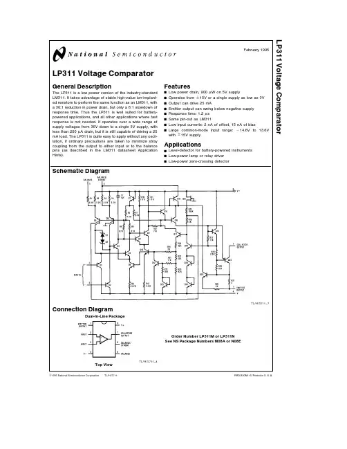
TL H 5711LP311Voltage ComparatorFebruary 1995LP311Voltage ComparatorGeneral DescriptionThe LP311is a low power version of the industry-standard LM311 It takes advantage of stable high-value ion-implant-ed resistors to perform the same function as an LM311 with a 30 1reduction in power drain but only a 6 1slowdown of response time Thus the LP311is well suited for battery-powered applications and all other applications where fast response is not needed It operates over a wide range of supply voltages from 36V down to a single 3V supply with less than 200m A drain but it is still capable of driving a 25mA load The LP311is quite easy to apply without any oscil-lation if ordinary precautions are taken to minimize stray coupling from the output to either input or to the balance pins (as described in the LM311datasheet Application Hints)FeaturesY Low power drain 900m W on 5V supplyY Operates from g 15V or a single supply as low as 3V Y Output can drive 25mAY Emitter output can swing below negative supply Y Response time 1 2m s Y Same pin-out as LM311Y Low input currents 2nA of offset 15nA of biasYLarge common-mode input range b 14 6V to 13 6V with g 15V supplyApplicationsY Level-detector for battery-powered instruments Y Low-power lamp or relay driver YLow-power zero-crossing detectorSchematic DiagramTL H 5711–7Connection DiagramDual-In-Line PackageTL H 5711–4Top ViewOrder Number LP311M or LP311N See NS Package Numbers M08A or N08EC 1995National Semiconductor CorporationRRD-B30M115 Printed in U S AAbsolute Maximum RatingsIf Military Aerospace specified devices are required please contact the National Semiconductor Sales Office Distributors for availability and specifications Total Supply Voltage(V8–4)36V Collector Output to Negative Supply Voltage(V7–4)40V Collector Output to Emitter Output40V Emitter Output to Negative Supply Voltage(V1–4)g30V Differential Input Voltage g30V Input Voltage(Note1)g15V Power Dissipation(Note2)500mW Output Short Circuit Duration10sec Operating Temperature Range0 C to70 C Storage Temperature Range b65 C to150 C Lead Temperature(Soldering 10seconds)260 CElectrical CharacteristicsThese specifications apply for V S e g15V and0 C s T A s70 C unless otherwise specifiedParameter Conditions Min Typ Max Units Input Offset Voltage(Notes3 4)T A e25 C R S s100k2 07 5mVInput Offset Current(Notes3 4)T A e25 C2 025nA Input Bias Current(Note3)T A e25 C15100nA Voltage Gain T A e25 C R L e5k40200V mV Response Time(Note5)T A e25 C1 2m sSaturation Voltage(Note6)V IN s b10mV I OUT e25mA0 41 5VT A e25 CStrobe Current(Note7)T A e25 C100200300m AOutput Leakage Current V IN t10mV V OUT e35V0 2100nAT A e25 CInput Offset Voltage(Notes3 4)R S s100k10mV Input Offset Current(Notes3 4)35nA Input Bias Current(Note3)150nA Input Voltage Range V b a0 5a13 7 b14 7V a b1 5VSaturation Voltage(Note6)V a t4 5V V b e0V0 10 4VV IN s b10mV I SINK s1 6mAPositive Supply Current T A e25 C Output on150300m A Negative Supply Current T A e25 C80180m A Minimum Operating Voltage T A e25 C3 03 5V Note1 This rating applies for g15V supplies The positive input voltage limit is30V above the negative supply The negative input voltage limit is equal to the negative supply voltage or30V below the positive supply whichever is lessNote2 The maximum junction temperature of the LP311is85 C For operating at elevated temperatures devices in the dual-in-line package must be derated based on a thermal resistance of160 C W junction to ambientNote3 The offset voltage offset current and bias current specifications apply for any supply voltage from a single4V supply up to g15V suppliesNote4 The offset voltages and offset currents given are the maximum values required to drive the output within a volt of either supply with1mA load Thus these parameters define an error band and take into account the worst-case effects of voltage gain and input impedanceNote5 The response time specified is for a100mV input step with5mV overdriveNote6 Saturation voltage specification applies to collector-emitter voltage(V7-1)for V COLLECTOR s(V a b3V)Note7 This specification gives the range of current which must be drawn from the strobe pin to ensure the output is properly disabled Do not short the strobe pin to ground It should be current driven 100m A to300m A2Typical Performance CharacteristicsInput Characteristics Input Bias Current Input Offset CurrentCommon Mode Limits Transfer Function Output Saturation Voltage (Collector Output)Response Time for Various Input Overdrives Response Time for VariousInput OverdrivesOutput Saturation Voltage(Emitter Output)Response Time for Various Input Overdrives Response Time for VariousInput OverdrivesOutput LimitingCharacteristicsTL H 5711–5 3Typical Performance Characteristics(Continued)Supply CurrentSupply CurrentLeakage CurrentsTL H 5711–6Applications InformationFor applications information and typical applications refer to the LM311datasheetAuxiliary CircuitsStrobingTL H 5711–1Note Do not ground strobe pinOffset BalancingTL H 5711–2Test CircuitsTest Circuit 1(Collector Output)TL H 5711–8Test Circuit 2(Emitter Output)TL H 5711–9Test Circuit 3(Collector Output)TL H 5711–10Test Circuit 4(Emitter Output)TL H 5711–114Physical Dimensions inches(millimeters)Order Number LP311MNS Package Number M08A5L P 311V o l t a g e C o m p a r a t o rPhysical Dimensions inches (millimeters)(Continued)Molded Dual-In-Line Package (N)Order Number LP311N NS Package Number N08ELIFE SUPPORT POLICYNATIONAL’S PRODUCTS ARE NOT AUTHORIZED FOR USE AS CRITICAL COMPONENTS IN LIFE SUPPORT DEVICES OR SYSTEMS WITHOUT THE EXPRESS WRITTEN APPROVAL OF THE PRESIDENT OF NATIONAL SEMICONDUCTOR CORPORATION As used herein 1 Life support devices or systems are devices or 2 A critical component is any component of a life systems which (a)are intended for surgical implant support device or system whose failure to perform can into the body or (b)support or sustain life and whose be reasonably expected to cause the failure of the life failure to perform when properly used in accordance support device or system or to affect its safety or with instructions for use provided in the labeling can effectivenessbe reasonably expected to result in a significant injury to the userNational Semiconductor National Semiconductor National Semiconductor National Semiconductor CorporationEuropeHong Kong LtdJapan Ltd1111West Bardin RoadFax (a 49)0-180-530858613th Floor Straight Block Tel 81-043-299-2309。
Tenda无线路由器说明书

12.1 路由表 ......................................................................64 12.2 静态路由...................................................................65
第2章 产品安装.................................................................... 6
2.1 硬件安装 ....................................................................... 6 2.2 网络应用拓扑 ................................................................ 8
第10章 上网监控 ...................................................................54
10.1 上网监控 ....................................................................54
第7章: DHCP服务器 ...........................................................42
7.1 DHCP服务设置...........................................................42 7.2 DHCP列表与绑定 .......................................................43
SEL311L调试大纲Z004-2005
深圳市华力特电气有限公司企业标准Q/SZFARAD/Z004---2005SEL311L调试大纲2005-08-5发布 2005-08-15实施深圳市华力特电气有限公司Q/SZFARAD/Z004---2005目录1.概述 (3)2.前面板界面 (3)2.1.前面板按钮 (3)2.2.前面板修改定值 (3)2.3.前面板信号灯LED (3)2.3.1.TRIP出口信号 (4)2.3.2.TIME延时跳闸信号 (4)M通讯跳闸信号 (4)2.3.4.重合闸信号 (4)2.3.5.50/51过流/反时限过流跳闸信号 (4)2.3.6.FAULT TYPE故障分相信号 (5)2.3.7.ZONE/LEVEL保护分段指示 (5)2.3.8.87CH 光纤差动通讯通道故障 (5)2.4.信号复归/信号灯测试按钮 (5)3.保护定值和逻辑方程 (5)3.1.光纤差动保护 (5)3.1.1.光纤差动保护定值 (5)3.1.2.光纤差动保护逻辑方程 (7)3.2.PT断线 (7)3.2.1.PT断线定值 (7)3.3.方向元件 (8)3.3.1.方向元件定值 (8)3.4.距离保护 (8)3.4.1.圆特性四段相间距离保护 (8)3.4.2.圆特性四段接地距离保护 (9)3.4.3.四边形特性四段接地距离保护 (9)3.4.4.距离I 段延伸保护 (10)3.4.5.距离保护定值 (10)3.4.6.距离保护逻辑方程 (11)3.5.零序保护及相电流保护 (11)3.5.1.零序和相电流保护定值 (11)3.5.2.零序和相电流保护逻辑方程 (11)3.6.振荡元件 (12)3.6.1.振荡元件定值 (12)3.7.重合闸 (13)3.7.1.重合闸定值 (13)3.7.2.重合闸逻辑方程 (13)3.8.同期 (13)3.8.1.同期定值 (13)3.8.2.同期逻辑方程 (14)SEL-311L调试大纲 1Q/SZFARAD/Z004---2005SEL-311L 调试大纲 2 3.9. 后加速 (14)3.9.1. 后加速定值 (14)3.9.2. 后加速逻辑方程 (14)3.10. 遥控跳/合闸 (14)3.11. 其它逻辑方程 (14)3.12. 自动化信息表 ......................................................................................................................... 15 4. 试验方法 (16)4.1. 试验设备准备 (16)4.2. 继电器上电 (17)4.3. 全局定值整定 (17)4.4. 开入、开出检查 (17)4.5. 遥控 (17)4.6. 交流输入 (17)4.7. PT 断线功能 (18)4.8. 过电流保护 (18)4.9. 检同期重合闸 (18)4.10. 频率元件 (18)4.11. 距离保护 (18)4.12. 光纤差动保护 (20)4.12.1. 单一继电器试验 (20)4.12.2. 双继电器试验 (21)4.12.3. 相 87L 元件测试 ................................................................................................................ 21 5. 故障处理 (25)5.1. 所有前面板信号灯LED 熄灭 (25)5.2. 在继电器显示屏幕上无字符显示 (25)5.3. 继电器不响应串行口来的命令 (25)5.4. 继电器对故障没有响应 ............................................................................................................. 25 5.5. 差动通讯通道故障87CH FAIL 信号灯点亮 . (25)5.6.如果问题仍然存在,联系工厂。
SPU0414HR5H-SB, 规格书,Datasheet 资料
3. TEMPERATURE RANGE
3.1 Operating Temperature Range: -40 C to +100 C 3.2 Storage Temperature Range: -40 C to +100 C
Knowles Acoustics, a division of Knowles Electronics, LLC.
Identification Number Convention S 4 1 5 2 6 3 7
S: Manufacturing Location "S" - Knowles Electronics Suzhou Suzhou, China "No Alpha Character" - Knowles Electronics Itasca, IL USA "E" - Engineering Samples Digits 1-7: Job Identification Number
Date
4-23-2009 10-21-2010
The information contained in this literature is based on our experience to date and is believed to be reliable and it is subject to change without notice. It is intended as a guide for use by persons having technical skill at their own discretion and risk. We do not guarantee favorable results or assume any liability in connection with its use. Dimensions contained herein are for reference purposes only. For specific dimensional requirements consult factory. This publication is not to be taken as a license to operate under, or recommendation to infringe any existing patents. This supersedes and voids all previous literature.
SS311PT;中文规格书,Datasheet资料
SS311PT/SS411PBipolar Hall-effect Digital Position Sensors with Built-in Pull-up ResistorDESCRIPTIONThe SS311PT/SS411P sensors are small, versatile digital Hall-effect devices that are operated by the magnetic field from a permanent magnet or an electromagnet, designed to respond to alternating North and South poles.These bipolar sensors have enhanced sensitivity which allows for the use of smaller, often less expensive magnets. The internal pull-up resistor often eliminates the need for external components, further helping to reduce system cost. These economical bipolar sensors are suited for many simple, high-volume, cost-sensitive, rotary sensing applications.The 2.7 Vdc to 7 Vdc supply voltage range allows this device to be used in low voltage applications. The S311PT’s very small size requires less PCB (printed circuit board) space, allowing it to be used in smaller assemblies.These sensors are available in two package styles: the SS311PT in the subminiature SOT-23 surface mount package and the SS411P in the leaded, flat TO-92-style package.The SS311PT is available on tape and reel (3000 units per reel); the SS411P is available in a bulk package (1000 units per bag).FEATURES• Subminiature, SOT-23 surface mount package (SS311PT)supplied on tape and reel allows for a compact design with automated component placement, helping to reduce manufacturing costs• Small, leaded, flat TO-92 package (SS411P) often allowsfor more space on the PCB• Sensitive, bipolar magnetics respond to alternating Northand South poles, making these products suited for speed sensing and RPM measurement• Built-in pull-up resistor can easily interface with commonelectronic circuits without adding external components, helping to reduce total system cost• RoHS-compliant materials meet Directive 002/95/ECPOTENTIAL APPLICATIONS Transportation:• Speed and RPM (revolutions per minute) sensing • Tachometer, counter pickup • Motor and fan control• Brushless dc motor controlIndustrial and Commercial:• Speed and RPM (revolutions per minute) sensing • Tachometer, counter pickup • Flow-rate sensing• Brushless dc (direct current) motor commutation • Motor and fan control • Robotics controlSS311PT/SS411P2 /sensingTable 1. SS311PT/SS411P Specifications (At 2.7 Vdc to 7 Vdc supply, 4 mA load, T A = -40 ºC to 150 ºC [-40 ºF to 302 ºF]Characteristic Condition Minimum Typical Maximum Unit Supply voltage -40 °C to 150 °C [-40 °F to 302 °F] 2.7 5.0 7.0 Vdc gauss <-140, Vs = 5 V, 25 °C [77°F] – 5.5 –Supply current -40 °C to 150 °C [-40 °F to 302 °F] – – 14mAOutput current – – – 4.0 mA Vsat gauss >140 – – 0.4 VOutput leakage current gauss <-140 – – 10 µAOutput rise timeOutput fall time25 °C [77 °F]– – – – 1.5 1.5 µs Thermal resistance:SS311PT – – 303 –SS411P – – 233 – °C/W Operate -40 °C to 150 °C [-40 °F to 302 °F] -30 55 140 gauss Release -40 °C to 150 °C [-40 °F to 302 °F] -140 -55 30 gauss Differential -40 °C to 150 °C [-40 °F to 302 °F] 40 – – gauss Operating temperature – -40 [-40] – 150 [302] °C [°F] Storage temperature – -40 [-40] – 150 [302] °C [°F]NOTICEBipolar Hall-effect sensors may have an initial output in either the ON or OFF state if powered up with an applied magnetic field in the differential zone (applied magnetic field >Brp and <Bop). Honeywell recommends allowing 10 µs for output voltage to stabilize after supply voltage has reached 5 Vdc.Table 2. SS311PT/SS411P Absolute Maximum Ratings 1Characteristic Minimum Typical Maximum Unit Supply voltage -0.5 – 7.0 Vdc Applied output voltage -0.5 – 7.0 Vdc Output current – – 8.0 mA Magnetic flux – – no limit gaussNote 1: The magnetic field strength (gauss) required to cause the switch to change state (operate and release) will be as specified in the magnetic characteristics. To test the switch against the specified magnetic characteristics, the switch must be placed in a uniform magnetic field.NOTICEAbsolute maximum ratings are the extreme limits that the device will withstand without damage to the device. However, the electrical and mechanical characteristics are not guaranteed as the maximum limits (above recommended operating conditions) are approached, nor will the device necessarily operate at absolute maximum ratings.Figure 1. Current Sinking Output Block DiagramBipolar Hall-Effect Digital Position SensorsHoneywell Sensing and Control3Figure 2. SS311PT Mounting/Tape and Reel Dimensions (For reference only. mm/[in])Figure 3. SS411P Mounting Dimensions (For reference only. mm/[in])Sensing and Control Honeywell1985 Douglas Drive North Golden Valley, MN 55422 /sensing 005914-1-EN IL50 GLO Printed in USA October 2009© 2009 Honeywell International Inc. All rights reserved.Order GuideCatalog Listing DescriptionSS311PT Bipolar Hall-effect digital position sensor with built-in pull-up resistor, SOT-23 package, tape and reel packaging (3000 units per reel)SS411P Bipolar Hall-effect digital position sensor with built-in pull-up resistor, flat TO-92 package, bulk packaging (1000 units per bag)WARNINGMISUSE OF DOCUMENTATION• The information presented in this product sheet is forreference only. Do not use this document as a product installation guide.• Complete installation, operation, and maintenanceinformation is provided in the instructions supplied with each product.Failure to comply with these instructions could result in death or serious injury.WARRANTY/REMEDYHoneywell warrants goods of its manufacture as being free ofdefective materials and faulty workmanship. Honeywell’sstandard product warranty applies unless agreed to otherwise by Honeywell in writing; please refer to your orderacknowledgement or consult your local sales office for specific warranty details. If warranted goods are returned to Honeywell during the period of coverage, Honeywell will repair or replace, at its option, without charge those items it finds defective. The foregoing is buyer’s sole remedy and is in lieu of all other warranties, expressed or implied, including those ofmerchantability and fitness for a particular purpose. In no event shall Honeywell be liable for consequential, special, or indirect damages.While we provide application assistance personally, through our literature and the Honeywell web site, it is up to the customer to determine the suitability of the product in the application.Specifications may change without notice. The information we supply is believed to be accurate and reliable as of this printing. However, we assume no responsibility for its use.WARNING PERSONAL INJURYDO NOT USE these products as safety or emergency stop devices or in any other application where failure of the product could result in personal injury.Failure to comply with these instructions could result in death or serious injury.SALES AND SERVICEHoneywell serves its customers through a worldwide network of sales offices, representatives and distributors. Forapplication assistance, current specifications, pricing or name of the nearest Authorized Distributor, contact your local sales office or:E-mail: info.sc@ Internet: /sensingPhone and Fax: Asia Pacific +65 6355-2828 +65 6445-3033 Fax Europe +44 (0) 1698 481481 +44 (0) 1698 481676 Fax Latin America +1-305-805-8188 +1-305-883-8257 Fax USA/Canada +1-800-537-6945 +1-815-235-6847 +1-815-235-6545 Fax分销商库存信息: HONEYWELLSS311PT。
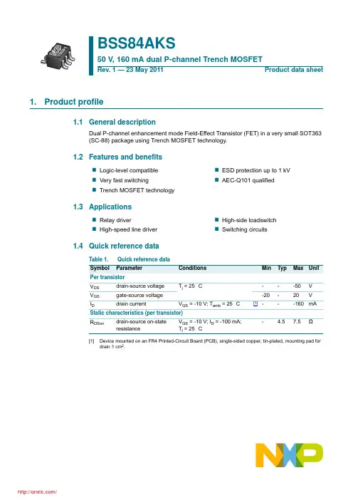
BSS84AKS,115;中文规格书,Datasheet资料
1.Product profile1.1General descriptionDual P-channel enhancement mode Field-Effect Transistor (FET) in a very small SOT363 (SC-88) package using Trench MOSFET technology.1.2Features and benefitsLogic-level compatible Very fast switchingTrench MOSFET technologyESD protection up to 1 kV AEC-Q101 qualified1.3ApplicationsRelay driverHigh-speed line driverHigh-side loadswitch Switching circuits1.4Quick reference data[1]Device mounted on an FR4 Printed-Circuit Board (PCB), single-sided copper, tin-plated, mounting pad for drain 1 cm 2.BSS84AKS50 V, 160 mA dual P-channel Trench MOSFETRev. 1 — 23 May 2011Product data sheetTable 1.Quick reference data Symbol ParameterConditions Min Typ Max Unit Per transistorV DS drain-source voltage T j =25°C---50V V GS gate-source voltage -20-20VI D drain currentV GS =-10V;T amb =25°C [1]---160mA Static characteristics (per transistor)R DSondrain-source on-state resistanceV GS =-10V;I D =-100mA; T j =25°C-4.57.5Ω2.Pinning information3.Ordering information4.Marking[1]% = placeholder for manufacturing site codeTable 2.Pinning information Pin Symbol Description Simplified outline Graphic symbol1S1source 1SOT363 (TSSOP6)2G1gate 13D2drain 24S2source 25G2gate 26D1drain 1132456sym147G1G2Table 3.Ordering informationType numberPackage NameDescriptionVersion BSS84AKSTSSOP6plastic surface-mounted package; 6 leadsSOT363Table 4.Marking codesType number Marking code [1]BSS84AKS%VY5.Limiting valuesTable 5.Limiting valuesIn accordance with the Absolute Maximum Rating System (IEC 60134).Symbol Parameter Conditions Min Max Unit Per transistorV DS drain-source voltage T j=25°C--50VV GS gate-source voltage-2020VI D drain current V GS=-10V; T amb=25°C[1]--160mAV GS=-10V; T amb=100°C[1]--100mA I DM peak drain current T amb=25°C; single pulse; t p≤10µs--640mA P tot total power dissipation T amb=25°C[2]-280mW[1]-320mWT sp=25°C-990mW Per deviceP tot total power dissipation T amb=25°C[2]-445mW T j junction temperature-55150°C T amb ambient temperature-55150°C T stg storage temperature-65150°C Source-drain diodeI S source current T amb=25°C[1]--160mA ESD maximum ratingV ESD electrostatic discharge voltage HBM[3]-1000V[1]Device mounted on an FR4 Printed-Circuit Board (PCB), single-sided copper, tin-plated, mounting pad for drain 1 cm2.[2]Device mounted on an FR4 Printed-Circuit Board (PCB), single-sided copper, tin-plated and standard footprint.[3]Measured between all pins.6.Thermal characteristicsTable 6.Thermal characteristicsSymbol Parameter Conditions Min Typ Max Unit Per deviceR th(j-a)thermal resistance from junction to ambient in free air[1]--300K/W Per transistorR th(j-a)thermal resistance from junction to ambient in free air[1]-390445K/W[2]-340390K/W R th(j-sp)thermal resistance from junction to solder point--130K/W[1]Device mounted on an FR4 PCB, single-sided copper, tin-plated and standard footprint.[2]Device mounted on an FR4 Printed-Circuit Board (PCB), single-sided copper, tin-plated, mounting pad for drain 1 cm2.7.CharacteristicsTable 7.CharacteristicsSymbol Parameter Conditions Min Typ Max Unit Static characteristics (per transistor)V(BR)DSS drain-source breakdownvoltageI D=-10µA; V GS=0V;T j=25°C-50--VV GSth gate-source thresholdvoltageI D=-250µA; V DS=V GS; T j=25°C-1.1-1.6-2.1VI DSS drain leakage current V DS=-50V; V GS=0V; T j=25°C---1µAV DS=-50V; V GS=0V; T j=150°C---2µA I GSS gate leakage current V GS=-20V;V DS=0V; T j=25°C---10µAV GS=20V;V DS=0V; T j=25°C---10µAR DSon drain-source on-stateresistance V GS=-10V;I D=-100mA; T j=25°C- 4.57.5ΩV GS=-10V;I D=-100mA; T j=150°C-813.5ΩV GS=-5V; I D=-100mA; T j=25°C- 5.78.5Ωg fs forward transconductance V DS=-10V; I D=-100mA; T j=25°C-150-mS Dynamic characteristics (per transistor)Q G(tot)total gate charge V DS=-25V; I D=-200mA; V GS=-5V;T j=25°C -0.260.35nCQ GS gate-source charge-0.12-nC Q GD gate-drain charge-0.09-nCC iss input capacitance V DS=-25V; f=1MHz; V GS=0V;T j=25°C -2436pFC oss output capacitance- 4.5-pF C rss reverse transfercapacitance- 1.3-pFt d(on)turn-on delay time V DS=-30V; R L=250Ω; V GS=-10V;R G(ext)=6Ω; T j=25°C -1326nst r rise time-11-ns t d(off)turn-off delay time-4896ns t f fall time-25-ns Source-drain diode (per transistor)V SD source-drain voltage I S=-115mA; V GS=0V; T j=25°C-0.48-0.85-1.2V分销商库存信息: NXPBSS84AKS,115。
NP311产品手册
简介NP311是一款可以让原有RS-232、RS-485、RS-422 串行设备,如门禁系统、考勤系统、保全系统、PLC、CNC、仪控设备…等,立即具备连网能力的高性能串口设备联网服务器。
NP311一方面从以太网获取UDP或TCP数据包,经内部解包提取数据后按NP311的串口设置要求由RS-232/485/422接口发送出去。
另一方面NP311从RS-232/485/422接口获取数据,在NP311内部打包成UDP或TCP数据格式经以太网口发送给目的设备。
NP311采用8位RISC单片机,提供一个RS-232串口,一个RS-484/422共用端子,安装随附于NP311的Serial 程序组后,可对其进行设置、韧件升级。
同时,使用程序组中的虚拟串口软件,用户可以在Windows操作系统中创建出与真实串口无区别的虚拟串口,用户可不需修改原有基于COM通讯软件。
同时,提供简单的联网方式,不但无需改变现有的硬件设备,而且保证了未来网络的扩充,通过简单的设置就可以实现串行设备的立即联网,支持串行与网络接口之间双向传输数据。
选择NP311,可以让您通过网络集中管理分散的串行设备,也可以通过网络管理分散的主机,满足您简易、方便的使用需求。
专注通信传输领域,力创行业领导品牌!使用须知NP311串口联网服务器在设计使用范围内具有良好可靠的性能,但仍应避免自然、人为对设备造成的损害或破坏。
请注意如下问题*请认真阅读本产品手册,并保存好本手册,以备将来使用参考*不要将设备放在近水源或潮湿的地方;*不要使用重物或硬物敲打本设备;*不要将设备放置在易雷击的地方;*不要自己修理本设备,如需修理请与供应商联系;*在下列情况下,请立即断开电源,并与供应商联系;1.设备进水;2.设备摔坏或机壳损坏;3.设备工作异常或设备性能完全改变;注意本公司有权更改产品性能及本手册内容而不事先通知客户。
在质保期内由于产品本身质量而造成不能正常使用的,本公司负责维修或进行更换,回收的产品归本公司所有。
LM311中文资料_数据手册_参数
D Fast Response Times D Strobe Capability D Maximum Input Bias Current . . . 300 nA D Maximum Input Offset Current . . . 70 nA
LM311D LM311DR LM311PSR
LM311 L311
TSSOP (PW)
Reel of 150 Tube of 2000
LM311PW LM311PWR
L311
PDIP (P)
Tube of 50
LM211P
LM211P
–40°C to 85°C
3 mV
SOIC (D)
Tube of 75 Reel of 2500
SLCS007H – SEPTEMBER 1973 – REVISED AUGUST 2003
D Can Operate From Single 5-V Supply D Available in Q-Temp Automotive
– High-Reliability Automotive Applications – Configuration Control/Print Support – Qualification to Automotive Standards
LM111 . . . JG PACKAGE LM211 . . . D, P, OR PW PACKAGE LM311 . . . D, P, PS, OR PW PACKAGE
(TOP VIEW)
EMIT OUT 1 IN+ 2 IN– 3
BS311 511系列网络控制器说明书V1.0
BS311 单门网络控制器BS511 单门网络控制器ACCESS CONTROL SYSTEM TECHNICAL MANUAL产品技术手册Version 1.0对本手册所包含的所有信息,包括URL链接和其他网上资料,本公司有权未经通知,自行修改。
所举例引用的公司名称、组织机构、产品、人名以及事件,均与任何真实公司名称、组织机构、产品、人名和事件无关。
用户应遵守所有知识产权保护法律。
本手册任何部分在未经Ningbo Bostex Technology Co., Ltd 书面同意的情况下,不得以任何形式(电子媒体、影印、记录或其他)再版、存储或引用。
手册中提到的所有其他产品,其知识产权均为其相关拥有者所具有。
© 2011 Ningbo Bostex Technology Co., Ltd版权所有此产品符合以下标准:EMC Directive: 89/336/EEC中国公安部认证软件登记测评CE认证目录1. BS311/BS511单门网络控制器 (1)1.1 简介 (1)1.2 系统构成 (1)1.2.1 BS311/BS511单门网络控制器 (1)1.2.2 读卡器 (1)1.2.3 门磁 (3)1.2.4 电控锁 (3)1.2.5 开门按钮 (3)1.2.6 其它输入/输出设备 (3)1.2.7 电源 (4)1.2.8 与PC机相连接 (4)2. 安装 (4)2.1 BS311/BS511控制器接线图 (4)2.2 与计算机连接 (4)2.2.1 通过TCP/IP与计算机连接 (4)2.2.2 通过485与计算机连接 (6)2.3 与读卡器的连接 (6)2.4 与电控锁相连接 (8)2.5 与门磁的连接 (9)2.6 与开门按钮的连接 (9)2.7 与报警继电器的连接 (9)2.8 与报警输入点的连接 (9)2.9 与电源和备用电池的连接 (10)2.10 给BS311/BS511控制器通电 (10)3. 菜单操作 (11)3.1 第一次使用 (11)3.1.1 超级用户 (12)3.1.1.1 设置超级用户密码 (12)3.1.1.2 修改超级用户密码 (12)3.1.2 管理员 (13)3.1.3 普通用户 (13)3.1.3.1 增加和删除用户 (14)3.1.3.2 更改卡片群组 (14)3.1.3.3 设置有效和失效日期 (14)3.1.3.4 禁止卡片 (15)3.2 系统设置 (15)3.2.1 以太网地址 (15)3.2.1.1 IP地址 (15)3.2.1.2 子网掩码 (15)3.2.1.3 网关 (16)3.2.1.4 MAC地址 (16)3.2.2 机号 (16)3.2.3 日期/时间设置 (17)3.2.4 搜寻子设备 (17)3.2.5 上位机通讯 (17)3.2.6 GIC服务器通讯 (19)3.2.7 防撬监控 (19)3.2.8 高级设置 (19)3.2.8.1 LCD对比度 (19)3.2.8.2 语言设置 (20)3.2.8.3 系统初始化 (20)3.2.8.4 重发所有记录 (20)3.2.8.5 删除所有记录 (20)3.2.8.6 系统支持 (21)3.2.8.7 端口通讯速率 (21)3.2.8.8 按键超时 (21)3.2.8.9 背光控制 (22)3.2.8.10 看门狗监控 (22)3.2.8.11 禁止蜂鸣器提示 (22)3.2.8.12 输出时间单位 (23)3.3 时区设置 (23)3.3.1 时段 (23)3.3.2 时区 (24)3.3.3 时区表 (24)3.4 假日设置 (25)3.5 门设置 (25)3.5.1 开门时间 (26)3.5.2 开门超时时间 (26)3.5.3 工作模式 (27)3.5.4 自动开门设置 (27)3.5.5 卡密码取消时区表 (28)3.5.6 双卡认证设置 (29)3.5.7 APB设置 (30)3.5.8 安全密码设置 (32)3.5.9 输入卡号开门 (34)3.5.10 高级设置 (34)3.5.10.1 门传感器设置 (34)3.5.10.2 方向管制 (36)3.5.10.3 密码输入错误管制 (36)3.5.10.4 记录确定 (37)3.5.10.5 报警输出点设置 (37)3.5.10.6 报警输入点设置 (39)3.5.10.7 布防设置 (40)3.5.10.8 开关门设置 (41)3.5.10.9 出门按钮控制 (41)3.5.10.10 上电时门状态复位 (42)3.5.10.11 TTL输出设置 (42)3.6 群组设置 (42)3.7 卡片设置 (43)3.7.1 同卡延迟 (43)3.7.2 显示格式 (44)3.7.3 处理格式 (44)3.7.4 自由韦根格式 (44)3.7.5 显示卡号 (45)3.7.6 控制组 (45)3.7.7 Interbus (46)3.8 其他 (46)3.8.1 更改用户密码 (46)3.8.2 同步控制器数据 (47)3.8.3 系统布防 (47)3.9 查询 (47)3.9.1 机号 (48)3.9.2 层级 (48)3.9.3 通讯状态 (48)3.9.4 子设备数量 (48)3.9.5 记录数量 (48)3.9.6 卡片数量 (48)3.9.7 固件版本号 (48)3.9.8 高级信息 (48)3.10 菜单一览表 (48)附录1 电缆规格 (51)附录2 电源规格 (52)附录3 控制器后盖安装尺寸 (53)附录4 菜单默认值一览表 (55)上电时门状态复位 (56)1. BS311/BS511单门网络控制器1.1 简介本手册讲述了BS311/BS511控制器安装及使用规范。
LM311 pdf
ELECTRICAL CHARACTERISTICS (VCC=+15 V, VEE= -15 V, TA =+25°C unless otherwise noted
[Note 1]) Symbol VIO IIO IIB Parameter Input Offset Voltage (Note 2) Input Offset Current (Note 2) Input Bias Current Test Conditions RS ≤ 50 kΩ, TA = +25°C RS ≤ 50 kΩ, -45°C ≤ TA ≤ 85°C TA = +25°C -45°C ≤ TA ≤ 85°C TA = +25°C TA = -45°C TA = +85°C 150000 300 TA = +25°C VID ≤ -10 mV, IO=50 mA -14.5 1.5 13.0 +7.5 -5.0 ns V V mA mA Guaranteed Limits Min Max 7.5 10 50 100 250 375 500 mV nA nA Unit
2
This datasheet has been downloaded from:
Free Download Daily Updated Database 100% Free Datasheet Search Site 100% Free IC Replacement Search Site Convenient Electronic Dictionary Fast Search System
AV tDLH VDS VIR ICC IEE
Voltage Gain Propagation Delay Time Saturation Voltage Input Voltage Range Positive Supply Current Negative Supply Current