FPGA可编程逻辑器件芯片XC7VX690T-L2FFG1926E中文规格书
FPGA可编程逻辑器件芯片XC7VX690T-3FF1926E中文规格书

7Series FPGAs Data Sheet: OverviewDS180 (v2.6.1) September 8, 2020Product SpecificationKintex-7 FPGA Feature SummaryTable 6:Kintex-7 FPGA Feature Summary by Device Device Logic Cells Configurable Logic Blocks (CLBs)DSP Slices (2)Block RAM Blocks (3)CMTs (4)PCIe (5)GTXs XADC Blocks Total I/O Banks (6)Max User I/O (7)Slices (1)Max Distributed RAM (Kb)18Kb 36Kb Max (Kb)XC7K70T 65,60010,2508382402701354,86061816300XC7K160T 162,24025,3502,18860065032511,70081818400XC7K325T 326,08050,9504,00084089044516,02010116110500XC7K355T 356,16055,6505,0881,4401,43071525,740612416300XC7K410T 406,72063,5505,6631,5401,59079528,62010116110500XC7K420T 416,96065,1505,9381,6801,67083530,060813218400XC7K480T 477,76074,6506,7881,9201,91095534,380813218400Notes:1.Each 7series FPGA slice contains four LUTs and eight flip-flops; only some slices can use their LUTs as distributed RAM or SRLs.2.Each DSP slice contains a pre-adder, a 25x 18 multiplier, an adder, and an accumulator.3.Block RAMs are fundamentally 36Kb in size; each block can also be used as two independent 18 Kb blocks.4.Each CMT contains one MMCM and one PLL.5.Kintex-7 FPGA Interface Blocks for PCI Express support up to x8 Gen 2.6.Does not include configuration Bank 0.7.This number does not include GTX transceivers.Table 7:Kintex-7 FPGA Device-Package Combinations and Maximum I/OsPackage (1)FBG484 FBG676(2)FFG676(2) FBG900(3)FFG900(3)FFG901FFG1156Size (mm)23 x 2327 x 2727 x 2731 x 3131 x 3131 x 3135 x 35Ball Pitch (mm)1.0 1.0 1.0 1.0 1.0 1.0 1.0DeviceGTX (4)I/O GTX (4)I/O GTX I/O GTX (4)I/O GTX I/O GTX I/O GTX I/O HR (5)HP (6)HR (5)HP (6)HR (5)HP (6)HR (5)HP (6)HR (5)HP (6)HR (5)HP (6)HR (5)HP (6)XC7K70T41851008200100XC7K160T418510082501508250150XC7K325T825015082501501635015016350150XC7K355T243000XC7K410T825015082501501635015016350150XC7K420T283800324000XC7K480T 283800324000Notes:1.All packages listed are Pb-free (FBG, FFG with exemption 15). Some packages are available in Pb option.2.Devices in FBG676 and FFG676 are footprint compatible.3.Devices in FBG900 and FFG900 are footprint compatible.4.GTX transceivers in FB packages support the following maximum data rates: 10.3Gb/s in FBG484; 6.6Gb/s in FBG676 and FBG900. Refer to Kintex-7 FPGAs Data Sheet:DC and AC Switching Characteristics (DS182) for details.5.HR = High-range I/O with support for I/O voltage from 1.2V to 3.3V.6.HP = High-performance I/O with support for I/O voltage from 1.2V to 1.8V.7Series FPGAs Data Sheet: OverviewBlock RAMSome of the key features of the block RAM include:•Dual-port 36Kb block RAM with port widths of up to 72•Programmable FIFO logic•Built-in optional error correction circuitryEvery 7series FPGA has between 5 and 1,880 dual-port block RAMs, each storing 36Kb. Each block RAM has two completely independent ports that share nothing but the stored data.Synchronous OperationEach memory access, read or write, is controlled by the clock. All inputs, data, address, clock enables, and write enables are registered. Nothing happens without a clock. The input address is always clocked, retaining data until the next operation. An optional output data pipeline register allows higher clock rates at the cost of an extra cycle of latency.During a write operation, the data output can reflect either the previously stored data, the newly written data, or can remain unchanged.Programmable Data WidthEach port can be configured as 32K×1, 16K×2, 8K×4, 4K×9 (or8), 2K×18 (or16), 1K×36 (or32), or 512×72 (or64). The two ports can have different aspect ratios without any constraints.Each block RAM can be divided into two completely independent 18Kb block RAMs that can each be configured to any aspect ratio from 16K×1 to 512×36. Everything described previously for the full 36Kb block RAM also applies to each of the smaller 18Kb block RAMs.Only in simple dual-port (SDP) mode can data widths of greater than 18bits (18Kb RAM) or 36bits (36Kb RAM) be accessed. In this mode, one port is dedicated to read operation, the other to write operation. In SDP mode, one side (read or write) can be variable, while the other is fixed to 32/36 or 64/72.Both sides of the dual-port 36Kb RAM can be of variable width.Two adjacent 36Kb block RAMs can be configured as one cascaded 64K×1 dual-port RAM without any additional logic. Error Detection and CorrectionEach 64-bit-wide block RAM can generate, store, and utilize eight additional Hamming code bits and perform single-bit error correction and double-bit error detection (ECC) during the read process. The ECC logic can also be used when writing to or reading from external 64- to 72-bit-wide memories.FIFO ControllerThe built-in FIFO controller for single-clock (synchronous) or dual-clock (asynchronous or multirate) operation increments the internal addresses and provides four handshaking flags: full, empty, almost full, and almost empty. The almost full and almost empty flags are freely programmable. Similar to the block RAM, the FIFO width and depth are programmable, but the write and read ports always have identical width.First word fall-through mode presents the first-written word on the data output even before the first read operation. After the first word has been read, there is no difference between this mode and the standard mode.DS180 (v2.6.1) September 8, 2020Product Specification。
FPGA可编程逻辑器件芯片XC7VX690T-3FFG1926I中文规格书

Virtex-5 Family OverviewDS100 (v5.1) August 21, 2015Product SpecificationDigitally Controlled Impedance (DCI)Active I/O Termination•Optional series or parallel termination •Temperature and voltage compensation •Makes board layout much easier−Reduces resistors −Places termination in the ideal location, at the signalsource or destination Configuration •Support for platform Flash, standard SPI Flash, or standard parallel NOR Flash configuration •Bitstream support with dedicated fallback reconfiguration logic •256-bit AES bitstream decryption provides intellectual property security and prevents design copying •Improved bitstream error detection/correction capability •Auto bus width detection capability •Partial Reconfiguration via ICAP port Advanced Flip-Chip Packaging •Pre-engineered packaging technology for proven superior signal integrity−Minimized inductive loops from signal to return −Optimal signal-to-PWR/GND ratios •Reduces SSO induced noise by up to 7x •Pb-Free and standard packages System Monitor •On-Chip temperature measurement (±4°C)•On-Chip power supply measurement (±1%)•Easy to use, self-contained −No design required for basic operation −Autonomous monitoring of all on-chip sensors −User programmable alarm thresholds for on-chip sensors•User accessible 10-bit 200kSPS ADC −Automatic calibration of offset and gain error −DNL = ±0.9 LSBs maximum •Up to 17 external analog input channels supported −0V to 1V input range −Monitor external sensors e.g., voltage, temperature −General purpose analog inputs •Full access from fabric or JT AG TAP to System Monitor •Fully operational prior to FPGA configuration and during device power down (access via JTAG T AP only)65-nm Copper CMOS Process • 1.0V Core Voltage •12-layer metal provides maximum routing capability and accommodates hard-IP immersion •Triple-oxide technology for proven reduced static power consumption System Blocks Specific to the LXT, SXT, TXT, and FXT DevicesIntegrated Endpoint Block for PCI ExpressCompliance•Works in conjunction with RocketIO GTP transceivers (LXT and SXT) and GTX transceivers (TXT and FXT)to deliver full PCI Express Endpoint functionality withminimal FPGA logic utilization.•Compliant with the PCI Express Base Specification 1.1•PCI Express Endpoint block or Legacy PCI Express Endpoint block•x8, x4, or x1 lane width •Power management support •Block RAMs used for buffering •Fully buffered transmit and receive •Management interface to access PCI Express configuration space and internal configuration•Supports the full range of maximum payload sizes •Up to 6x 32 bit or 3x 64 bit BARs (or a combination of 32 bit and 64 bit)Tri-Mode Ethernet Media Access Controller •Designed to the IEEE 802.3-2002 specification •Operates at 10, 100, and 1,000 Mb/s •Supports tri-mode auto-negotiation •Receive address filter (5 address entries)•Fully monolithic 1000Base-X solution with RocketIO GTP transceivers •Supports multiple external PHY connections (RGMII,GMII, etc.) interfaces through soft logic and SelectIO resources •Supports connection to external PHY device through SGMII using soft logic and RocketIO GTP transceivers •Receive and transmit statistics available through separate interface •Separate host and client interfaces •Support for jumbo frames •Support for VLAN •Flexible, user-configurable host interface •Supports IEEE 802.3ah-2004 unidirectional modeVirtex-5 Family OverviewDS100 (v5.1) August 21, 2015Product Specification Table 1:Virtex-5 FPGA Family Members Device Configurable Logic Blocks (CLBs)DSP48E Slices (2)Block RAM Blocks CMTs (4)PowerPC Processor Blocks Endpoint Blocks for PCI ExpressEthernet MACs (5)Max RocketIO Transceivers (6)Total I/O Banks (8)Max User I/O (7)Array (Row x Col)Virtex-5 Slices (1)Max Distributed RAM (Kb)18Kb (3)36Kb Max (Kb)GTP GTX XC5VLX3080x 304,8003203264321,1522N/A N/A N/A N/A N/A 13400XC5VLX50120x 307,2004804896481,7286N/A N/A N/A N/A N/A 17560XC5VLX85120x 5412,96084048192963,4566N/A N/A N/A N/A N/A 17560XC5VLX110160x 5417,2801,120642561284,6086N/A N/A N/A N/A N/A 23800XC5VLX155160x 7624,3201,6401283841926,9126N/A N/A N/A N/A N/A 23800XC5VLX220160x 10834,5602,2801283841926,9126N/A N/A N/A N/A N/A 23800XC5VLX330240x 10851,8403,42019257628810,3686N/A N/A N/A N/A N/A 331,200XC5VLX20T60x 263,1202102452269361N/A 124N/A 7172XC5VLX30T80x 304,8003203272361,2962N/A 148N/A 12360XC5VLX50T120x 307,20048048120602,1606N/A 1412N/A 15480XC5VLX85T120x 5412,960840482161083,8886N/A 1412N/A 15480XC5VLX110T160x 5417,2801,120642961485,3286N/A 1416N/A 20680XC5VLX155T 160x 7624,3201,6401284242127,6326N/A 1416N/A 20680XC5VLX220T 160x 10834,5602,2801284242127,6326N/A 1416N/A 20680XC5VLX330T 240x 10851,8403,42019264832411,6646N/A 1424N/A 27960XC5VSX35T 80x 345,440520192168843,0242N/A 148N/A 12360XC5VSX50T 120x 348,1607802882641324,7526N/A 1412N/A 15480XC5VSX95T 160x 4614,7201,5206404882448,7846N/A 1416N/A 19640XC5VSX240T 240x 7837,4404,2001,0561,03251618,5766N/A 1424N/A 27960XC5VTX150T 200x 5823,2001,500804562288,2086N/A 14N/A 4020680XC5VTX240T 240x 7837,4402,4009664832411,6646N/A 14N/A 4820680XC5VFX30T 80x 385,12038064136682,4482114N/A 812360XC5VFX70T 160x 3811,2008201282961485,3286134N/A 1619640XC5VFX100T 160x 5616,0001,2402564562288,2086234N/A 1620680XC5VFX130T 200x 5620,4801,58032059629810,7286236N/A 2024840XC5VFX200T 240x 6830,7202,28038491245616,4166248N/A 2427960Notes:1.Virtex-5 FPGA slices are organized differently from previous generations. Each Virtex-5 FPGA slice contains four LUTs and four flip-flops (previously it was two LUTs and two flip-flops.)2.Each DSP48E slice contains a 25x 18 multiplier, an adder, and an accumulator.3.Block RAMs are fundamentally 36Kbits in size. Each block can also be used as two independent 18-Kbit blocks.4.Each Clock Management Tile (CMT) contains two DCMs and one PLL.5.This table lists separate Ethernet MACs per device.6.RocketIO GTP transceivers are designed to run from 100Mb/s to 3.75Gb/s. RocketIO GTX transceivers are designed to run from 150Mb/s to 6.5Gb/s.7.This number does not include RocketIO transceivers.8.Includes configuration Bank 0.。
FPGA可编程逻辑器件芯片XC7VX690T-2FFG1926E中文规格书

DS180 (v2.6.1) September 8, 2020Product SpecificationGeneral DescriptionXilinx® 7series FPGAs comprise four FPGA families that address the complete range of system requirements, ranging from low cost, small form factor, cost-sensitive, high-volume applications to ultra high-end connectivity bandwidth, logic capacity, and signal processing capability for the most demanding high-performance applications. The 7series FPGAs include:•Spartan®-7 Family: Optimized for low cost, lowest power, and highI/O performance. Available in low-cost, very small form-factorpackaging for smallest PCB footprint.•Artix®-7 Family: Optimized for low power applications requiring serialtransceivers and high DSP and logic throughput. Provides the lowesttotal bill of materials cost for high-throughput, cost-sensitiveapplications.•Kintex®-7 Family: Optimized for best price-performance with a 2X improvement compared to previous generation, enabling a new class of FPGAs.•Virtex®-7 Family: Optimized for highest system performance and capacity with a 2X improvement in system performance. Highest capability devices enabled by stacked silicon interconnect (SSI)technology.Built on a state-of-the-art, high-performance, low-power (HPL), 28nm, high-k metal gate (HKMG) process technology, 7series FPGAs enable an unparalleled increase in system performance with 2.9Tb/s of I/O bandwidth, 2 million logic cell capacity, and 5.3TMAC/s DSP, while consuming 50% less power than previous generation devices to offer a fully programmable alternative to ASSPs and ASICs.Summary of 7Series FPGA Features•Advanced high-performance FPGA logic based on real 6-input look-up table (LUT) technology configurable as distributed memory.•36Kb dual-port block RAM with built-in FIFO logic for on-chip data buffering.•High-performance SelectIO™ technology with support for DDR3interfaces up to 1,866 Mb/s.•High-speed serial connectivity with built-in multi-gigabit transceivers from 600Mb/s to max. rates of 6.6Gb/s up to 28.05Gb/s, offering a special low-power mode, optimized for chip-to-chip interfaces.•A user configurable analog interface (XADC), incorporating dual 12-bit 1MSPS analog-to-digital converters with on-chip thermal and supply sensors.•DSP slices with 25x 18 multiplier, 48-bit accumulator, and pre-adder for high-performance filtering, including optimized symmetric coefficient filtering.•Powerful clock management tiles (CMT), combining phase-locked loop (PLL) and mixed-mode clock manager (MMCM) blocks for high precision and low jitter.•Quickly deploy embedded processing with MicroBlaze™ processor.•Integrated block for PCI Express® (PCIe), for up to x8 Gen3Endpoint and Root Port designs.•Wide variety of configuration options, including support for commodity memories, 256-bit AES encryption with HMAC/SHA-256authentication, and built-in SEU detection and correction.•Low-cost, wire-bond, bare-die flip-chip, and high signal integrity flip-chip packaging offering easy migration between family members in the same package. All packages available in Pb-free and selected packages in Pb option.•Designed for high performance and lowest power with 28nm,HKMG, HPL process, 1.0V core voltage process technology and 0.9V core voltage option for even lower power.7Series FPGAs Data Sheet: OverviewDS180 (v2.6.1) September 8, 2020Product Specification Table 1:7Series Families Comparison Max. CapabilitySpartan-7Artix-7Kintex-7Virtex-7Logic Cells102K 215K 478K 1,955K Block RAM (1)4.2Mb 13Mb 34Mb 68Mb DSP Slices1607401,9203,600DSP Performance (2)176 GMAC/s 929GMAC/s 2,845GMAC/s 5,335GMAC/s MicroBlaze CPU (3)260 DMIPs 303 DMIPs 438 DMIPs 441 DMIPs Transceivers–163296Transceiver Speed– 6.6Gb/s 12.5Gb/s 28.05Gb/s Serial Bandwidth–211Gb/s 800Gb/s 2,784Gb/s PCIe Interface–x4 Gen2x8 Gen2x8 Gen3Memory Interface800Mb/s 1,066Mb/s 1,866Mb/s 1,866Mb/s I/O Pins400500500 1,200I/O Voltage1.2V–3.3V 1.2V–3.3V 1.2V–3.3V 1.2V–3.3V Package OptionsLow-Cost, Wire-Bond Low-Cost, Wire-Bond, Bare-Die Flip-Chip Bare-Die Flip-Chip and High-Performance Flip-Chip Highest Performance Flip-ChipNotes:1.Additional memory available in the form of distributed RAM.2.Peak DSP performance numbers are based on symmetrical filter implementation.3.Peak MicroBlaze CPU performance numbers based on microcontroller preset.7Series FPGAs Data Sheet: OverviewDS180 (v2.6.1) September 8, 2020Product Specification Spartan-7 FPGA Feature SummaryTable 2:Spartan-7 FPGA Feature Summary by Device Device Logic CellsCLBDSP Slices (2)Block RAM Blocks (3) CMTs (4)PCIe GT XADC Blocks Total I/O Banks (5)Max User I/O Slices (1)Max Distributed RAM (Kb)18Kb 36Kb Max (Kb)XC7S66,000938701010518020002100XC7S1512,8002,00015020201036020002100XC7S2523,3603,6503138090451,62030013150XC7S5052,1608,150600120150752,70050015250XC7S7576,80012,000832140180903,24080018400XC7S100102,40016,0001,1001602401204,32080018400Notes:1.Each 7series FPGA slice contains four LUTs and eight flip-flops; only some slices can use their LUTs as distributed RAM or SRLs.2.Each DSP slice contains a pre-adder, a 25x 18 multiplier, an adder, and an accumulator.3.Block RAMs are fundamentally 36Kb in size; each block can also be used as two independent 18Kb blocks.4.Each CMT contains one MMCM and one PLL.5.Does not include configuration Bank 0.Table 3:Spartan-7 FPGA Device-Package Combinations and Maximum I/OsPackageCPGA196CSGA225CSGA324FTGB196FGGA484FGGA676Size (mm)8 x 813 x 1315 x 1515 x 1523 x 2327 x 27Ball Pitch (mm)0.50.80.8 1.0 1.0 1.0DeviceHR I/O (1)HR I/O (1)HR I/O (1)HR I/O (1)HR I/O (1)HR I/O (1)XC7S6100100100XC7S15100100100XC7S25150150100XC7S50210100250XC7S75338400XC7S100338400Notes:1.HR = High-range I/O with support for I/O voltage from 1.2V to 3.3V.。
FPGA可编程逻辑器件芯片XC7VX690T-3FFG1927I中文规格书
Virtex-5 Family OverviewDS100 (v5.1) August 21, 2015Product SpecificationVirtex-5 TXT and FXT Platform FeaturesThis section describes blocks only available in TXT and FXT devices.RocketIO GTX Serial Transceivers(TXT/FXT)8-48 channels RocketIO serial transceivers capable ofrunning 150Mb/s to 6.5Gb/s•Full Clock and Data Recovery •8/16/32-bit or 10/20/40-bit datapath support •Optional 8B/10B encoding, gearbox for programmable 64B/66B or 64B/67B encoding, or FPGA-basedencode/decode •Integrated FIFO/Elastic Buffer •Channel bonding and clock correction support •Dual embedded 32-bit CRC generation/checking •Integrated programmable character detection •Programmable de-emphasis (AKA transmitter equalization)•Programmable transmitter output swings •Programmable receiver equalization •Programmable receiver termination •Embedded support for:−Serial A T A: Out of Band (OOB) signalling −PCI Express: Beaconing, electrical idle, and receiverdetection •Built-in PRBS generator/checker Virtex-5 FPGA RocketIO GTX transceivers are furtherdiscussed in the Virtex-5 FPGA RocketIO GTX T ransceiver User Guide .One or Two PowerPC 440 Processor Cores (FXT only)•Superscalar RISC architecture •32-bit Book E compliant •7-Stage execution pipeline •Multiple instructions per cycle •Out-of-order execution •Integrated 32KB Level 1 Instruction Cache and 32KB Level 1 Data Cache (64-way set associative)•CoreConnect™ Bus Architecture •Cross-bar connection for optimized processor bandwidth •PLB Synchronization Logic (Enables non-integer CPU-to-PLB clock ratios)•Auxiliary Processor Unit (APU) interface with an integrated APU controller −Optimized FPGA-based Coprocessor connection -Automatic decode of PowerPC floating-point instructions −Allows custom instructions −Extremely efficient microcontroller-style interfacingThe PowerPC 440 processors are further discussed in the Embedded Processor Block in Virtex-5 FPGAs Reference Guide .Intellectual Property CoresXilinx offers IP cores for commonly used complex functionsincluding DSP , bus interfaces, processors, and processorperipherals. Using Xilinx LogiCORE™ products and cores fromthird party AllianceCORE participants, customers can shortendevelopment time, reduce design risk, and obtain superiorperformance for their designs. Additionally, the CORE Generator™ system allows customers to implement IP cores into Virtex-5FPGAs with predictable and repeatable performance. It offers asimple user interface to generate parameter-based coresoptimized for our FPGAs.The System Generator for DSP tool allows system architects toquickly model and implement DSP functions using handcrafted IP and features an interface to third-party system level DSP designtools. System Generator for DSP implements many of the high-performance DSP cores supporting Virtex-5 FPGAs including the Xilinx Forward Error Correction Solution with Interleaver/De-interleaver, Reed-Solomon encoder/decoders, and Viterbidecoders. These are ideal for creating highly-flexible,concatenated codecs to support the communications market.Using Virtex-5 FPGA RocketIO transceivers, industry leadingconnectivity and networking IP cores include leading-edge PCIExpress, Serial RapidIO, Fibre Channel, and 10Gb Ethernetcores can be implemented. The Xilinx SPI-4.2 IP core utilizes the Virtex-5 FPGA ChipSync technology to implement dynamic phase alignment for high-performance source-synchronous operation. Xilinx also provides PCI cores for advanced system-synchronous operation.The MicroBlaze™ 32-bit processor core provides the industry's fastest soft processing solution for building complex systems for the networking, telecommunication, data communication, embedded, and consumer markets. The MicroBlaze processor features a RISC architecture with Harvard-style separate 32-bit instruction and data buses running at full speed to execute programs and access data from both on-chip and external memory. A standard set of peripherals are also CoreConnect™ enabled to offer MicroBlaze designers compatibility and reuse.All IP cores for Virtex-5 FPGAs are found on the Xilinx IP Center Internet portal presenting the latest intellectual property cores and reference designs using Smart Search for faster access.Virtex-5 FPGA LogiCORE Endpoint Block Plus Wrapper for PCI Express This is the recommended wrapper to configure the integrated Endpoint block for PCI Express delivered through the CORE Generator system. It provides many ease-of-use features and optimal configuration for Endpoint application simplifying the design process and reducing the time-to-market. Access to the core, including bitstream generation capability can be obtained through registration at no extra charge.Virtex-5 Family OverviewDS100 (v5.1) August 21, 2015Product Specification RocketIO GTP Transceivers (LXT/SXT only)•Full-duplex serial transceiver capable of 100Mb/s to 3.75Gb/s baud rates •8B/10B, user-defined FPGA logic, or no encoding options •Channel bonding support •CRC generation and checking •Programmable pre-emphasis or pre-equalization for the transmitter •Programmable termination and voltage swing •Programmable equalization for the receiver •Receiver signal detect and loss of signal indicator •User dynamic reconfiguration using secondary configuration bus •Out of Band (OOB) support for Serial AT A (SAT A)•Electrical idle, beaconing, receiver detection, and PCI Express and SATA spread-spectrum clocking support •Less than 100mW typical power consumption •Built-in PRBS Generators and Checkers RocketIO GTX Transceivers (TXT/FXT only)•Full-duplex serial transceiver capable of 150Mb/s to 6.5Gb/s baud rates •8B/10B encoding and programmable gearbox to support 64B/66B and 64B/67B encoding, user-definedFPGA logic, or no encoding options•Channel bonding support•CRC generation and checking•Programmable pre-emphasis or pre-equalization for the transmitter•Programmable termination and voltage swing•Programmable continuous time equalization for the receiver•Programmable decision feedback equalization for the receiver•Receiver signal detect and loss of signal indicator •User dynamic reconfiguration using secondary configuration bus•OOB support (SAT A)•Electrical idle, beaconing, receiver detection, and PCI Express spread-spectrum clocking support •Low-power operation at all line rates PowerPC 440 RISC Cores (FXT only)•Embedded PowerPC 440 (PPC440) cores −Up to 550MHz operation −Greater than 1000 DMIPS per core −Seven-stage pipeline −Multiple instructions per cycle −Out-of-order execution −32Kbyte, 64-way set associative level 1 instruction cache −32Kbyte, 64-way set associative level 1 data cache −Book E compliant •Integrated crossbar for enhanced system performance −128-bit Processor Local Buses (PLBs)−Integrated scatter/gather DMA controllers −Dedicated interface for connection to DDR2 memory controller −Auto-synchronization for non-integer PLB-to-CPU clock ratios •Auxiliary Processor Unit (APU) Interface and Controller −Direct connection from PPC440 embedded block to FPGA fabric-based coprocessors −128-bit wide pipelined APU Load/Store −Support of autonomous instructions: no pipeline stalls −Programmable decode for custom instructions。
FPGA可编程逻辑器件芯片XQ7VX690T-2RF1157I中文规格书

General DescriptionXilinx® Defense-grade 7series FPGAs comprise three FPGA families that address the complete range of system requirements, ranging from low cost, small form factor, cost-sensitive, high-volume applications to ultra high-end connectivity bandwidth, logic capacity, and signal processing capability for the high reliability requirements beyond commercial applications. The Defense-grade 7series FPGAs include:•Artix®-7Q Family: Optimized for lowest cost and power with small form-factor packaging for the highest volume applications.•Kintex®-7Q Family: Optimized for best price-performance with a 2X improvement compared to previous generation, enabling a new class of FPGAs.•Virtex®-7Q Family: Optimized for highest system performance and capacity with a 2X improvement in system performance.Built on a state-of-the-art, high-performance, low-power (HPL), 28nm, high-k metal gate (HKMG) process technology, Defense-grade 7series FPGAs enable an unparalleled increase in system performance with 1.4Tb/s of I/O bandwidth, 980K logic cell capacity, and 4.7TMAC/s DSP, while consuming 50% less power than previous generation devices to offer a fully programmable alternative to ASSPs and ASICs.Summary of Defense-Grade 7Series FPGA Features•Full-range extended temperature testing•Mask set control•Fully leaded (Pb) content•Ruggedized packaging•Long-term availability•Anti-counterfeiting features•4th Generation Information Assurance and Anti-tamper support •Advanced high-performance FPGA logic based on real 6-input look-up table (LUT) technology configurable as distributed memory.•36Kb dual-port block RAM with built-in FIFO logic for on-chip data buffering.•High-performance SelectIO™ technology with support for DDR3 interfaces up to 1,866 Mb/s.•High-speed serial connectivity with built-in multi-gigabit transceivers from 600Mb/s to maximum rates of 6.6Gb/s up to 11.3Gb/s,offering a special low-power mode, optimized for chip-to-chipinterfaces.• A user configurable analog interface (XADC), incorporating dual 12-bit 1MSPS analog-to-digital converters with on-chip thermal and supply sensors.•DSP slices with 25x18 multiplier, 48-bit accumulator, and pre-adder for high performance filtering, including optimized symmetriccoefficient filtering.•Powerful clock management tiles (CMT), combining phase-locked loop (PLL) and mixed-mode clock manager (MMCM) blocks for high precision and low jitter.•Integrated block for PCI Express® (PCIe), for up to x8 Gen3 Endpoint and Root Port designs.•Wide variety of configuration options, including support for commodity memories, 256-bit AES encryption with HMAC/SHA-256 authentication, and built-in SEU detection and correction.•Wire-bond and high signal integrity lidded flip-chip ruggedized packages offering easy migration between family members in thesame package. All packages are available in Pb option.•Designed for high performance and lowest power with 28nm, HKMG, and HPL process.Defense-Grade 7Series FPGAs Overview DS185 (v1.2) July 2, 2015Product SpecificationTable 1:Defense-Grade 7Series Families ComparisonMaximum Capability Artix-7Q Family Kintex-7Q Family Virtex-7Q FamilyLogic Cells215K407K979KBlock RAM(1)13Mb27Mb54MbDSP Slices 7401,5403,600Peak DSP Performance(2)814GMAC/s2,002GMAC/s4,680GMAC/s Transceivers81648Peak Transceiver Speed 6.6Gb/s10.3125Gb/s11.3Gb/sPeak Serial Bandwidth (Full Duplex)106Gb/s330Gb/s814Gb/sPCIe Interface x4 Gen2x8 Gen2x8 Gen3Memory Interface800Mb/s1,866Mb/s1,866Mb/sI/O Pins400500 1,000I/O Voltage 1.2V, 1.35V, 1.5V, 1.8V, 2.5V, 3.3V 1.2V, 1.35V, 1.5V, 1.8V, 2.5V, 3.3V 1.2V, 1.35V, 1.5V, 1.8V, 2.5V, 3.3V Package Options Wire-Bond, Ruggedized Flip-Chip Ruggedized Flip-Chip Ruggedized Flip-Chip Notes:1.Additional memory available in the form of distributed RAM.2.Peak DSP performance numbers are based on symmetrical filter implementation.Virtex-7Q FPGA Feature Summary Table 6:Virtex-7Q FPGA Feature SummaryDevice LogicCellsConfigurable Logic Blocks(CLBs)DSPSlices(2)Block RAM Blocks(3)CMTs(4)PCIe(5)GTX GTH GTZXADCBlocksTotal I/OBanks(6)MaxUserI/O(7) Slices(1)Max DistributedRAM (Kb)18Kb36KbMax(Kb)XQ7V585T582,72091,0506,9381,260 1,590795 28,6201833600117850 XQ7VX330T326,40051,0004,3881,1201,50075027,0001420280114700 XQ7VX485T485,76075,9008,1752,8002,0601,03037,0801422800114700 XQ7VX690T693,120108,30010,8883,6002,9401,47052,92020304801201,000 XQ7VX980T979,200153,00013,8383,6003,0001,50054,0001820240118900 Notes:1.Each Defense-grade 7series FPGA slice contains four LUTs and eight flip-flops; only some slices can use their LUTs as distributed RAM or SRLs.2.Each DSP slice contains a pre-adder, a 25x18 multiplier, an adder, and an accumulator.3.Block RAMs are fundamentally 36Kb in size; each block can also be used as two independent 18 Kb blocks.4.Each CMT contains one MMCM and one PLL.5.Virtex-7Q T FPGA Interface Blocks for PCI Express support up to x8 Gen 2. Virtex-7Q XT Interface Blocks for PCI Express support up to x8 Gen 3, with the exception ofthe XQ7VX485T device, which supports x8 Gen 2.6.Does not include configuration Bank 0.7.This number does not include GTX, GTH, or GTZ transceivers.Table 7:Virtex-7Q FPGA Device-Package Combinations and Maximum I/OsPackage RF1157RF1158RF1761RF1930 Size (mm)35 x 3535 x 3542.5 x 42.545 x 45 Ball Pitch 1.0 1.0 1.0 1.0Device GTX GTHI/OGTX GTHI/OGTX GTHI/OGTX GTHI/O HR(1)HP(2)HR(1)HP(2)HR(1)HP(2)HP(1)XQ7V585T2000600360100750XQ7VX330T020060002850650XQ7VX485T2800700240700 XQ7VX690T0200600048035003608500241,000 XQ7VX980T024900Clock ManagementSome of the key highlights of the clock management architecture include:•High-speed buffers and routing for low-skew clock distribution•Frequency synthesis and phase shifting•Low-jitter clock generation and jitter filteringEach Defense-grade 7series FPGA has up to 20 clock management tiles (CMTs), each consisting of one mixed-mode clock manager (MMCM) and one phase-locked loop (PLL).Mixed-Mode Clock Manager and Phase-Locked LoopThe MMCM and PLL share many characteristics. Both can serve as a frequency synthesizer for a wide range of frequencies and as a jitter filter for incoming clocks. At the center of both components is a voltage-controlled oscillator (VCO), which speeds up and slows down depending on the input voltage it receives from the phase frequency detector (PFD).There are three sets of programmable frequency dividers: D, M, and O. The pre-divider D (programmable by configuration and afterwards via DRP) reduces the input frequency and feeds one input of the traditional PLL phase/frequency comparator. The feedback divider M (programmable by configuration and afterwards via DRP) acts as a multiplier because it divides the VCO output frequency before feeding the other input of the phase comparator. D and M must be chosen appropriately to keep the VCO within its specified frequency range. The VCO has eight equally-spaced output phases (0°, 45°, 90°, 135°, 180°, 225°, 270°, and 315°). Each can be selected to drive one of the output dividers (six for the PLL, O0 to O5, and seven for the MMCM, O0 to O6), each programmable by configuration to divide by any integer from 1 to 128.The MMCM and PLL have three input-jitter filter options: low bandwidth, high bandwidth, or optimized mode. Low-bandwidth mode has the best jitter attenuation but not the smallest phase offset. High-bandwidth mode has the best phase offset, but not the best jitter attenuation. Optimized mode allows the tools to find the best setting.MMCM Additional Programmable FeaturesThe MMCM can have a fractional counter in either the feedback path (acting as a multiplier) or in one output path. Fractional counters allow non-integer increments of 1/8 and can thus increase frequency synthesis capabilities by a factor of 8.The MMCM can also provide fixed or dynamic phase shift in small increments that depend on the VCO frequency.Clock DistributionEach Defense-grade 7series FPGA provides six different types of clock lines (BUFG, BUFR, BUFIO, BUFH, BUFMR, and the high-performance clock) to address the different clocking requirements of high fanout, short propagation delay, and extremely low skew.Global Clock LinesIn each Defense-grade 7series FPGA, 32 global clock lines have the highest fanout and can reach every flip-flop clock, clock enable, and set/reset, as well as many logic inputs. There are 12 global clock lines within any clock region driven by the horizontal clock buffers (BUFH). Each BUFH can be independently enabled/disabled, allowing for clocks to be turned off within a region, thereby offering fine-grain control over which clock regions consume power. Global clock lines can be driven by global clock buffers, which can also perform glitchless clock multiplexing and clock enable functions. Global clocks are often driven from the CMT, which can completely eliminate the basic clock distribution delay.Regional ClocksRegional clocks can drive all clock destinations in their region. A region is defined as any area that is 50 I/O and 50 CLB high and half the chip wide. Defense-grade 7series FPGAs have between six and twenty regions. There are four regional clock tracks in every region. Each regional clock buffer can be driven from either of four clock-capable input pins, and its frequency can optionally be divided by any integer from 1 to 8.Every Defense-grade 7series FPGA has between 75 and 1,500 dual-port block RAMs, each storing 36Kb. Each block RAM has two completely independent ports that share nothing but the stored data.Synchronous OperationEach memory access, read or write, is controlled by the clock. All inputs, data, address, clock enables, and write enables are registered. Nothing happens without a clock. The input address is always clocked, retaining data until the next operation. An optional output data pipeline register allows higher clock rates at the cost of an extra cycle of latency.During a write operation, the data output can reflect either the previously stored data, the newly written data, or can remain unchanged.Programmable Data WidthEach port can be configured as 32K×1, 16K×2, 8K×4, 4K×9 (or8), 2K×18 (or16), 1K×36 (or32), or 512×72 (or64). The two ports can have different aspect ratios without any constraints.Each block RAM can be divided into two completely independent 18Kb block RAMs that can each be configured to any aspect ratio from 16K×1 to 512×36. Everything described previously for the full 36Kb block RAM also applies to each of the smaller 18Kb block RAMs.Only in simple dual-port (SDP) mode can data widths of greater than 18bits (18Kb RAM) or 36bits (36Kb RAM) be accessed. In this mode, one port is dedicated to read operation, the other to write operation. In SDP mode, one side (read or write) can be variable, while the other is fixed to 32/36 or 64/72.Both sides of the dual-port 36Kb RAM can be of variable width.Two adjacent 36Kb block RAMs can be configured as one cascaded 64K×1 dual-port RAM without any additional logic. Error Detection and CorrectionEach 64-bit-wide block RAM can generate, store, and utilize eight additional Hamming code bits and perform single-bit error correction and double-bit error detection (ECC) during the read process. The ECC logic can also be used when writing to or reading from external 64- to 72-bit-wide memories.。
FPGA可编程逻辑器件芯片XC7VX690T-L2FFG1927E中文规格书

IntroductionVirtex®-7 T and XT FPGAs are available in -3, -2, -1, and -2L speed grades, with -3 having the highest performance. The -2L devices operate at V CCINT=1.0V and are screened for lower maximum static power. The speed specification of a -2L device is the same as the -2 speed grade. The -2G speed grade is available in devices utilizing Stacked Silicon Interconnect (SSI) technology. The -2G speed grade supports 12.5Gb/s GTX or 13.1Gb/s GTH transceivers as well as the standard -2 speed grade specifications.Virtex-7T and XT FPGA DC and AC characteristics are specified in commercial, extended, industrial, and military temperature ranges. Except for the operating temperature range or unless otherwise noted, all the DC and AC electrical parameters are the same for a particular speed grade (that is, the timing characteristics of a -1M speed grade military device are the same as for a -1C speed grade commercial device). However, only selected speed grades and/or devices are available in each temperature range.All supply voltage and junction temperature specifications are representative of worst-case conditions. The parameters included are common to popular designs and typical applications.Available device and package combinations can be found in:•7Series FPGAs Overview (DS180)•Defense-Grade 7Series FPGAs Overview (DS185)DC Characteristics Virtex-7T and XT FPGAs Data Sheet: DC and AC Switching CharacteristicsDS183 (v1.27) April 6, 2017Product SpecificationTable 1:Absolute Maximum Ratings(1)Symbol Description Min Max Units FPGA LogicV CCINT Internal supply voltage–0.5 1.1VV CCAUX Auxiliary supply voltage–0.5 2.0VV CCBRAM Supply voltage for the block RAM memories–0.5 1.1VV CCO Output drivers supply voltage for 3.3V HR I/O banks–0.5 3.6V Output drivers supply voltage for 1.8V HP I/O banks–0.5 2.0VV CCAUX_IO Auxiliary supply voltage–0.5 2.06V V REF Input reference voltage–0.5 2.0VV IN(2)(3)(4)I/O input voltage for 3.3V HR I/O banks–0.40V CCO+0.55V I/O input voltage for 1.8V HP I/O banks–0.55V CCO+0.55V I/O input voltage (when V CCO=3.3V) for V REF and differential I/O standards exceptTMDS_33(5)–0.40 2.625VV CCBATT Key memory battery backup supply–0.5 2.0V GTX and GTH TransceiversV MGTAVCC Analog supply voltage for the GTX/GTH transmitter and receiver circuits–0.5 1.1V V MGTAVTT Analog supply voltage for the GTX/GTH transmitter and receiver termination circuits–0.5 1.32V V MGTVCCAUX Auxiliary analog Quad PLL (QPLL) voltage supply for the GTX/GTH transceivers–0.5 1.935V V MGTREFCLK GTX/GTH transceiver reference clock absolute input voltage–0.5 1.32VDeviceSpeed Grade Designations-3-2G-2-2L-1-1MXC7V585T Vivado tools 2012.4 v1.08or ISE tools 14.2 v1.06N/A Vivado tools 2012.4 v1.08 or ISE tools 14.2 v1.06N/AXC7V2000T N/A Vivado tools 2012.4 v1.07N/AXC7VX330T Vivado tools 2013.1 v1.08or ISE tools 14.5 v1.08N/AVivado tools 2013.1 v1.08 or ISE tools 14.5 v1.08N/AXC7VX415T N/A N/AXC7VX485T Vivado tools 2012.4 v1.08or ISE tools 14.2 v1.06N/A Vivado tools 2012.4 v1.08 or ISE tools 14.2 v1.06N/AXC7VX550T Vivado tools 2013.1 v1.08or ISE tools 14.5 v1.08N/A Vivado tools 2013.1 v1.08 or ISE tools 14.5 v1.08N/AXC7VX690T Vivado tools 2013.1 v1.08or ISE tools 14.5 v1.08N/A Vivado tools 2013.1 v1.08 or ISE tools 14.5 v1.08N/AXC7VX980T N/A N/A Vivado tools 2013.1 v1.08 or ISE tools 14.5 v1.08N/AXC7VX1140T N/A Vivado tools 2013.1 v1.08N/A XQ7V585T N/A N/A Vivado tools 2013.1 v1.04 or ISE tools 14.5 v1.04XQ7VX330T N/A N/A Vivado tools 2013.1 v1.04 or ISE tools 14.5 v1.04Vivado tools 2013.2 v1.05 or ISE tools 14.6v1.05XQ7VX485T N/AN/A Vivado tools 2013.1 v1.04 or ISE tools 14.5 v1.04XQ7VX690TN/AN/AVivado tools 2013.1 v1.04 or ISE tools 14.5v1.04N/AVivado tools 2013.1 v1.04 or ISE tools 14.5v1.04N/AXQ7VX980T N/A N/AN/AVivado tools 2013.1 v1.04 orISE tools 14.5 v1.04N/ADescriptionI/O Bank TypeSpeed Grade Units -3-2/-2L/-2G -1/-1M SDR LVDS transmitter (using OSERDES; DATA_WIDTH =4 to 8)HR 710710625Mb/s HP 710710625Mb/s DDR LVDS transmitter (using OSERDES; DATA_WIDTH =4 to 14)HR 12501250950Mb/s HP 160014001250Mb/s SDR LVDS receiver (SFI-4.1)(1)HR 710710625Mb/s HP 710710625Mb/s DDR LVDS receiver (SPI-4.2)(1)HR 12501250950Mb/s HP160014001250Mb/sDevice Speed Grade Designations-3-2G -2-2L -1-1MTable 18:Maximum Physical Interface (PHY) Rate for Memory Interfaces IP available with the Memory Interface Generator(1)(2)Memory Standard I/O Bank Type V CCAUX_IOSpeed GradeUnits -3-2/-2L/-2G-1-1M4:1 Memory ControllersDDR3HP 2.0V1866(3)1866(3)16001066Mb/s HP 1.8V160013331066800HR N/A10661066800800DDR3L HP 2.0V1600160013331066Mb/s HP 1.8V13331066800800HR N/A800800667N/ADDR2HP 2.0V800800800667Mb/s HP 1.8VHR N/A533RLDRAM III HP 2.0V800667667550MHz HP 1.8V550500450400HR N/A N/A2:1 Memory ControllersDDR3HP 2.0V10661066800667Mb/s HP 1.8VHR N/ADDR3L HP 2.0V10661066800667Mb/s HP 1.8VHR N/A800800667N/ADDR2HP 2.0V800800800667Mb/s HP 1.8VHR N/A533QDR II+(4)HP 2.0V550500450300MHz HP 1.8VHR N/A500450400300RLDRAM II HP 2.0V533500450400MHz HP 1.8VHR N/ALPDDR2HP 2.0V667667667533Mb/s HP 1.8VHR N/ANotes:1.V REF tracking is required. For more information, see the Zynq-7000 AP SoC and 7Series Devices Memory Interface Solutions User Guide(UG586).2.When using the internal V REF, the maximum data rate is 800Mb/s (400MHz).3.For designs using 1866Mb/s components, contact Xilinx Technical Support.4.The maximum QDRII+ performance specifications are for burst-length 4 (BL=4) implementations. Burst length 2 (BL=2) implementationsare limited to 333MHz for all speed grades and I/O bank types.。
FPGA可编程逻辑器件芯片XC7VX690T-L2FF1158E中文规格书

DS160 (v2.0) October 25, 2011Product SpecificationGeneral DescriptionThe Spartan®-6 family provides leading system integration capabilities with the lowest total cost for high-volume applications. Thethirteen-member family delivers expanded densities ranging from 3,840 to 147,443 logic cells, with half the power consumption of previous Spartan families, and faster, more comprehensive connectivity. Built on a mature 45nm low-power copper process technology thatdelivers the optimal balance of cost, power, and performance, the Spartan-6 family offers a new, more efficient, dual-register 6-input look-up table (LUT) logic and a rich selection of built-in system-level blocks. These include 18Kb (2x 9Kb) block RAMs, second generation DSP48A1 slices, SDRAM memory controllers, enhanced mixed-mode clock management blocks, SelectIO™ technology, power-optimized high-speed serial transceiver blocks, PCI Express® compatible Endpoint blocks, advanced system-level power management modes, auto-detect configuration options, and enhanced IP security with AES and Device DNA protection. These features provide a low-cost programmable alternative to custom ASIC products with unprecedented ease of use. Spartan-6 FPGAs offer the best solution for high-volume logic designs, consumer-oriented DSP designs, and cost-sensitive embedded applications. Spartan-6 FPGAs are the programmable silicon foundation for Targeted Design Platforms that deliver integrated software and hardware components that enable designers to focus on innovation as soon as their development cycle begins.Summary of Spartan-6 FPGA Features•Spartan-6 Family:•Spartan-6 LX FPGA: Logic optimized•Spartan-6 LXT FPGA: High-speed serial connectivity•Designed for low cost•Multiple efficient integrated blocks•Optimized selection of I/O standards•Staggered pads•High-volume plastic wire-bonded packages•Low static and dynamic power•45nm process optimized for cost and low power•Hibernate power-down mode for zero power•Suspend mode maintains state and configuration withmulti-pin wake-up, control enhancement•Lower-power 1.0V core voltage (LX FPGAs, -1L only)•High performance 1.2V core voltage (LX and LXTFPGAs, -2, -3, and -3N speed grades)•Multi-voltage, multi-standard SelectIO™ interface banks•Up to 1,080Mb/s data transfer rate per differential I/O•Selectable output drive, up to 24mA per pin• 3.3V to 1.2V I/O standards and protocols•Low-cost HSTL and SSTL memory interfaces•Hot swap compliance•Adjustable I/O slew rates to improve signal integrity•High-speed GTP serial transceivers in the LXT FPGAs•Up to 3.2Gb/s•High-speed interfaces including: Serial A TA, Aurora,1G Ethernet, PCI Express, OBSAI, CPRI, EPON,GPON, DisplayPort, and XAUI•Integrated Endpoint block for PCI Express designs (LXT)•Low-cost PCI® technology support compatible with the33MHz, 32- and 64-bit specification.•Efficient DSP48A1 slices•High-performance arithmetic and signal processing•Fast 18x 18 multiplier and 48-bit accumulator•Pipelining and cascading capability•Pre-adder to assist filter applications •Integrated Memory Controller blocks •DDR, DDR2, DDR3, and LPDDR support •Data rates up to 800Mb/s (12.8Gb/s peak bandwidth)•Multi-port bus structure with independent FIFO to reduce design timing issues •Abundant logic resources with increased logic capacity •Optional shift register or distributed RAM support •Efficient 6-input LUTs improve performance and minimize power •LUT with dual flip-flops for pipeline centric applications •Block RAM with a wide range of granularity •Fast block RAM with byte write enable •18Kb blocks that can be optionally programmed as two independent 9Kb block RAMs •Clock Management Tile (CMT) for enhanced performance •Low noise, flexible clocking •Digital Clock Managers (DCMs) eliminate clock skew and duty cycle distortion •Phase-Locked Loops (PLLs) for low-jitter clocking •Frequency synthesis with simultaneous multiplication,division, and phase shifting •Sixteen low-skew global clock networks •Simplified configuration, supports low-cost standards •2-pin auto-detect configuration •Broad third-party SPI (up to x4) and NOR flash support •Feature rich Xilinx Platform Flash with JTAG •MultiBoot support for remote upgrade with multiple bitstreams, using watchdog protection •Enhanced security for design protection •Unique Device DNA identifier for design authentication •AES bitstream encryption in the larger devices •Faster embedded processing with enhanced, low cost,MicroBlaze™ soft processor •Industry-leading IP and reference designs Spartan-6 Family OverviewDS160 (v2.0) October 25, 2011Product SpecificationSpartan-6 Family OverviewDS160 (v2.0) October 25, 2011Product Specification Spartan-6 FPGA Device-Package Combinations and Available I/OsSpartan-6 FPGA package combinations with the available I/Os and GTP transceivers per package are shown in T able 2. Due to the transceivers, the LX and LXT pinouts are not compatible.ConfigurationSpartan-6 FPGAs store the customized configuration data in SRAM-type internal latches. The number of configuration bits is between 3Mb and 33Mb depending on device size and user-design implementation options. The configuration storage is volatile and must be reloaded whenever the FPGA is powered up. This storage can also be reloaded at any time by pulling the PROGRAM_B pin Low. Several methods and data formats for loading configuration are available.Bit-serial configurations can be either master serial mode, where the FPGA generates the configuration clock (CCLK) signal, or slave serial mode, where the external configuration data source also clocks the FPGA. For byte-wide configurations, master SelectMAP mode generates the CCLK signal while slave SelectMAP mode receives the CCLK signal for the 8-and 16-bit-wide transfer. In master serial mode, the beginning of the bitstream can optionally switch the clocking source to an external clock, which can be faster or more precise than the internal clock. The available JT AG pins use boundary-scan protocols to load bit-serial configuration data.Table 2:Spartan-6 Device-Package Combinations and Maximum Available I/Os PackageCPG196(1)TQG144(1)CSG225(2)FT(G)256(3)CSG324FG(G)484(3,4)CSG484(4)FG(G)676(3)FG(G)900(3)Body Size (mm)8x 820x 2013x 1317x 1715x 1523x 2319x 1927x 2731x 31Pitch (mm)0.50.50.8 1.00.8 1.00.8 1.0 1.0DeviceUser I/O User I/O User I/O User I/O GTPs User I/O GTPs User I/O GTPs User I/O GTPs User I/O GTPs User I/O XC6SLX4106102132XC6SLX9106102160186NA 200XC6SLX16106160186NA 232XC6SLX25186NA 226NA 266XC6SLX45NA 218NA 316NA 320NA 358XC6SLX75NA 280NA 328NA 408XC6SLX100NA 326NA 338NA 480XC6SLX150NA 338NA 338NA 498NA 576XC6SLX25T21902250XC6SLX45T419042964296XC6SLX75T426842928348XC6SLX100T4296429683768498XC6SLX150T 4296429683968540Notes:1.There is no memory controller on the devices in these packages.2.Memory controller block support is x8 on the XC6SLX9 and XC6SLX16 devices in the CSG225 package. There is no memory controller in the XC6SLX4.3.These devices are available in both Pb and Pb-free (additional G) packages as standard ordering options.4.These packages support two of the four memory controllers in the XC6SLX75, XC6SLX75T , XC6SLX100, XC6SLX100T , XC6SLX150, and XC6SLX150T devices.。
FPGA可编程逻辑器件芯片XC7VX690T-1FF1930I中文规格书
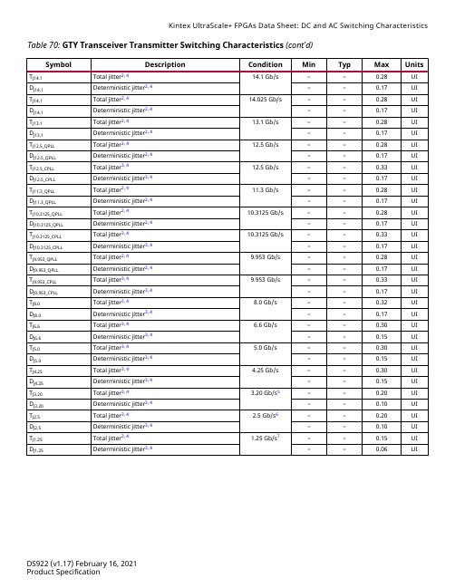
Table 70: GTY Transceiver Transmitter Switching Characteristics (cont'd)
Symbol
Condition
Modulated at 33 kHz
Bit rates ≤ 6.6 Gb/s Bit rates > 6.6 Gb/s and ≤ 8.0 Gb/s Bit rates > 8.0 Gb/s
32.75 Gb/s 28.21 Gb/s 16.375 Gb/s 15.0 Gb/s 14.1 Gb/s 13.1 Gb/s 12.5 Gb/s 11.3 Gb/s 10.32 Gb/s 10.32 Gb/s 9.953 Gb/s 9.953 Gb/s 8.0 Gb/s 6.6 Gb/s 5.0 Gb/s 4.25 Gb/s 3.2 Gb/s4 2.5 Gb/s5 1.25 Gb/s6 500 Mb/s7
Table 71: GTY Transceiver Receiver Switching Characteristics
Symbol
FGTYRX RXSST RXRL RXPPMTOL
Description
Serial data rate Receiver spread-spectrum tracking1 Run length (CID) Data/REFCLK PPM offset tolerance
Max
FGTYMAX 0
256 1250 700
Units
Gb/s ppm
UI ppm ppm
- 1、下载文档前请自行甄别文档内容的完整性,平台不提供额外的编辑、内容补充、找答案等附加服务。
- 2、"仅部分预览"的文档,不可在线预览部分如存在完整性等问题,可反馈申请退款(可完整预览的文档不适用该条件!)。
- 3、如文档侵犯您的权益,请联系客服反馈,我们会尽快为您处理(人工客服工作时间:9:00-18:30)。
Table 1-20: VITA 57.1 FMC HPC J35 Connections to FPGA U1 (Cont’d)
J35 FMC1 HPC Pin
Net Name
I/O
XCVX690T
Standard (U1) Pin
J35 FMC1 HPC Pin
Net Name
A38
FMC1_HPC_DP5_C2M_P
FPGA_DONE PWRCTL1_VCC4A_PG VCC12_P_IN PWRCTL_PWRGOOD LINEAR_POWER_GOOD
Color
GREEN/RED
GREEN GREEN GREEN GREEN GREEN
Description GREEN: FPGA initialization successful RED: FPGA initialization in progress or configuration CRC failure FPGA configured successfully FMC1 HPC power good 12V power ON TI power system power good DDR3 SODIMMs VTT power good
I2C Bus
PCA9548 USER_CLK_SDL/SCL FMC1_HPC_IIC_SDA/SCL NOT USED
I2C Switch Position
NA 0 1 2
Feature Descriptions
I2C Address 0b1110100 0b1011101 0bxxxxx00 NOT USED
Silicon Labs provides royalty-free Virtual COM Port (VCP) drivers for the host computer. These drivers permit the CP2103GM USB-to-UART bridge to appear as a COM port to communications application software (for example, TeraTerm or HyperTerm) that runs on the host computer. The VCP device drivers must be installed on the host PC prior to establishing communications with the VC709 board.
The USB Connector pin assignments and signal definitions between J17 and U44 are listed in Table 1-15.
Table 1-15: USB Connector J17 Pin Assignments and Signal Definitions
(1)
H4
B37
FMC1_HPC_DP6_C2M_N
A39
FMC1_HPC_DP5_C2M_N
(1)
H3
B40
NC
I/O Standard
XCVX690T (U1) Pin
(1)
G1
NA
C2
FMC1_HPC_DP0_C2M_P
(1)
E2
C3
FMC1_HPC_DP0_C2M_N
(1)
E1
C6
FMC1_HPC_DP0_M2C_P
4 D–
3 D_P
USB_D_P
Bidirectional differential serial data (P-side)
3 D+
4 GND
USB_UART_GND Signal ground
2 GND1 29 CNR_GND
Table 1-16 shows the USB connections between the FPGA and the UART.
LVCMOS18 AL32
D4
FMC1_HPC_GBTCLK0_M2C_P
(1)
G10
D5
FMC1_HPC_GBTCLK0_M2C_N
(1)
G9
D8
FMC1_HPC_LA01_CC_P
LVCMOS18
J40
D9
FMC1_HPC_LA01_CC_N
Chapter 1: VC709 Evaluation Board Features
USB-to-UART Bridge
[Figure 1-2, callout 13]
The VC709 board contains a Silicon Labs CP2103GM USB-to-UART bridge device (U44) which allows a connection to a host computer with a USB port. The USB cable is supplied in the VC709 evaluation kit (type-A end to host computer, type mini-B end to VC709 board connector J17). The CP2103GM is powered by the USB 5V provided by the host PC when the USB cable is plugged into the USB port on the VC709 board.
I/O Standard
XCVX690T (U1) Pin
NA
NA
(1)
N6
(1)
N5
(1)
P8
(1)
P7
(1)
E6
(1)
E5
(1)
F8
(1)
F7
(1)
E10
(1)
E9
(1)
M4
(1)
M3
VC709 Evaluation Board UG887 (v1.6) March 11, 2019
Chapter 1: VC709 Evaluation Board Features
TXD
Output
Refer to the Silicon Labs website for technical information on the CP2103GM and the VCP drivers.
VC709 Evaluation Board UG887 (v1.6) March 11, 2019
VC709 Evaluation Board UG887 (v1.6) March 11, 2019
Feature Descriptions
J35 FMC1 HPC Pin
A2 A3 A6 A7 A10 A11 A14 A15 A18 A19 A22 A23 A26
Net Name
FMC1_HPC_DP1_M2C_P FMC1_HPC_DP1_M2C_N FMC1_HPC_DP2_M2C_P FMC1_HPC_DP2_M2C_N FMC1_HPC_DP3_M2C_P FMC1_HPC_DP3_M2C_N FMC1_HPC_DP4_M2C_P FMC1_HPC_DP4_M2C_N FMC1_HPC_DP5_M2C_P FMC1_HPC_DP5_M2C_N FMC1_HPC_DP1_C2M_P FMC1_HPC_DP1_C2M_N FMC1_HPC_DP2_C2M_P
Table 1-16: FPGA to UART Connections
FPGA (U1)
Pin
Function Direction I/O Standard
Schematic Net Name
CP2103GM UART (U44)
Pin
Function Direction
AR34
RTS
Output
I/O
XCVX690T
Standard (U1) Pin
(1)
C6
(1)
C5
(1)
B8
(1)
B7
(1)
A6
(1)
A5
(1)
H8
(1)
H7
(1)
G6
(1)
G5
(1)
D4
(1)
D3
(1)
C2
J35 FMC1 HPC Pin
B1 B4 B5 B8 B9 B12 B13 B16 B17 B20 B21 B24 B25
C27
FMC1_HPC_LA27_N
LVCMOS18
H31
C30
FMC1_HPC_IIC_SCL
NA
U52.4
C31
FMC1_HPC_IIC_SDA
NA
U52.3
C34
GND
NA
NA
C35
VCC12_P
NA
NA
C37
VCC12_P
NA
NA
C39
VCC3V3
NA
NA
D1
PWRCTL1_VCC4B_PG
VC709 Evaluation Board UG887 (v1.6) March 11, 2019
Chapter 1: VC709 Evaluation Board Features
Reference Designator
Signal Name
DS1
FPGA_INIT_B
DS10 DS14 DS16 DS17 DS18
(1)
D8
C7
FMC1_HPC_DP0_M2C_N
(1)
D7
C10