98C-1 datasheet
ATE测量分析(输出功率)

X C = 9.810000
RC = 0.050000
零件均值 Parts Mean
XP
Total
9.771111 9.866667 9.866667 9.855556 9.744444 9.944444 9.933333 9.688889 9.788889 9.866667
87.940000 88.800000 88.800000 88.700000 87.700000 89.500000 89.400000 87.200000 88.100000 88.800000
10.00000 UCLx
均值图 mean chart
极差图 Range chart
UCLx pp 变差 0.326048 0.326048 0.326048 PV 0.326048 PV 基于公差base on parts spec LCLx 0.333333 0.000000 0.333333 TV #DIV/0! TV 19.14% #DIV/0! 19.14% #DIV/0! %EV 9.60000 基于零件变差base on parts variation 8.12% #DIV/0! 8.12% #DIV/0! B %AV 基于过程能力Base on process PP 20.79% #DIV/0! 20.79% #DIV/0! %RR 97.81% #DIV/0! 97.81% #DIV/0! %PV C A 公式A Formula 6.632894078 ndc 公式B Formula B 9.40000 X^2/nkr 8701.3200400 8701.3730867 8701.8670667 sumSQ(sum(men))/nr SUMSQ(sum(1-10part))/kr n=part k=men r=time 8702.0115333 8702.3346000 sumSQ(all) SUMSQ(sum(men-part))/r ANOVADF Table With SS Operator*Part Interaction ANOVA Table Interaction Source MS F P Source DF Without Operator*Part SS MS F P 0.4000 Parts 9 0.54703 0.06078 11.96733 0.00001 Parts 9 0.54703 0.06078 11.43800 0.00000 Operators 2 0.05305 0.02652 5.22227 0.01627 Operators 2 0.05305 0.02652 4.99128 0.00882 Operators*Part 18 0.09142 0.00508 0.94325 0.53317 C 0.3000Repeatability 60 0.32307 0.00538 Repeatability 78 0.41449 0.00531 Total 89 1.01456 Total 89 1.01456 UCLR Gauge R&R With Operator*Part Interaction Gauge R&R Without Operator*Part Interaction 0.2000 Source VarComp Stdev %Contribution %TV %Tolerance Source VarComp Stdev %Contribution %TV %Tolerance LCLR Total Gauge R&R 0.00610 0.07810 49.63% 70.45% 23.43% Total Gauge R&R 0.00602 0.07759 49.42% 70.30% 23.28% Repeatability 0.00538 0.07338 43.82% 66.19% 22.01% Repeatability 0.00531 0.07290 43.61% 66.04% 21.87% 0.00071 0.02674 5.82% 24.12% 8.02% Reproducibility 0.00071 0.02659 5.80% 24.09% 7.98% 0.1000 Reproducibility B Operator 0.00071 0.02674 5.82% 24.12% 8.02% Operator 0.00071 0.02659 5.80% 24.09% 7.98% Operators*Part 0.00000 0.00000 0.00% 0.00% 0.00% A Part - To - Part 0.00619 0.07867 50.37% 70.97% 23.60% Part - To - Part 0.00616 0.07850 50.58% 71.12% 23.55% 0.0000 Total Variation 0.01229 0.11085 100.00% 100.00% 33.26% Total Variation 0.01218 0.11038 100.00% 100.00% 33.11%
CS5341-CZZ;CS5341-DZZ;中文规格书,Datasheet资料
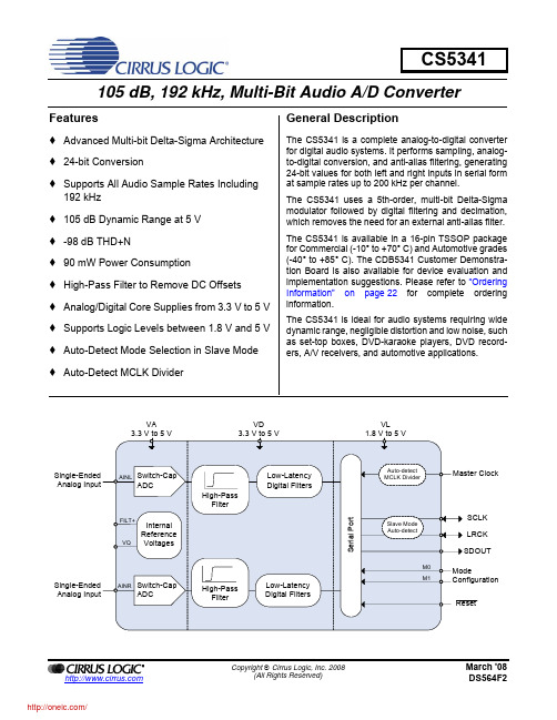
Single-Ended Analog Input
AINR Switch-Cap ADC
High-Pass Filter
Low-Latency Digital Filters
Serial Port
VL 1.8 V to 5 V
Auto-detect MCLK Divider
Master Clock
Slave Mode Auto-detect
The CS5341 is available in a 16-pin TSSOP package for Commercial (-10° to +70° C) and Automotive grades (-40° to +85° C). The CDB5341 Customer Demonstration Board is also available for device evaluation and implementation suggestions. Please refer to “Ordering Information” on page 22 for complete ordering information.
Confidential 05 dB, 192 kHz, Multi-Bit Audio A/D Converter
Features
Advanced Multi-bit Delta-Sigma Architecture 24-bit Conversion Supports All Audio Sample Rates Including
4.1 Single-, Double-, and Quad-Speed Modes ..................................................................................... 15 4.2 Operation as Either a Clock Master or Slave ................................................................................. 15
WKP101MCPEB0KR;WKP101MCPED0KR;WKP101MCPTG0KR;WKP101MCPSLRKR;WKP331MCPED0KR;中文规格书,Datasheet资料

Document Number: 22206For technical questions, contact: slcap@Revision: 08-Feb-101Ceramic AC CapacitorsClass X1, 760 V AC /Class Y1, 500 V ACWKPVishay DraloricNoteImpedance (Z) as a function of frequency (f) at T a = 20 °C (average).Measurement with lead length 6 mm.DESIGNDisc capacitors with epoxy coatingRATED VOLTAGE U R(X1):760 V AC , 50 Hz (IEC 60384-14.2)(Y1): 500 V AC , 50 Hz (IEC 60384-14.2)250 V AC , 60 Hz (UL1414, CSA C22.2)DIELECTRIC STRENGTH BETWEEN LEADSComponent test:4000 V AC , 50 Hz, 2 sAs repeated test admissible only once with: 3600 V AC , 50 Hz, 2 sRandom sampling test (destructive test):4000 V AC , 50 Hz, 60 sDIELECTRIC STRENGTH OF BODY INSULATION4000 V AC , 50 Hz, 60 s (destructive test)DISSIPATION FACTOR tan δ≤ 25 x 10-3INSULATION RESISTANCE R IS≥ 10 x 109 ΩCATEGORY TEMPERATURE RANGE ϑA(- 40 to + 125) °CCLIMATIC CATEGORY ACC. TO EN60068-140/125/21COATINGEpoxy dipped, insulating, flame retarding acc. to UL 94V-0TAPING AND SPECIAL LEAD CONFIGURATIONSOn requestMARKINGWKP 33 pF to 1.5 nFWKP 2.2 nF to 4.7 nFNote• All approval marks are also shown on the label.760 500 250 ~WKPVishay DraloricCeramic AC CapacitorsClass X1, 760 V AC /Class Y1, 500 V AC For technical questions, contact: slcap@Document Number: 222062Revision: 08-Feb-10Notes(1) Standard lead configuration, other lead spacing and diameter available on request.(2) Capacitance values from 470 pF to 4700 pF: The alternative usage of smaller VKP series is recommended for new application.ORDERING INFORMATION, CERAMIC X1/Y1 CAPACITORS WKPCAPACITANCE (2)(pF)TOL.(%) D x s (mm) F ± 1 (1)(mm) d ± 0.05 (1)(mm)V ± 0.5 (1)(mm)ORDERING CODECLASS 1N 75033± 10 , ± 20 8.0 x 6.012.50.6 1.9WKP330 CP KR CLASS 2K 120047± 10 , ± 20 8.0 x 6.012.50.6 2.3WKP470 CP KR68WKP680 CP KR CLASS 2K 1500100± 10 , ± 20 8.0 x 6.012.50.6 2.3WKP101 CP KR CLASS 2K 2000150± 10 , ± 20 8.0 x 6.012.50.6 2.3WKP151 CP KR220WKP221 CP KR CLASS 2K 4000330± 10 , ± 20 8.0 x 6.012.50.6 2.5WKP331 CP KR470WKP471 CP KR6809.0 x 6.0WKP681 CP KR 100010.0 x 6.00.8 2.7WKP102 CP KR150012.0 x 6.0WKP152 CPKR220013.0 x 6.0WKP222 CP KR330015.0 x 6.0WKP332 CP KR 390016.0 x 6.0WKP392 CP KR 470018.0 x 6.0WKP472 CP KR ORDERING CODE7th digit Capacitance Tolerance:± 10 % = K ± 20 % = M10th to 12th digit Lead Configuration (see General Information)R14th digitRoHS Compliant ComponentAPPROVALSIEC 60384 - 14 / 2nd Issue (1993) incl. Am. 1 (1995) - Safety Tests EN 132 400 (1994) - Safety TestsTHAT APPROVAL TOGETHER WITH THE CB TEST CERTIFICATE SUBSTITUTES THE NATIONAL APPROVAL OF THE FOLLOWING Belgium France Italy Austria China Japan Spain Denmark Greece Luxembourg Portugal Singapore Poland United Germany Ireland Netherlands Sweden Slovenia Hungaria Czech Republic Finland Iceland Norway Switzerland Korea IsraelY1 - Capacitor: CB-T est Certificate:X1 - Capacitor: CB-T est Certificate:DE-1-11002-A1DE-1-11002-A133 pF ... 4.7 nF 33 pF ... 4.7 nF500 V AC 760 V ACMinimum thickness of insulation: 0.4 mmUNDERWRITERS LABORATORIES INC.UL 1414Across-the-line, Antenna-coupling and Line-by-pass component.33 pF ... 4.7 nF250 V ACAgency Files / LicencesE 183 844 V1 S1CANADIAN STANDARDS ASSOCIATION CSA C22.2Across-the-line, antenna-coupling and line-by-pass component 33 pF ... 4.7 nF250 V ACNO 1-98Agency Files / LicencesE 183 844 V1 S1ORDERING INFORMATIONWKP 221M CP ED0K R SERIESCAP. VALUETOLERANCERATED VOLTAGELEADCONFIGURATIONINTERNAL CODEROHS COMPLIANTLegal Disclaimer Notice VishayDisclaimerALL PRODU CT, PRODU CT SPECIFICATIONS AND DATA ARE SU BJECT TO CHANGE WITHOU T NOTICE TO IMPROVE RELIABILITY, FUNCTION OR DESIGN OR OTHERWISE.Vishay Intertechnology, Inc., its affiliates, agents, and employees, and all persons acting on its or their behalf (collectively,“Vishay”), disclaim any and all liability for any errors, inaccuracies or incompleteness contained in any datasheet or in any other disclosure relating to any product.Vishay makes no warranty, representation or guarantee regarding the suitability of the products for any particular purpose or the continuing production of any product. To the maximum extent permitted by applicable law, Vishay disclaims (i) any and all liability arising out of the application or use of any product, (ii) any and all liability, including without limitation special, consequential or incidental damages, and (iii) any and all implied warranties, including warranties of fitness for particular purpose, non-infringement and merchantability.Statements regarding the suitability of products for certain types of applications are based on Vishay’s knowledge of typical requirements that are often placed on Vishay products in generic applications. Such statements are not binding statements about the suitability of products for a particular application. It is the customer’s responsibility to validate that a particular product with the properties described in the product specification is suitable for use in a particular application. Parameters provided in datasheets and/or specifications may vary in different applications and performance may vary over time. All operating parameters, including typical parameters, must be validated for each customer application by the customer’s technical experts. Product specifications do not expand or otherwise modify Vishay’s terms and conditions of purchase, including but not limited to the warranty expressed therein.Except as expressly indicated in writing, Vishay products are not designed for use in medical, life-saving, or life-sustaining applications or for any other application in which the failure of the Vishay product could result in personal injury or death. Customers using or selling Vishay products not expressly indicated for use in such applications do so at their own risk and agree to fully indemnify and hold Vishay and its distributors harmless from and against any and all claims, liabilities, expenses and damages arising or resulting in connection with such use or sale, including attorneys fees, even if such claim alleges that Vishay or its distributor was negligent regarding the design or manufacture of the part. Please contact authorized Vishay personnel to obtain written terms and conditions regarding products designed for such applications.No license, express or implied, by estoppel or otherwise, to any intellectual property rights is granted by this document or by any conduct of Vishay. Product names and markings noted herein may be trademarks of their respective owners.Material Category PolicyVishay Intertechnology, Inc. hereb y certifies that all its products that are identified as RoHS-Compliant fulfill the definitions and restrictions defined under Directive 2011/65/EU of The European Parliament and of the Council of June 8, 2011 on the restriction of the use of certain hazardous substances in electrical and electronic equipment (EEE) - recast, unless otherwise specified as non-compliant.Please note that some Vishay documentation may still make reference to RoHS Directive 2002/95/EC. We confirm that all the products identified as being compliant to Directive 2002/95/EC conform to Directive 2011/65/EU.Revision: 12-Mar-121Document Number: 91000分销商库存信息:VISHAY-BC-COMPONENTSWKP101MCPEB0KR WKP101MCPED0KR WKP101MCPTG0KR WKP101MCPSLRKR WKP331MCPED0KR WKP101MCPDF0KR WKP101MCPEF0KR WKP101MCPERUKR WKP101MCPQG0KR WKP151MCPDF0KR WKP151MCPEB0KR WKP151MCPEF0KR WKP151MCPERUKR WKP330MCPDF0KR WKP330MCPDRUKR WKP330MCPEF0KR WKP470MCPDF0KR WKP470MCPDRUKR WKP470MCPEF0KR WKP680MCPDF0KR WKP680MCPEF0KR WKP471MCPED0KR WKP221MCPDRUKR WKP221MCPED0KR WKP221MCPEF0KR WKP221MCPEFGKR WKP331MCPDF0KR WKP331MCPEF0KR WKP331MCPQG0KR WKP331MCPTE0KR WKP471MCPEF0KR WKP471MCPEFGKR WKP471MCPNZ0KR WKP471MCPSARKR WKP471MCPSVNKR WKP101KCPED0KR WKP101MCPERZKR WKP470MCPERZKR WKP681MCPDF0KR WKP681MCPEF0KR WKP681MCPEJ0KR WKP681MCPQG0KR WKP221MCPERUKR WKP221MCPERZKR WKP331MCPDRUKR WKP331MCPERUKR WKP331MCPERZKR WKP101KCPDF0KR WKP101KCPEF0KR WKP151KCPEF0KR WKP680KCPDF0KR WKP221KCPED0KR WKP221KCPERUKR WKP331KCPEF0KR WKP471MCPDF0KR WKP471MCPDRUKR WKP471MCPERUKR WKP102KCPED0KR WKP681MCPERUKR WKP681MCPERZKR WKP102MCPEH0KR WKP102MCPKX0KR WKP470KCPEF0KR WKP221KCPEF0KR WKP102MCPDF0KR WKP102MCPED0KR WKP102MCPEF0KR WKP102MCPEJ0KR WKP102MCPPA0KR WKP102MCPTH0KR WKP102MCPSAQKR WKP102MCPSUXKR WKP681KCPEJ0KR WKP102MCPDJ0KR WKP102MCPDRTKR WKP102MCPDRUKR WKP102MCPEJGKR WKP102MCPEJXKR WKP102MCPERTKR WKP102MCPERUKR WKP102MCPERYKR WKP102MCPRNAKR WKP102MCPSRKKR WKP152MCPEH0KR WKP152MCPEHNKR WKP152MCPQG0KR WKP152MCPTH0KR WKP102KCPEF0KR WKP152MCPEF0KR WKP152MCPEJ0KR WKP152MCPERUKR WKP152MCPERYKR WKP222MCPEH0KR WKP222MCPKX0KR WKP222MCPNV0KR WKP222MCPNZ0KR WKP222MCPQH0KR WKP222MCPTH0KR WKP222MCPSUXKR WKP222MCPDF0KR WKP222MCPDJ0KR WKP222MCPEF0KR WKP222MCPEJ0KR WKP222MCPEJGKR WKP222MCPEJXKR WKP222MCPSKQKR WKP222KCPQH0KR WKP222KCPEF0KR WKP102MCPERZKR WKP332MCPEH0KR WKP332MCPKX0KR WKP332MCPPK0KR WKP332MCPTH0KR WKP332MCPSLQKR WKP332MCPSUTKR WKP332MCPDF0KR WKP332MCPDJ0KR WKP332MCPEF0KR WKP332MCPEJ0KR WKP332MCPERUKR WKP332MCPSRKKR WKP472MCPDRUAR WKP472MCPERUAR。
89CV[1](高压传感器)
](https://img.taocdn.com/s3/m/5bc58e896529647d272852d4.png)
∙316L SS Pressure Sensor∙High Pressure∙0 - 100mV Output∙Absolute and Sealed GageDESCRIPTIONThe 89 constant voltage is a small profile, media compatible, piezoresistive silicon pressure sensor packaged in a 316L stainless steel housing. The 89 constant voltage features 5/16-32 UNEF threads and can be welded in place. It can also be packaged in a variety of threaded fittings such as 1/4 and 1/8NPT, 1/4BSP as well as custom process fittings. Contact factory for threaded fitting options.The 89 constant voltage is designed for high pressure OEM applications where compatibility with corrosive media is required. The sensing package utilizes silicon oil to transfer pressure from the 316L stainless steel diaphragm to the sensing element. For devices with leads, please see uncompensated datasheet. FEATURES APPLICATIONS∙Threaded Process Fittings or O-Ring Mount∙Hydraulic Controls∙-40ºC to +125ºC OperatingTemperature Range∙Process Control∙Pressure Calibrators∙±0.25% Pressure Non Linearity∙Refrigeration/Compressors∙Solid State ReliabilitySTANDARD RANGESRange psia psis0 to 1000 ∙∙0 to 3000 ∙∙0 to 5000 ∙∙89 Constant VoltageSeptember 20102/4PERFORMANCE SPECIFICATIONSAmbient Temperature: 25°C (unless otherwise specified)PARAMETERS MIN TYP MAX UNITS NOTESFull Scale Output Span 98 100 102 mV 1 Zero Pressure Output -1.0 1.0 mV Pressure Non Linearity-0.25 0.25 %Span 2Pressure Hysteresis ±0.05 %Span Input Resistance5500 9000 12500 ΩOutput Resistance 4000 6000 ΩTemperature Error – Span -1.0 1.0 %Span 3 Temperature Error – Zero -1.0 1.0 %Span 3 Thermal Hysteresis – Span ±0.05 %Span 3 Thermal Hysteresis – Zero ±0.05 %Span 3 Long Term Stability – Zero/Span ±0.1 %Span/yrSupply Voltage10 14 V Output Load Resistance 5 M Ω 4 Insulation Resistance (50Vdc) 50 M Ω 5Pressure Overload 3X Rated 6 Pressure Burst 4X Rated 7 Operating Temperature-40 +125 ºC 8 Compensated Temperature Range -20 +85 ºC 3 Storage Temperature -50+125ºC8 Media – Pressure PortLiquids and Gases compatible with 316/316L Stainless SteelNotes1. Calculated at FSP, 3000psi and 5000psi parts are tested at 2500psi.2. Best fit straight line between 0 and FSP.3. Over the compensated temperature range with respect to +25°C.4. Load resistance to reduce measurement errors due to output loading.5. Between case and sensing element.6. 3X or 10,000psi, whichever is less.7. The maximum pressure that can be applied to a transducer without rupture of either the sensing element or transducer. 8. Maximum temperature range for this product with standard cable and connector is -20°C to +105°C.The information in this sheet has been carefully reviewed and is believed to be accurate; however, no responsibility is assumed for inaccuracies. Furthermore, this information does not convey to the purchaser of such devices any license under the patent rights to the manufacturer. Measurement Specialties, Inc. reserves the right to make changes without further notice to any product herein. Measurement Specialties, Inc. makes no warranty, representation or guarantee regarding the suitability of its product for any particular purpose, nor does Measurement Specialties, Inc. assume any liability arising out of the application or use of any product or circuit and specifically disclaims any and all liability, including without limitation consequential or incidental damages. Typical parameters can and do vary in different applications. All operating parameters must be validated for each customer application by customer’s technical experts. Measurement Specialties, Inc. does not convey any license under its patent rights nor the rights of others.。
三极管型号及参数大全集
三极管s8050管脚图及参数---------------------------------------------------------------------------4 晶体管2SA1074参数 -----------------------------------------------------------------------------6 2SA1074---------------------------------------------------------------------------------------------6 晶体管2SA1068参数 -----------------------------------------------------------------------------8 2SA1068---------------------------------------------------------------------------------------------8 晶体管2SA107参数-------------------------------------------------------------------------------9 2SA107 ----------------------------------------------------------------------------------------------9 晶体管2SA1072A参数 ------------------------------------------------------------------------- 10 2SA1072A----------------------------------------------------------------------------------------- 10 2SA108 -------------------------------------------------------------------------------------------- 11 2SA1024------------------------------------------------------------------------------------------- 12 2SA1029------------------------------------------------------------------------------------------- 13 2SA1030------------------------------------------------------------------------------------------- 14 BC131 --------------------------------------------------------------------------------------------- 15 BC134 --------------------------------------------------------------------------------------------- 16 BC138 --------------------------------------------------------------------------------------------- 17 AUY35 -------------------------------------------------------------------------------------------- 18 AUY37 -------------------------------------------------------------------------------------------- 19 AUY36 -------------------------------------------------------------------------------------------- 20 AUY38 -------------------------------------------------------------------------------------------- 21 AUZ11 --------------------------------------------------------------------------------------------- 22 BC100 --------------------------------------------------------------------------------------------- 23 BC107 --------------------------------------------------------------------------------------------- 24 BC107P -------------------------------------------------------------------------------------------- 25 晶体管型号参数对照表 ------------------------------------------------------------------------- 26admin减小字体增大字体三极管s8050管脚图及参数、引脚实物图片[本站(中国单片机网),摘自/article/88/196/2008/2008012 37483.html]上一篇文章:三极管9013管脚参数封装说明、引脚实物图片下一篇文章:USB接口充电器电路图三极管s8050管脚图及参数作者:本站来源:本站原创发布时间:2008-1-23 9:43:22 [收藏] [评论]三极管s8050管脚图S8050 pdf,s8050 datasheet 8050参数,8050三极管参数资料pdf晶体管2SA1074参数整理日期:2008-8-31 20:27:34 资料编辑: 点击次数: 132SA1074材料:S外形:图集电极最大直流耗散功率Pcm_W:150集电极最大允许直流电流Icm_A:集电极_基极击穿电压BVcbo_V:集电极_基极击穿电压BVceo_V:160特征频率ft_Hz:放大倍数:国产管参考型号:此参数来自家电维修资料网整理日期:2008-8-31 20:27:47 资料编辑: 点击次数: 302SA1068材料:S外形:图集电极最大直流耗散功率Pcm_W:100集电极最大允许直流电流Icm_A:集电极_基极击穿电压BVcbo_V:集电极_基极击穿电压BVceo_V:150特征频率ft_Hz:40放大倍数:国产管参考型号:此参数来自家电维修资料网整理日期:2008-8-31 20:27:46 资料编辑: 点击次数: 172SA107材料:G外形:图集电极最大直流耗散功率Pcm_W:35m集电极最大允许直流电流Icm_A:-10m集电极_基极击穿电压BVcbo_V:-6集电极_基极击穿电压BVceo_V:特征频率ft_Hz:20000K放大倍数:国产管参考型号:3AG53A此参数来自家电维修资料网整理日期:2008-8-31 20:27:45 资料编辑: 点击次数: 162SA1072A材料:S外形:图集电极最大直流耗散功率Pcm_W:120集电极最大允许直流电流Icm_A:集电极_基极击穿电压BVcbo_V:集电极_基极击穿电压BVceo_V:120特征频率ft_Hz:放大倍数:国产管参考型号:此参数来自家电维修资料网整理日期:2008-8-31 20:27:33 资料编辑: 点击次数: 122SA108材料:G外形:图集电极最大直流耗散功率Pcm_W:80m集电极最大允许直流电流Icm_A:-10m集电极_基极击穿电压BVcbo_V:-20集电极_基极击穿电压BVceo_V:特征频率ft_Hz:45000K放大倍数:国产管参考型号:3AG54B此参数来自家电维修资料网材料:S外形:图集电极最大直流耗散功率Pcm_W:0.4 集电极最大允许直流电流Icm_A:0.1 集电极_基极击穿电压BVcbo_V:集电极_基极击穿电压BVceo_V:400 特征频率ft_Hz:放大倍数:国产管参考型号:3CK1E材料:S外形:图集电极最大直流耗散功率Pcm_W:0.2集电极最大允许直流电流Icm_A:0.1集电极_基极击穿电压BVcbo_V:30集电极_基极击穿电压BVceo_V:30特征频率ft_Hz:200放大倍数:100国产管参考型号:3CG120A此参数来自家电维修资料网材料:S外形:图集电极最大直流耗散功率Pcm_W:0.2集电极最大允许直流电流Icm_A:0.1集电极_基极击穿电压BVcbo_V:50集电极_基极击穿电压BVceo_V:55特征频率ft_Hz:200放大倍数:100国产管参考型号:3CG120B此参数来自家电维修资料网材料:S外形:图集电极最大直流耗散功率Pcm_W:135m 集电极最大允许直流电流Icm_A:100m 集电极_基极击穿电压BVcbo_V:20集电极_基极击穿电压BVceo_V:特征频率ft_Hz:300M放大倍数:国产管参考型号:3DG120D材料:S外形:图集电极最大直流耗散功率Pcm_W:200m 集电极最大允许直流电流Icm_A:集电极_基极击穿电压BVcbo_V:45集电极_基极击穿电压BVceo_V:特征频率ft_Hz:350M放大倍数:国产管参考型号:3DG110F材料:S外形:图集电极最大直流耗散功率Pcm_W:0.8 集电极最大允许直流电流Icm_A:集电极_基极击穿电压BVcbo_V:60 集电极_基极击穿电压BVceo_V:30 特征频率ft_Hz:40M放大倍数:100国产管参考型号:3DK14C材料:G外形:图集电极最大直流耗散功率Pcm_W:15 集电极最大允许直流电流Icm_A:-20 集电极_基极击穿电压BVcbo_V:-70 集电极_基极击穿电压BVceo_V:特征频率ft_Hz:2.5M放大倍数:国产管参考型号:3AD56BAUY37材料:G外形:图集电极最大直流耗散功率Pcm_W:30 集电极最大允许直流电流Icm_A:-10 集电极_基极击穿电压BVcbo_V:-100 集电极_基极击穿电压BVceo_V:特征频率ft_Hz:0.4M放大倍数:国产管参考型号:3AD56CAUY36材料:G外形:图集电极最大直流耗散功率Pcm_W:15 集电极最大允许直流电流Icm_A:-20 集电极_基极击穿电压BVcbo_V:-70 集电极_基极击穿电压BVceo_V:特征频率ft_Hz:3M放大倍数:国产管参考型号:3AD56B材料:G外形:图集电极最大直流耗散功率Pcm_W:30 集电极最大允许直流电流Icm_A:-10 集电极_基极击穿电压BVcbo_V:-130 集电极_基极击穿电压BVceo_V:特征频率ft_Hz:4M放大倍数:国产管参考型号:3AD56C材料:G外形:图集电极最大直流耗散功率Pcm_W:6 集电极最大允许直流电流Icm_A:-1 集电极_基极击穿电压BVcbo_V:-50 集电极_基极击穿电压BVceo_V:特征频率ft_Hz:3.5M放大倍数:国产管参考型号:3AD50A材料:S外形:图集电极最大直流耗散功率Pcm_W:0.59 集电极最大允许直流电流Icm_A:0.15 集电极_基极击穿电压BVcbo_V:350 集电极_基极击穿电压BVceo_V:300 特征频率ft_Hz:10M放大倍数:40国产管参考型号:3DG180N材料:S外形:图集电极最大直流耗散功率Pcm_W:260m 集电极最大允许直流电流Icm_A:100m 集电极_基极击穿电压BVcbo_V:50集电极_基极击穿电压BVceo_V:特征频率ft_Hz:150M放大倍数:国产管参考型号:3DG120D材料:S外形:图集电极最大直流耗散功率Pcm_W:0.3 集电极最大允许直流电流Icm_A:0.2 集电极_基极击穿电压BVcbo_V:集电极_基极击穿电压BVceo_V:50 特征频率ft_Hz:放大倍数:国产管参考型号:3DG120D晶体管型号参数对照表整理日期:2008-1-24 0:34:40 资料编辑: 点击次数: 9072晶体管型号反压Vbe0 电流Icm 功率Pcm 放大系数特征频率管子类型IRFU020 50V 15A 42W * * NMOS场效应IRFPG42 1000V 4A 150W * * NMOS场效应IRFPF40 900V 4.7A 150W * * NMOS场效应IRFP9240 200V 12A 150W * * PMOS场效应IRFP9140 100V 19A 150W * * PMOS场效应IRFP460 500V 20A 250W * * NMOS场效应IRFP450 500V 14A 180W * * NMOS场效应IRFP440 500V 8A 150W * * NMOS场效应IRFP353 350V 14A 180W * * NMOS场效应IRFP350 400V 16A 180W * * NMOS场效应IRFP340 400V 10A 150W * * NMOS场效应IRFP250 200V 33A 180W * * NMOS场效应IRFP240 200V 19A 150W * * NMOS场效应IRFP150 100V 40A 180W * * NMOS场效应晶体管型号反压Vbe0 电流Icm 功率Pcm 放大系数特征频率管子类型IRFP140 100V 30A 150W * * NMOS场效应IRFP054 60V 65A 180W * * NMOS场效应IRFI744 400V 4A 32W * * NMOS场效应IRFI730 400V 4A 32W * * NMOS场效应IRFD9120 100V 1A 1W * * NMOS场效应IRFD123 80V 1.1A 1W * * NMOS场效应本资料共207页,当前在第001页001002003004005006007008009010011012013014015016017018019020 021022023024025026027028029030 031032033034035036037038039040 041042043044045046047048049050 051052053054055056057058059060 061062063064065066067068069070 071072073074075076077078079080 081082083084085086087088089090 091092093094095096097098099100 101102103104105106107108109110 111112113114115116117118119120121122123124125126127128129130131132133134135136137138139140 141142143144145146147148149150 151152153154155156157158159160 161162163164165166167168169170 171172173174175176177178179180 181182183184185186187188189190 191192193194195196197198199200 201202203204205206207三极管型号查询时间:2008-12-24 19:00:32 作者:无被阅:上一篇文章:三极管资料大全下一篇文章:三极管型号查询三极管资料大全时间:2008-12-24 19:04:35 作者:无被阅:下一篇文章:三极管参数大全三极管资料大全时间:2008-12-24 19:04:35 作者:无被阅:。
89C52_datasheet
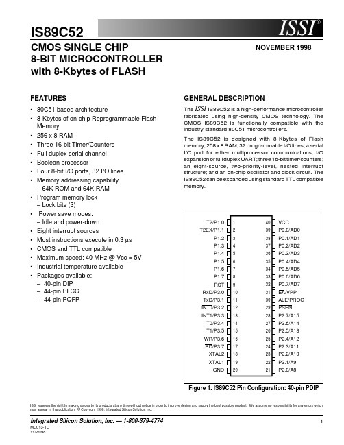
ISSI reserves the right to make changes to its products at any time without notice in order to improve design and supply the best possible product. We assume no responsibility for any errors which may appear in this publication. © Copyright 1998, Integrated Silicon Solution, Inc.8-BIT MICROCONTROLLER with 8-Kbytes of FLASHFEATURES•80C51 based architecture•8-Kbytes of on-chip Reprogrammable Flash Memory•256 x 8 RAM•Three 16-bit Timer/Counters •Full duplex serial channel •Boolean processor•Four 8-bit I/O ports, 32 I/O lines •Memory addressing capability – 64K ROM and 64K RAM •Program memory lock – Lock bits (3)• Power save modes:– Idle and power-down •Eight interrupt sources•Most instructions execute in 0.3 µs •CMOS and TTL compatible•Maximum speed: 40 MHz @ Vcc = 5V •Industrial temperature available •Packages available:– 40-pin DIP – 44-pin PLCC – 44-pin PQFPGENERAL DESCRIPTIONThe ISSI IS89C52 is a high-performance microcontroller fabricated using high-density CMOS technology. The CMOS IS89C52 is functionally compatible with the industry standard 80C51 microcontrollers.The IS89C52 is designed with 8-Kbytes of Flash memory, 258 x 8 RAM; 32 programmable I/O lines; a serial I/O port for either multiprocessor communications, I/O expansion or full duplex UART; three 16-bit timer/counters;an eight-source, two-priority-level, nested interrupt structure; and an on-chip oscillator and clock circuit. The IS89C52 can be expanded using standard TTL compatible memory.Figure 1. IS89C52 Pin Configuration: 40-pin PDIP12345678910111213141516171819204039383736353433323130292827262524232221T2/P1.0T2EX/P1.1P1.2P1.3P1.4P1.5P1.6P1.7RST RxD/P3.0TxD/P3.1INT0/P3.2INT1/P3.3T0/P3.4T1/P3.5WR/P3.6RD/P3.7XTAL2XTAL1GNDVCC P0.0/AD0P0.1/AD1P0.2/AD2P0.3/AD3P0.4/AD4P0.5/AD5P0.6/AD6P0.7/AD7EA/VPP ALE/PROG PSEN P2.7/A15P2.6/A14P2.5/A13P2.4/A12P2.3/A11P2.2/A10P2.1/A9P2.0/A8IS89C52Figure 2. IS89C52 Pin Configuration: 44-pin PLCC2Integrated Silicon Solution, Inc. — 1-800-379-4774MC013-1CIS89C52Figure 3. IS89C52 Pin Configuration: 44-pin PQFPIS89C52Figure 4. IS89C52 Block Diagram4Integrated Silicon Solution, Inc. — 1-800-379-4774MC013-1CIS89C52Table 1. Detailed Pin DescriptionSymbol PDIP PLCC PQFP I/O Name and FunctionALE/PROG303327I/O Address Latch Enable: Output pulse for latching the low byteof the address during an address to the external memory. Innormal operation, ALE is emitted at a constant rate of 1/6 theoscillator frequency, and can be used for external timing orclocking. Note that one ALE pulse is skipped during eachaccess to external data memory. This pin is also the ProgramPulse input (PROG) during Flash programming.EA/V PP313529I External Access enable:EA must be externally held low toenable the device to fetch code from external program memorylocations 0000H to FFFFH. If EA is held high, the deviceexecutes from internal program memory unless the programcounter contains an address greater than 0FFFH. This alsoreceives the 12V programming enable voltage (V PP) duringFlash programming.P0.0-P0.739-3243-3637-30I/O Port 0: Port 0 is an 8-bit open-drain, bidirectional I/O port. Port0 pins that have 1s written to them float and can be used as high-impedance inputs. Port 0 is also the multiplexed low-orderaddress and data bus during accesses to external program anddata memory. In this application, it uses strong internal pullupswhen emitting 1s.Port 0 also receives the code bytes during programmablememory programming and outputs the code bytes duringprogram verification. External pullups are required during pro-gram verification.P1.0-P1.71-82-940-44I/O Port 1: Port 1 is an 8-bit bidirectional I/O port with internal1-3pullups. Port 1 pins that have 1s written to them are pulled highby the internal pullups and can be used as inputs. As inputs,Port 1 pins that are externally pulled low will source currentbecause of the internal pullups. (See DC Characteristics: I IL).The Port 1 output buffers can sink/source four TTL inputs.Port 1 also receives the low-order address byte during Flashprogramming and verification.1240I T2(P1.0): Timer/Counter 2 external count input.2341I T2EX(P1.1): Timer/Counter 2 trigger input.P2.0-P2.721-2824-3118-25I/O Port 2: Port 2 is an 8-bit bidirectional I/O port with internalpullups. Port 2 pins that have 1s written to them are pulled highby the internal pullups and can be used as inputs. As inputs,Port 2 pins that are externally pulled low will source currentbecause of the internal pullups. (See DC Characteristics: I IL).Port 2 emits the high order address byte during fetches fromexternal program memory and during accesses to external datamemory that used 16-bit addresses (MOVX @ DPTR). In thisapplication, Port 2uses strong internal pullups when emitting1s. During accesses to external data memory that use 8-bitaddresses (MOVX @ Ri [i = 0, 1]), Port 2 emits the contents ofthe P2 Special Function Register.Port 2 also receives the high-order bits and some controlsignals during Flash programming and verification. P2.6 andP2.7 are the control signals while the chip programs anderases.IS89C526Integrated Silicon Solution, Inc. — 1-800-379-4774MC013-1CSymbol PDIP PLCC PQFP I/O Name and FunctionP3.0-P3.710-1711, 13-195, 7-13I/OPort 3: Port 3 is an 8-bit bidirectional I/O port with internal pullups. Port 3 pins that have 1s written to them are pulled high by the internal pullups and can be used as inputs. As inputs,Port 3 pins that are externally pulled low will source current because of the internal pullups. (See DC Characteristics: I IL ).Port 3 also serves the special features of the IS89C52, as listed below:10115I RxD (P3.0): Serial input port.11137O TxD (P3.1): Serial output port.12148I INT0 (P3.2): External interrupt 0.13159I INT1 (P3.3): External interrupt 1.141610I T0 (P3.4): Timer 0 external input.151711I T1 (P3.5): Timer 1 external input.161812O WR (P3.6): External data memory write strobe.171913O RD (P3.7): External data memory read strobe.PSEN293226OProgram Store Enable: The read strobe to external program memory. When the device is executing code from the external program memory, PSEN is activated twice each machine cycle except that two PSEN activations are skipped during each access to external data memory. PSEN is not activated during fetches from internal program memory.RST 9104IReset: A high on this pin for two machine cycles while the oscillator is running, resets the device. An internal MOS resistor to GND permits a power-on reset using only an external capacitor connected to Vcc.XTAL 1192115I Crystal 1: Input to the inverting oscillator amplifier and input to the internal clock generator circuits.XTAL 2182014O Crystal 2: Output from the inverting oscillator amplifier.GND 202216I Ground: 0V reference.Vcc404438IPower Supply: This is the power supply voltage for operation.Table 1. Detailed Pin Description (continued)IS89C52OPERATING DESCRIPTIONThe detail description of the IS89C52 included in this description are:• Memory Map and Registers• Timer/Counters• Serial Interface• Interrupt System• Other Information• Flash MemoryMEMORY MAP AND REGISTERSMemoryThe IS89C52 has separate address spaces for program and data memory. The program and data memory can be up to 64K bytes long. The lower 8K program memory can reside on-chip. Figure 5 shows a map of the IS89C52 program and data memory.The IS89C52 has 256 bytes of on-chip RAM, plus numbers of special function registers. The lower 128 bytes can be accessed either by direct addressing or by indirect addressing. Figure 6 shows internal data memory organization and SFR Memory Map.The lower 128 bytes of RAM can be divided into three segments as listed below and shown in Figure 7.1.Register Banks 0-3: locations 00H through 1FH (32bytes). The device after reset defaults to register bank0. To use the other register banks, the user must selectthem in software. Each register bank contains eight 1-byte registers R0-R7. Reset initializes the stack point to location 07H, and is incremented once to start from 08H, which is the first register of the second register bank.2.Bit Addressable Area: 16 bytes have been assignedfor this segment 20H-2FH. Each one of the 128 bits of this segment can be directly addressed (0-7FH). Each of the 16 bytes in this segment can also be addressed as a byte.3.Scratch Pad Area: 30H-7FH are available to the useras data RAM. However, if the data pointer has been initialized to this area, enough bytes should be left aside to prevent SP data destruction.Figure 5. IS89C52 Program and Data Memory StructureIS89C528Integrated Silicon Solution, Inc. — 1-800-379-4774MC013-1CSPECIAL FUNCTION REGISTERSThe Special Function Registers (SFR's) are located in upper 128 Bytes direct addressing area. The SFR Memory Map in Figure 6 shows that.Not all of the addresses are occupied. Unoccupied addresses are not implemented on the chip. Read accesses to these addresses in general return random data, and write accesses have no effect.User software should not write 1s to these unimplemented locations, since they may be used in future microcontrollers to invoke new features. In that case, the reset or inactive values of the new bits will always be 0, and their active values will be 1.The functions of the SFRs are outlined in the following sections, and detailed in Table 2.Accumulator (ACC)ACC is the Accumulator register. The mnemonics for Accumulator-specific instructions, however, refer to the Accumulator simply as A.B Register (B)The B register is used during multiply and divide operations.For other instructions it can be treated as another scratch pad register.Program Status Word (PSW). The PSW register contains program status information.Figure 6. Internal Data Memory and SFR Memory MapFigure 7. Lower 128 Bytes of Internal RAMIS89C52SPECIAL FUNCTION REGISTERS (Continued)Stack Pointer (SP)The Stack Pointer Register is eight bits wide. It is incremented before data is stored during PUSH and CALL executions. While the stack may reside anywhere in on-chip RAM, the Stack Pointer is initialized to 07H after a reset. This causes the stack to begin at location 08H. Data Pointer (DPTR)The Data Pointer consists of a high byte (DPH) and a low byte (DPL). Its function is to hold a 16-bit address. It may be manipulated as a 16-bit register or as two independent 8-bit registers.Ports 0 To 3P0, P1, P2, and P3 are the SFR latches of Ports 0, 1, 2, and 3, respectively.Serial Data Buffer (SBUF)The Serial Data Buffer is actually two separate registers, a transmit buffer and a receive buffer register. When data is moved to SBUF, it goes to the transmit buffer, where it is held for serial transmission. (Moving a byte to SBUF initiates the transmission.) When data is moved from SBUF, it comes from the receive buffer.Timer RegistersRegister pairs (TH0, TL0) and (TH1, TL1) are the 16-bit Counter registers for Timer/Counters 0 and 1, respectively. Capture RegistersThe register pair (RCAP2H, RCAP2L) are the Capture registers for the Timer 2 Capture Mode. In this mode, in response to a transition at the IS89C52's T2EX pin, TH2 and TL2 are copied into RCAP2H and RCAP2L. Timer 2 also has a 16-bit auto-reload mode, and RCAP2H and RCAP2L hold the reload value for this mode.Control RegistersSpecial Function Registers IP, IE, TMOD, TCON, SCON, and PCON contain control and status bits for the interrupt system, the Timer/Counters, and the serial port. They are described in later sections of this chapter.IS89C52Table 2. Special Function RegistersSymbol Description Direct Address Bit Address, Symbol, or Alternative Port Function Reset Value ACC(1)Accumulator E0H E7E6E5E4E3E2E1E000H B(1) B register F0H F7F6F5F4F3F2F1F000H DPH Data pointer (DPTR) high83H00H DPL Data pointer (DPTR) low82H00HAF AE AD AC AB AA A9A8 IE(1)Interrupt enable A8H EA——ES ET1EX1ET0EX00XX00000BBF BE BD BC BB BA B9B8 IP(1)Interrupt priority B8H———PS PT1PX1PT0PX0XXX00000B8786858483828180 P0(1)Port 080H P0.7P0.6P0.5P0.4P0.3P0.2P0.1P0.0FFHAD7AD6AD5AD4AD3AD2AD1AD09796959493929190 P1(1)Port 190H P1.7P1.6P1.5P1.4P1.3P1.2P1.1P1.0FFHA7A6A5A4A3A2A1A0 P2(1)Port 2A0H P2.7P2.6P2.5P2.4P2.3P2.2P2.1P2.0FFHAD15AD14AD13AD12AD11AD10AD9AD8B7B6B5B4B3B2B1B0 P3(1)Port 3B0H P3.7P3.6P3.5P3.4P3.3P3.2P3.1P3.0FFHRD WR T1T0INT1INT0TXD RXD PCON Power control87H SMOD———GF1GF0PD IDL0XXX0000BD7D6D5D4D3D2D1D0 PSW(1)Program status word D0H CY AC F0RS1RS0OV—P00H SBUF Serial data buffer99H XXXXXXXXB9F9E9D9C9B9A9998 SCON(1)Serial controller98H SM0SM1SM2REN TB8RB8TI RI00H SP Stack pointer81H07H8F8E8D8C8B8A8988 TCON(1)Timer control88H TF1TR1TF0TR0IE1IT1IE0IT000H TMOD Timer mode89H GATE C/T M1M0GATE C/T M1M000H TH0Timer high 08CH00H TH1Timer high 18DH00H TL0Timer low 08AH00H TL1Timer low 18BH00H RCAP2H(2)Capture high CAH00H RCAP2L(2)Capture low CBH00H TL2(2)Timer low 2CCH00H Notes:1. Denotes bit addressable.2. SFRs are added to the 80C51 SFRs.10Integrated Silicon Solution, Inc. — 1-800-379-4774MC013-1CThe detail description of each bit is as follows:PSW:Program Status Word. Bit Addressable.76543210CY AC F0RS1RS0OV—P Register Description:CY PSW.7Carry flag.AC PSW.6Auxiliary carry flag.F0PSW.5Flag 0 available to the user for g e n e r a lpurpose.RS1PSW.4Register bank selector bit 1.(1)RS0PSW.3Register bank selector bit 0.(1)OV PSW.2Overflow flag.—PSW.1Usable as a general purpose flagP PSW.0Parity flag. Set/Clear by hardware eachinstruction cycle to indicate an odd/evennumber of “1” bits in the accumulator.Note:1.The value presented by RS0 and RS1 selects the corre-sponding register bank.RS1RS0Register Bank Address00000H-07H01108H-0FH10210H-17H11318H-1FH PCON:Power Control Register. Not Bit Addressable. 76543210 SMOD———GF1GF0PD IDL Register Description:SMOD Double baud rate bit. If Timer 1 is used to generate baud rate and SMOD=1, the baud rate is doubledwhen the serial port is used in modes 1, 2, or 3.—Not implemented, reserve for future use.(1)—Not implemented, reserve for future use.(1)—Not implemented, reserve for future use.(1)GF1General purpose flag bit.GF0General purpose flag bit.PD Power-down bit. Setting this bit activates power-down mode.IDL Idle mode bit. Setting this bit activates idle mode.If 1s are written to PD and IDL at the same time,PD takes precedence.Note:1. User software should not write 1s to reserved bits. Thesebits may be used in future products to invoke new features.IE:Interrupt Enable Register. Bit Addressable. 76543210 EA——ES ET1EX1ET0EX0 Register Description:EA IE.7Disable all interrupts. If EA=0, nointerrupt will be acknowledged. If EA=1,each interrupt source is individuallyenabled or disabled by setting orclearing its enable bit.—IE.6Not implemented, reserve for futureuse.(5)—IE.5Not implemented, reserve for futureuse.(5)ES IE.4Enable or disable the serial portinterrupt.ET1IE.3Enable or disable the Timer 1 overflowinterrupt.EX1IE.2Enable or disable External Interrupt 1. ET0IE.1Enable or disable the Timer 0 overflowinterrupt.EX0IE.0Enable or disable External Interrupt 0.Note: To use any of the interrupts in the 80C51 Family, the following three steps must be taken:1. Set the EA (enable all) bit in the IE register to 1.2. Set the coresponding individual interrupt enable bit inthe IE register to 1.3. Begin the interrupt service routine at the correspondingVector Address of that interrupt (see below).Interrupt Source Vector AddressIE00003HTF0000BHIE10013HTF1001BHRI & TI0023H4. In addition, for external interrupts, pins INT0 and INT1(P3.2 and P3.3) must be set to 1, and depending onwhether the interrupt is to be level or transition acti-vated, bits IT0 or IT1 in the TCON register may need tobe set to 0 or 1.ITX = 0 level activated (X = 0, 1)ITX = 1 transition activateder software should not write 1s to reserved bits. Thesebits may be used in future products to invoke newfeatures.IP:Interrupt Priority Register. Bit Addressable. 76543210———PS PT1PX1PT0PX0 Register Description:—IP.7Not implemented, reserve for future use(3)—IP.6Not implemented, reserve for future use(3)—IP.5Not implemented, reserve for future use(3) PS IP.4Defines Serial Port interrupt priority level PT1IP.3Defines Timer 1 interrupt priority level PX1IP.2Defines External Interrupt 1 priority level PT0IP.1Defines Timer 0 interrupt priority level PX0IP.0Defines External Interrupt 0 priority level Notes:1.In order to assign higher priority to an interrupt thecoresponding bit in the IP register must be set to 1. Whilean interrupt service is in progress, it cannot be interrupted by a lower or same level interrupt.2.Priority within level is only to resolve simultaneousrequests of the same priority level. From high-to-low,interrupt sources are listed below:IE0TF0IE1TF1RI or TITF2 or EXF2er software should not write 1s to reserved bits. Thesebits may be used in future products to invoke new features.TCON:Timer/Counter Control Register. Bit Addressable 76543210TF1TR1TF0TR0IE1IT1IE0IT0 Register Description:TF1TCON.7Timer 1 overflow flag. Set by hardwarewhen the Timer/Counter 1 overflows.Cleared by hardware as processorvectors to the interrupt service routine. TR1TCON.6Timer 1 run control bit. Set/Cleared bysoftware to turn Timer/Counter 1 ON/OFF.TF0TCON.5Timer 0 overflow flag. Set by hardwarewhen the Timer/Counter 0 overflows.Cleared by hardware as processorvectors to the interrupt service routine. TR0TCON.4Timer 0 run control bit. Set/Cleared bysoftware to turn Timer/Counter 0 ON/OFF.IE1TCON.3External Interrupt 1 edge flag. Set byhardware when the External Interruptedge is detected. Cleared by hardwarewhen interrupt is processed.IT1TCON.2Interrupt 1 type control bit. Set/Clearedby software specify falling edge/low leveltriggered External Interrupt.IE0TCON.1External Interrupt 0 edge flag. Set byhardware when the External Interruptedge is detected. Cleared by hardwarewhen interrupt is processed.IT0TCON.0Interrupt 0 type control bit. Set/Clearedby software specify falling edge/low leveltriggered External Interrupt.12Integrated Silicon Solution, Inc. — 1-800-379-4774MC013-1CTMOD:Timer/Counter Mode Control Register.Not Bit Addressable.Timer 1 Timer 0GATE C/T M1M0GATE C/T M1M0 GATE When TRx (in TCON) is set and GATE=1, TIMER/ COUNTERx will run only while INTx pin is high(hardware control). When GATE=0, TIMER/COUNTERx will run only while TRx=1 (softwarecontrol).C/T Timer or Counter selector. Cleared for Timer operation (input from internal system clock). Setfor Counter operation (input from Tx input pin). M1Mode selector bit.(1)M0Mode selector bit.(1)Note 1:M1M0Operating Mode00Mode 0. (13-bit Timer)01Mode 1. (16-bit Timer/Counter)10Mode 2. (8-bit auto-load Timer/Counter)11Mode 3. (Splits Timer 0 into TL0 andTH0. TL0 is an 8-bit Timer/Countercontroller by the standard Timer 0control bits. TH0 is an 8-bit Timer andis controlled by Timer 1 control bits.) 11Mode 3. (Timer/Counter 1 stopped).SCON:Serial Port Control Register. Bit Addressable. 76543210 SM0SM1SM2REN TB8RB8TI RI Register Description:SM0SCON.7Serial port mode specifier.(1)SM1SCON.6Serial port mode specifier.(1)SM2SCON.5Enable the multiprocessor com-munication feature in mode 2 and 3. Inmode 2 or 3, if SM2 is set to 1 then RIwill not be activated if the received 9thdata bit (RB8) is 0. In mode 1, if SM2=1then RI will not be activated if valid stopbit was not received. In mode 0, SM2should be 0.REN SCON.4Set/Cleared by software to Enable/Disable reception.TB8SCON.3The 9th bit that will be transmitted inmode 2 and 3. Set/Cleared by software. RB8SCON.2In modes 2 and 3, RB8 is the 9th databit that was received. In mode 1, ifSM2=0, RB8 is the stop bit that wasreceived. In mode 0, RB8 is not used. TI SCON.1Transmit interrupt flag. Set by hardwareat the end of the eighth bit time in mode0, or at the beginning of the stop bit inthe other modes. Must be cleared bysoftware.RI SCON.0Receive interrupt flag. Set by hardwareat the end of the eighth bit time in mode0, or halfway through the stop bit timein the other modes (except see SM2).Must be cleared by software.Note 1:SM0SM1MODE Description Baud Rate000Shift register Fosc/120118-bit UART Variable1029-bit UART Fosc/64 orFosc/321139-bit UART VariableT2CON:Timer/Counter 2 Control Register. Bit Addressable. 76543210 TF2EXF2RCLK TCLK EXEN2TR2C/T2CP/RL2 Register Description:TF2T2CON.7Timer 2 overflow flag set by hardwareand cleared by software. TF2 cannotbe set when either RCLK = 1 orTCLK = 1.EXF2T2CON.6Timer 2 external flag set when either acapture or reload is caused by anegative transition on T2EX, andEXEN2 = 1. When Timer 2 interrupt isenabled, EXF2 = 1 causes the CPU tovector to the Timer 2 interrupt routine.EXF2 must be cleared by software. RCLK T2CON.5Receive clock flag. When set, causesthe Serial Port to use Timer 2 overflowpulses for its receive clock in modes 1and 3. RCLK = 0 causes Timer 1overflow to be used for the receiveclock.TLCK T2CON.4Transmit clock flag. When set, causesthe Serial Port to use Timer 2 overflowpulses for its transmit clock in modes 1and 3. TCLK = 0 causes Timer 1overflows to be used for the transmitclock.EXEN2T2CON.3 Timer 2 external enable flag.When set, allows a capture or reload tooccur as a result of negative transitionon T2EX if Timer 2 is not being used toclock the Serial Port, EXEN2 = 0 causesTimer 2 to ignore events at T2EX.TR2T2CON.2Software START/STOP control forTimer 2. A logic 1 starts the Timer.C/T2T2CON.1Timer or Counter select.0 = Internal Timer. 1 = External EventCounter (triggered by falling edge). CP/RL2T2CON.0Capture/Reload flag.When set, captures occur on negativetransitions at T2EX if EXEN2 = 1. Whencleared, auto-reloads occur either withTimer 2 overflows or negativetransitions at T2EX when EXEN2 = 1.When either RCLK = 1 or TCLK = 1,this bit is ignored and the Timer isforced to auto-reload on Timer 2overflow.Note:1. Timer 2 Operating ModesRCLK + TCLK CP/RL2TR2MODE00116-Bit Auto-Reload01116-Bit Capture1X1Baud Rate GeneratorX X0(Off)14Integrated Silicon Solution, Inc. — 1-800-379-4774MC013-1CTIMER/COUNTERSThe IS89C52 has two 16-bit Timer/Counter registers: Timer 0 and Timer 1. All two can be configured to operate either as Timers or event Counters.As a Timer, the register is incremented every machine cycle. Thus, the register counts machine cycles. Since a machine cycle consists of 12 oscillator periods, the count rate is 1/12 of the oscillator frequency.As a Counter, the register is incremented in response to a 1-to-0 transition at its corresponding external input pin, T0 and T1. The external input is sampled during S5P2 of every machine cycle. When the samples show a high in one cycle and a low in the next cycle, the count is incremented. The new count value appears in the register during S3P1 of the cycle following the one in which the transition was detected. Since two machine cycles (24 oscillator periods) are required to recognize a 1-to-0 transition, the maximum count rate is 1/24 of the oscillator frequency. There are no restrictions on the duty cycle of the external input signal, but it should be held for at least one full machine cycle to ensure that a given level is sampled at least once before it changes.In addition to the Timer or Counter functions, Timer 0 and Timer 1 have four operating modes: 13-bit timer, 16-bit timer, 8-bit auto-reload, split timer. Timer 2 in the IS89C52 has three modes of operation: Capture, Auto-Reoload, and Baud Rate Generator.Timer 0 and Timer 1The Timer or Counter function is selected by control bitsC/T in the Special Function Regiser TMOD. These twoTimer/Counters have four operating modes, which areselected by bit pairs (M1, M0) in TMOD. Modes 0, 1, and 2are the same for both Timer/Counters, but Mode 3 is different.The four modes are described in the following sections. Mode 0:Both Timers in Mode 0 are 8-bit Counters with a divide-by-32prescaler. Figure 8 shows the Mode 0 operation as it appliesto Timer 1.In this mode, the Timer register is configured as a 13-bitregister. As the count rolls over from all 1s to all 0s, it sets theTimer interrupt flag TF1. The counted input is enabled to theTimer when TR1 = 1 and either GATE = 0 or INT1 = 1. SettingGATE = 1 allows the Timer to be controlled by external input INT1, to facilitate pulse width measurements. TR1 is a control bit in the Special Function Register TCON. Gate is inTMOD.The 13-bit register consists of all eight bits of TH1 and thelower five bits of TL1. The upper three bits of TL1 areindeterminate and should be ignored. Setting the run flag(TR1) does not clear the registers.Mode 0 operation is the same for Timer 0 as for Timer 1,except that TR0, TF0 and INT0 replace the correspondingTimer 1 signals in Figure 8. There are two different GATEbits, one for Timer 1 (TMOD.7) and one for Timer 0 (TMOD.3).Figure 8. Timer/Counter 1 Mode 0: 13-Bit Counter16Integrated Silicon Solution, Inc. — 1-800-379-4774MC013-1CMode 1:Mode 1 is the same as Mode 0, except that the Timer register is run with all 16 bits. The clock is applied to the combined high and low timer registers (TL1/TH1). As clock pulses are received, the timer counts up: 0000H, 0001H,0002H, etc. An overflow occurs on the FFFFH-to-0000H overflow flag. The timer continues to count. The overflow flag is the TF1 bit in TCON that is read or written by software (see Figure 9).Mode 2:Mode 2 configures the Timer register as an 8-bit Counter (TL1) with automatic reload, as shown in Figure 10. Overflow from TL1 not only sets TF1, but also reloads TL1 with the contents of TH1, which is preset by software. The reload leaves the TH1 unchanged. Mode 2 operation is the same for Timer/Counter 0.Mode 3:Timer 1 in Mode 3 simply holds its count. The effect is the same as setting TR1 = 0. Timer 0 in Mode 3 establishes TL0and TH0 as two separate counters. The logic for Mode 3 on Timer 0 is shown in Figure 11. TL0 uses the Timer 0 control bits: C/T , GATE, TR0, INT0, and TF0. TH0 is locked into a timer function (counting machine cycles) and over the use of TR1 and TF1 from Timer 1. Thus, TH0 now controls the Timer 1 interrupt.Mode 3 is for applications requiring an extra 8-bit timer or counter. With Timer 0 in Mode 3, the IS89C52 can appear to have four Timer/Counters. When Timer 0 is in Mode 3,Timer 1 can be turned on and off by switching it out of and into its own Mode 3. In this case, Timer 1 can still be used by the serial port as a baud rate generator or in any application not requiring an interrupt.Figure 10. Timer/Counter 1 Mode 2: 8-Bit Auto-ReloadFigure 9. Timer/Counter 1 Mode 1: 16-Bit Counter。
X9C103_DataSheet

1©Xicor, Inc. 1994, 1995 Patents PendingCharacteristics subject to change without notice3863-2.4 9/18/96 T2/C0/D0 SH DESCRIPTIONThe Xicor X9C102/103/104/503 is a solid state nonvola-tile potentiometer and is ideal for digitally controlledresistance trimming.The X9C102/103/104/503 is a resistor array composed of99 resistive elements. Between each element and at either end are tap points accessible to the wiper element.The position of the wiper element is controlled by the CS ,U/D , and INC inputs. The position of the wiper can bestored in nonvolatile memory and then be recalled upon asubsequent power-up operation.The resolution of the X9C102/103/104/503 is equal tothe maximum resistance value divided by 99. As anexample, for the X9C503 (50K Ω) each tap point repre-sents 505Ω.All Xicor nonvolatile memories are designed and testedfor applications requiring extended endurance and dataretention.FEATURES •Compatible with X9102/103/104/503•Low Power CMOS —V CC = 5V —Active Current, 3mA Max —Standby Current, 500µA Max •99 Resistive Elements —Temperature Compensated —± 20% End to End Resistance Range •100 Wiper Tap Points —Wiper Positioned via Three-Wire Interface —Similar to TTL Up/Down Counter —Wiper Position Stored in Nonvolatile Memory and Recalled on Power-Up •100 Year Wiper Position Data Retention •X9C102 = 1K Ω•X9C103 = 10K Ω•X9C503 = 50K Ω•X9C104 = 100K ΩE 2POT ™ Nonvolatile Digital PotentiometerX9C102/103/104/503E 2POT ™ is a trademark of Xicor, Inc.3863 FHD F01FUNCTIONAL DIAGRAMLWHVX9C102/103/104/5033DEVICE OPERATIONThere are three sections of the X9C102/103/104/503:the input control, counter and decode section; the non-volatile memory; and the resistor array. The input controlsection operates just like an up/down counter. Theoutput of this counter is decoded to turn on a singleelectronic switch connecting a point on the resistor arrayto the wiper output. Under the proper conditions thecontents of the counter can be stored in nonvolatilememory and retained for future use. The resistor arrayis comprised of 99 individual resistors connected inseries. At either end of the array and between eachresistor is an electronic switch that transfers thepotential at that point to the wiper.The INC , U/D and CS inputs control the movement of thewiper along the resistor array. With CS set LOW theX9C102/103/104/503 is selected and enabled torespond to the U/D and INC inputs. HIGH to LOWtransitions on INC will increment or decrement(depending on the state of the U/D input) a seven-bitcounter. The output of this counter is decoded toselect one of one-hundred wiper positions along theresistive array.The wiper, when at either fixed terminal, acts like itsmechanical equivalent and does not move beyond thelast position. That is, the counter does not wrap aroundwhen clocked to either extreme.The value of the counter is stored in nonvolatile memorywhenever CS transistions HIGH while the INC input isalso HIGH.When the X9C102/103/104/503 is powered-down, thelast counter position stored will be maintained in thenonvolatile memory. When power is restored, the con-tents of the memory are recalled and the counter is resetto the value last stored.OPERATION NOTES The system may select the X9C102/103/104/503, move the wiper, and deselect the device without having to store the latest wiper, position in nonvolatile memory.The wiper movement is performed as described above;once the new position is reached, the system would the keep INC LOW while taking CS HIGH. The new wiper position would be maintained until changed by the system or until a power-down/up cycle recalled the previously stored data.This would allow the system to always power-up to a preset value stored in nonvolatile memory; then during system operation minor adjustments could be made.The adjustments might be based on user preference:system parameter changes due to temperature drift,etc...The state of U/D may be changed while CS remains LOW. This allows the host system to enable the X9C102/103/104/503 and then move the wiper up and down until the proper trim is attained.T IW /R TOTAL The electronic switches on the X9C102/103/104/503operate in a “make before break” mode when the wiper changes tap positions. If the wiper is moved several positions, multiple taps are connected to the wiper for t IW (INC to V W change). The R TOTAL value for the device can temporarily be reduced by a significant amount if the wiper is moved several positions.R TOTAL with V CC Removed The end to end resistance of the array will fluctuate once V CC is removed.SYMBOL TABLEX9C102/103/104/5034ABSOLUTE MAXIMUM RATINGS*Temperature under Bias ..................–65°C to +135°CStorage Temperature.......................–65°C to +150°CVoltage on CS , INC , U/D and V CC with Respect to V SS ...............................–1V to +7VVoltage on V H and V L Referenced to V SS .................................–8V to +8V∆V = |V H –V L |X9C102 (4V)X9C103, X9C503, and X9C104 (10V)Lead Temperature (Soldering, 10 seconds)....+300°CWiper Current.....................................................±1mA*COMMENT Stresses above those listed under “Absolute Maximum Ratings” may cause permanent damage to the device.This is a stress rating only and the functional operation of the device at these or any other conditions above those listed in the operational sections of this specifica-tion is not implied. Exposure to absolute maximum rating conditions for extended periods may affect device reliability.ANALOG CHARACTERISTICSElectrical CharacteristicsEnd-to-End Resistance Tolerance (20)Power Rating at 25°CX9C102.......................................................16mWX9C103, X9C503, and X9C104..................10mWWiper Current............................................±1mA Max.Typical Wiper Resistance.........................40Ω at 1mATypical Noise..........................< –120dB/Hz Ref: 1VResolutionResistance .............................................................1%LinearityAbsolute Linearity (1)........................................±1.0 Ml (2)Relative Linearity (3).....................................±0.2 Ml (2)Temperature Coefficient (–40°C to +85°C)X9C102......................................+600 ppm/°C Typical X9C103, X9C503, X9C104........+300 ppm/°C Typical Ratiometric Temperature Coefficient ............±20 ppm Wiper Adjustability Unlimited Wiper Adjustment (Non-Store operation) Wiper Position Store Operations...................10,000 Data Changes Physical Characteristics Marking Includes Manufacturer‘s Trademark Resistance Value or Code Date Code Test Circuit #1Test Circuit #2Notes:(1)Absolute Linearity is utilized to determine actual wiper voltage versus expected voltage= (V w(n)(actual) – V w(n)(expected)) = ±1 Ml Maximum.(2) 1 Ml = Minimum Increment = R TOT /99.(3)Relative Linearity is a measure of the error in step size between taps = V W(n+1) – [V w(n) + Ml] = +0.2 Ml.X9C102/103/104/5035RECOMMENDED OPERATING CONDITIONS Temperaturemercial0°C +70°C Industrial–40°C +85°C Military –55°C +125°C3863 PGM T03.1Supply Voltage Limits X9C102/103/104/5035V ±10%D.C. OPERATING CHARACTERISTICS (Over recommended operating conditions unless otherwise specified.)LimitsSymbolParameter Min.Typ.(4)Max.Units Test Conditions I CCV CC Active Current 13mA CS = V IL , U/D = V IL or V IH and INC = 0.4V to 2.4V @ max. t CYC I SBStandby Supply Current 200500µA CS = V CC – 0.3V, U/D and INC =V SS or V CC – 0.3V I LICS , INC , U/D Input ±10µA V IN = V SS to V CC Leakage Current V IHCS , INC , U/D Input 2V CC + 1V HIGH Voltage V ILCS , INC , U/D Input –10.8V LOW Voltage R WWiper Resistence 40100ΩMax. Wiper Current ±1mA V HVH Terminal Voltage –5+5V V LVL Terminal Voltage –5+5V C IN (5)CS , INC , U/D Input10pF V CC = 5V, V IN = V SS ,Capacitance T A = 25°C, f = 1MHz3863 PGM T05.3STANDARD PARTSPart NumberMaximum Resistance Wiper Increments Minimum Resistance X9C1021K Ω10.1Ω40ΩX9C10310K Ω101Ω40ΩX9C50350K Ω505Ω40ΩX9C104100K Ω1010Ω40Ω3863 PGM T08.1Notes:(4)Typical values are for T A = 25°C and nominal supply voltage.(5)This parameter is periodically sampled and not 100% tested.3863 PGM T04.2X9C102/103/104/5036A.C. CONDITIONS OF TESTMODE SELECTIONNotes:(6)Typical values are for T A = 25°C and nominal supply voltage.(7)This parameter is periodically sampled and not 100% tested.(8)MI in the A.C. timing diagram refers to the minimum incremental change in the V W output due to a change in the wiper position.X9C102/103/104/5037Typical Frequency Response for X9C102TEST CONDITIONS V CC = 5V Temp. = 25°C Wiper @ Tap 50V H = 0.5V RMS Normalized (0dB @ 1KHz)Test Circuit #1TEST CONDITIONS VCC = 5V Temp. = 25°C Wiper @ Tap 50V H = 2V RMS Test Circuit #1Typical Total Harmonic Distortion for X9C102N O R M A L I Z E D G A I N (d B )9630–3–6–9–12–15–18–210.010.10 1.0010.00100.001000.0010000.00FREQUENCY IN KHz T H D (%)2.01.81.61.41.21.00.80.60.40.20.00.010.10 1.0010.00100.001000.0010000.00FREQUENCY IN KHz3863 FHD F063863 FHD F07X9C102/103/104/5038Typical Linearity for X9C102Typical Frequency Response for X9C103TEST CONDITIONS V CC = 5V Temp. = 25°C Wiper @ Tap 50V H = 0.5V RMS Normalized (0dB @ 1KHz)Test Circuit #1N O R M A L I Z E D G A I N (d B )9630–3–6–9–12–15–18–210.010.10 1.0010.00100.001000.00FREQUENCY IN KHz 3863 FHD F09X9C102/103/104/5039Typical Total Harmonic Distortion for X9C103Typical Linearity for X9C103TEST CONDITIONS V CC = 5V Temp. = 25°C Wiper @ Tap 50V H = 2V RMS Test Circuit #1T H D (%)2.01.81.61.41.21.00.80.60.40.20.00.010.10 1.0010.00100.001000.00FREQUENCY IN KHz3863 FHD F10X9C102/103/104/50310Typical Frequency Response for X9C503Typical Total Harmonic Distortion for X9C503TEST CONDITIONS V CC = 5V Temp. = 25°C Wiper @ Tap 50V H = 2V RMS Test Circuit #1TEST CONDITIONS V CC = 5V Temp. = 25°C Wiper @ Tap 50V H = 0.5V RMS Normalized (0dB @ 1 KHz)Test Circuit #19630-3-6-9-12-15-18-210.010.10 1.0010.00100.00FREQUENCY IN KHzN O R M A L I Z E D G A I N (d B )1000.0091.81.61.41.21.00.80.60.40.20.00.010.10 1.0010.00100.00FREQUENCY IN KHzT H D (%)1000.003863 FHD F123863 FHD F13Typical Linearity for X9C503Typical Frequency Response for X9C104TEST CONDITIONS V CC = 5VTemp. = 25°C Wiper @ Tap 50V H = 0.5V RMSNormalized (0dB @ 1 KHz)Test Circuit #19630-3-6-9-12-15-18-210.010.101.0010.00100.001000.00FREQUENCY IN KHzN O R M A L I Z E D G A I N (d B )3863 FHD F15Typical Total Harmonic Distortion for X9C104Typical Linearity for X9C104TEST CONDITIONS V CC = 5VTemp. = 25°C Wiper @ Tap 50V H = 2V RMS Test Circuit #12.01.81.61.41.21.00.80.60.40.20.00.010.101.0010.00100.0010000.00FREQUENCY IN KHzT H D (%)1000.003863 FHD F163926 FHD F01TYP NOTE: ALL DIMENSIONS IN INCHES (IN PARENTHESES IN MILLIMETERS)MAX.PACKAGING INFORMATION8-LEAD PLASTIC DUAL IN-LINE PACKAGE TYPE PNOTE: ALL DIMENSIONS IN INCHES (IN PARENTHESES IN MILLIMETERS)PACKAGING INFORMATION8-LEAD PLASTIC SMALL OUTLINE GULL WING PACKAGE TYPE SNOTE: ALL DIMENSIONS IN INCHES (IN PARENTHESIS IN MILLIMETERS)3926 FHD F22ORDERING INFORMATIONX9CXXX X XTemperature RangeBlank = Commercial = 0°C to +70°CI = Industrial = –40°C to +85°CM = Military = –55°C to +125°CPackageP = 8-Lead Plastic DIPS = 8-Lead SOICEnd to End Resistance102 = 1KΩ103 = 10KΩ503 = 50KΩ104 = 100KΩLIMITED WARRANTYDevices sold by Xicor, Inc. are covered by the warranty and patent indemnification provisions appearing in its Terms of Sale only. Xicor, Inc. makes no warranty, express, statutory, implied, or by description regarding the information set forth herein or regarding the freedom of the described devices from patent infringement. Xicor, Inc. makes no warranty of merchantability or fitness for any purpose. Xicor, Inc. reserves the right to discontinue production and change specifications and prices at any time and without notice.Xicor, Inc. assumes no responsibility for the use of any circuitry other than circuitry embodied in a Xicor, Inc. product. No other circuits, patents, licenses are implied.U.S. PATENTSXicor products are covered by one or more of the following U.S. Patents: 4,263,664; 4,274,012; 4,300,212; 4,314,265; 4,326,134; 4,393,481; 4,404,475;4,450,402; 4,486,769; 4,488,060; 4,520,461; 4,533,846; 4,599,706; 4,617,652; 4,668,932; 4,752,912; 4,829, 482; 4,874, 967; 4,883, 976. Foreign patents and additional patents pending.LIFE RELATED POLICYIn situations where semiconductor component failure may endanger life, system designers using this product should design the system with appropriate error detection and correction, redundancy and back-up features to prevent such an occurence.Xicor's products are not authorized for use in critical components in life support devices or systems.1.Life support devices or systems are devices or systems which, (a) are intended for surgical implant into the body, or (b) support or sustain life, and whosefailure to perform, when properly used in accordance with instructions for use provided in the labeling, can be reasonably expected to result in a significant injury to the user.2.A critical component is any component of a life support device or system whose failure to perform can be reasonably expected to cause the failure of the lifesupport device or system, or to affect its safety or effectiveness.。
供高电压栅极驱动器IC使用的自举电路的设计和使用准则
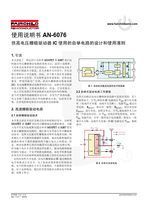
图 12. 情况 2 的 VB 和 VS 波形 VB=VBS+VS<0导致寄生二极管DBCOM导通VB被箝位在0V 一 种 实 用 的 电 路 可 能 处 在 以 上 两 种 极 限 之 间,结 果 是 VBS 电压稍微增大,和 VB 稍低于 VDD,如图 13 所示。
VB
VS
VB 䖥 COM VBS ࡴ
LS2
GND
- VS
D1
iLOAD iFree
V COUT
OUT
图 5. 降压转换器 图 6 描述了高端 N 沟道 MOSFET 关断期间的电压波形。
图 3. 半桥式应用电路
HIN
t
VS -COM
-VS
t
㓁⌕
图 4. 关断期间的 VS 波形
A⚍
VBS
B⚍ C⚍ VGS=B-C П䯈
VDC+VGSˈᆚࢦ VDC
㛝ކথ⫳఼
IN
䌃䗮⬉⌕㸹ٓᷙᵕ偅ࡼ఼
VB
UVLO
HO
RR
ాໄ⍜䰸఼
S
Q
VS
图 1. 高端驱动集成电路的电平转换器
2.2 自举式驱动电路工作原理
自举式电路在高电压栅极驱动电路中是很有用的,其工
作原理如下。当 VS 降低到 IC 电源电压 VDD 或下拉至地 时 (低端开关导通,高端开关关断),电源 VDD 通过自 举电阻, RBOOT,和自举二极管, DBOOT,对自举电容 CBOOT,进行充电,如图 2 所示。当 VS 被高端开关上拉 到一个较高电压时,由 VBS 对该自举电容充电,此时, VBS 电源浮动,自举二极管处于反向偏置,轨电压 (低 端开关关断,高端开关导通)和 IC 电源电压 VDD,被隔 离开。
- 1、下载文档前请自行甄别文档内容的完整性,平台不提供额外的编辑、内容补充、找答案等附加服务。
- 2、"仅部分预览"的文档,不可在线预览部分如存在完整性等问题,可反馈申请退款(可完整预览的文档不适用该条件!)。
- 3、如文档侵犯您的权益,请联系客服反馈,我们会尽快为您处理(人工客服工作时间:9:00-18:30)。
3
98C-1 Tape
Polyimide Film With Silicone Adhesive Datasheet
Product Description
3M TM Electrical Tape 98C-1 is a 1-mil polyimide backing with silicone adhesive. It is designed for high temperature application, used on coils, capacitors and wire harness.
l1-mil polyimide backing
l Silicone adhesive
l UL recognized, file number E256906
l Supplied on 3 inch cores
Like all 3M insulation tapes, 3M 98C-1 Tape is available in standard and custom widths and lengths. Standard length is 36 yards.
l Longer length up to several times normal length, dependent upon width. Check with Customer Service. Applications
3M TM 98C-1 tape is used for high temperature electrical application in which a tough, thin insulation material is required for wrapping coils, transformers, capacitors and wire harness. It’s also used in printed circuit board assembly as a wave solder masking tape.
Properties Typical Values
Type of Backing Polyimide
Type of Adhesive Silicone
Thickness (backing plus adhesive) 0.070mm Temperature rating 220o C
Breaking strength 125 lb./in (46N/10mm) Elongation 140%
Adhesion strength 121oz./in (2.3N/10mm) Dielectric Breakdown 16000 volts Electrolytic corrosion factor 2 1.0
UL Flame Retardant 3Yes
Footnote: 1. Test method ASTM D 1000
2. 3M test method
3. UL recognized flame retardant, Product Category OANZ2, File E256906.
3M is a trademark of 3M Company.
Important Notice
All statements, technical information, and recommendations related to 3M's products are based on information believed to be reliable, but the accuracy or completeness thereof is not guaranteed. Before using this product, you must evaluate it and determine if it is suitable for your intended application. You assume all risks and liability associated with such use. Any statements or recommendations related to the product , which are not contained in 3M’s current publications, or any contrary statements contained on your purchase order shall have no force or effect unless expressly agreed upon, in writing, by an authorized officer of 3M.
Warranty; Limited Remedy; Limited Liability.
This product will be free from defects in material and manufacture as of the date of purchase. 3M MAKES NO OTHER WARRANTIES INCLUDING, BUT NOT LIMITED TO, ANY IMPLIED WARRANTY OF MERCHANTABILITY OR FITNESS FOR A PARTICULAR PURPOSE. If this product is defective within the warranty period stated above, your exclusive remedy shall be, at 3M’s option, to replace or repair the 3M product or refund the purchase price of the 3M product. Except where prohibited by law, 3M will not be liable for any loss or damage arising from this 3M product, whether direct, Indirect, special, Incidental or consequential regardless of the legal theory asserted.
3
Electrical Markets Division © 3M August 2007。