AM29DL322GB120中文资料
BSM200GB120DLC中文资料
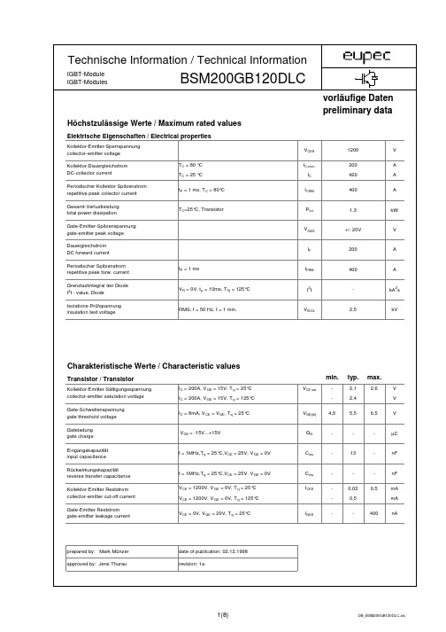
TC=25°C, Transistor
Ptot
1,3
kW
VGES
+/- 20V
V
IF
200
A
IFRM
400
A
VR = 0V, t p = 10ms, T Vj = 125°C
2 I t
-
kA2s
RMS, f = 50 Hz, t = 1 min.
VISOL
2,5
kV
Charakteristische Werte / Characteristic values
Transistor / Transistor
Kollektor-Emitter Sättigungsspannung collector-emitter saturation voltage Gate-Schwellenspannung gate threshold voltage Gateladung gate charge Eingangskapazität input capacitance Rückwirkungskapazität reverse transfer capacitance Kollektor-Emitter Reststrom collector-emitter cut-off current Gate-Emitter Reststrom gate-emitter leakage current IC = 200A, V GE = 15V, Tvj = 25°C IC = 200A, V GE = 15V, Tvj = 125°C IC = 8mA, V CE = VGE, Tvj = 25°C VGE(th) VCE sat
Elektrische Eigenschaften / Electrical properties
LM2902DR中文资料
元器件交易网元器件交易网IMPORTANT NOTICETexas Instruments Incorporated and its subsidiaries (TI) reserve the right to make corrections, modifications,enhancements, improvements, and other changes to its products and services at any time and to discontinueany product or service without notice. Customers should obtain the latest relevant information before placingorders and should verify that such information is current and complete. All products are sold subject to TI’s termsand conditions of sale supplied at the time of order acknowledgment.TI warrants performance of its hardware products to the specifications applicable at the time of sale inaccordance with TI’s standard warranty. T esting and other quality control techniques are used to the extent TIdeems necessary to support this warranty. Except where mandated by government requirements, testing of allparameters of each product is not necessarily performed.TI assumes no liability for applications assistance or customer product design. Customers are responsible fortheir products and applications using TI components. T o minimize the risks associated with customer productsand applications, customers should provide adequate design and operating safeguards.TI does not warrant or represent that any license, either express or implied, is granted under any TI patent right,copyright, mask work right, or other TI intellectual property right relating to any combination, machine, or processin which TI products or services are used. Information published by TI regarding third-party products or servicesdoes not constitute a license from TI to use such products or services or a warranty or endorsement thereof.Use of such information may require a license from a third party under the patents or other intellectual propertyof the third party, or a license from TI under the patents or other intellectual property of TI.Reproduction of information in TI data books or data sheets is permissible only if reproduction is withoutalteration and is accompanied by all associated warranties, conditions, limitations, and notices. Reproductionof this information with alteration is an unfair and deceptive business practice. TI is not responsible or liable forsuch altered documentation.Resale of TI products or services with statements different from or beyond the parameters stated by TI for thatproduct or service voids all express and any implied warranties for the associated TI product or service andis an unfair and deceptive business practice. TI is not responsible or liable for any such statements.Following are URLs where you can obtain information on other Texas Instruments products and applicationsolutions:Products ApplicationsAmplifiers Audio /audioData Converters Automotive /automotiveDSP Broadband /broadbandInterface Digital Control /digitalcontrolLogic Military /militaryPower Mgmt Optical Networking /opticalnetworkMicrocontrollers Security /securityTelephony /telephonyVideo & Imaging /videoWireless /wirelessMailing Address:Texas InstrumentsPost Office Box 655303 Dallas, Texas 75265Copyright 2005, Texas Instruments Incorporated。
AM29LV800BT-120FD资料

Am29L V800BData SheetRETIREDPRODUCTThis product has been retired and is not recommended for designs. For new and current designs, S29AL008D supersedes Am29LV800B and is the factory-recommended migration path. Please refer to the S29AL008D datasheet for specifications and ordering information. Availability of this docu-ment is retained for reference and historical purposes only.July 2003The following document specifies Spansion memory products that are now offered by both Advanced Micro Devices and Fujitsu. Although the document is marked with the name of the company that originally developed the specification, these products will be offered to customers of both AMD and Fujitsu.Continuity of SpecificationsThere is no change to this datasheet as a result of offering the device as a Spansion product. Any changes that have been made are the result of normal datasheet improvement and are noted in the document revision summary, where supported. Future routine revisions will occur when appro-priate, and changes will be noted in a revision summary.For More InformationPlease contact your local AMD or Fujitsu sales office for additional information about Spansion memory solutions.Publication Number21490Revision G Amendment5Issue Date May 25, 2005THIS PAGE LEFT INTENTIONALLY BLANK.Product Selector Guide . . . . . . . . . . . . . . . . . . . . .6 Block Diagram . . . . . . . . . . . . . . . . . . . . . . . . . . . . 6 Connection Diagrams . . . . . . . . . . . . . . . . . . . . . . .7 Special Handling Instructions for FBGA Package ..9 Pin Configuration. . . . . . . . . . . . . . . . . . . . . . . . . . 9 Logic Symbol . . . . . . . . . . . . . . . . . . . . . . . . . . . . 9 Ordering Information . . . . . . . . . . . . . . . . . . . . . .10 Standard Products (10)Device Bus Operations . . . . . . . . . . . . . . . . . . . . .11 Table 1. Am29LV800B Device Bus Operations (11)Word/Byte Configuration (11)Requirements for Reading Array Data (11)Writing Commands/Command Sequences (11)Program and Erase Operation Status (12)Standby Mode (12)Automatic Sleep Mode (12)RESET#: Hardware Reset Pin (12)Output Disable Mode (12)Table 2. Am29LV800BT Top Boot BlockSector Addresses (13)Table 3. Am29LV800BB Bottom Boot BlockSector Addresses (13)Autoselect Mode (14)Table 4. Am29LV800B Autoselect Codes(High Voltage Method) (14)Sector Protection/Unprotection (14)Temporary Sector Unprotect (14)Figure 1. Temporary Sector Unprotect Operation (15)Figure 2. In-System Sector Protect/Sector Unprotect Algorithms (16)Hardware Data Protection (17)Command Definitions . . . . . . . . . . . . . . . . . . . . . 17 Reading Array Data (17)Reset Command (17)Autoselect Command Sequence (17)Word/Byte Program Command Sequence (18)Figure 3. Program Operation (18)Chip Erase Command Sequence (19)Sector Erase Command Sequence (19)Erase Suspend/Erase Resume Commands (19)Figure 4. Erase Operation (20)Table 1. Am29LV800B Command Definitions (21)Write Operation Status . . . . . . . . . . . . . . . . . . . . 22 DQ7: Data# Polling (22)Figure 5. Data# Polling Algorithm (22)RY/BY#: Ready/Busy# (22)DQ6: Toggle Bit I (23)DQ2: Toggle Bit II (23)Reading Toggle Bits DQ6/DQ2 (23)DQ5: Exceeded Timing Limits (23)Figure 6. Toggle Bit Algorithm (24)DQ3: Sector Erase Timer (24)Table 2. Write Operation Status (25)Absolute Maximum Ratings . . . . . . . . . . . . . . . . 26 Operating Ranges. . . . . . . . . . . . . . . . . . . . . . . . . 26 DC Characteristics . . . . . . . . . . . . . . . . . . . . . . . . 27 CMOS Compatible (27)Figure 9. I CC1 Current vs. Time (Showing Active andAutomatic Sleep Currents) (28)Figure 10. Typical I CC1 vs. Frequency (28)Test Conditions . . . . . . . . . . . . . . . . . . . . . . . . . . 29 Figure 11. Test Setup (29)Table 3. Test Specifications (29)Key to Switching Waveforms. . . . . . . . . . . . . . . . 29 Figure 12. Input Waveforms andMeasurement Levels (29)AC Characteristics . . . . . . . . . . . . . . . . . . . . . . . . 30 Read Operations (30)Figure 13. Read Operations Timings (30)Hardware Reset (RESET#) (31)Figure 14. RESET# Timings (31)Word/Byte Configuration (BYTE#) (32)Figure 15. BYTE# Timings for Read Operations (32)Figure 16. BYTE# Timings for Write Operations (32)Erase/Program Operations (33)Figure 17. Program Operation Timings (34)Figure 18. Chip/Sector Erase Operation Timings (35)Figure 19. Data# Polling Timings (DuringEmbedded Algorithms) (36)Figure 20. Toggle Bit Timings (DuringEmbedded Algorithms) (36)Figure 21. DQ2 vs. DQ6 (37)Temporary Sector Unprotect (37)Figure 22. Temporary Sector UnprotectTiming Diagram (37)Figure 23. Sector Protect/UnprotectTiming Diagram (38)Alternate CE# Controlled Erase/Program Operations 39Figure 24. Alternate CE# Controlled WriteOperation Timings (40)Erase and Programming Performance . . . . . . . 41 Latchup Characteristics. . . . . . . . . . . . . . . . . . . . 41 TSOP and SO Pin Capacitance . . . . . . . . . . . . . . 41 Data Retention. . . . . . . . . . . . . . . . . . . . . . . . . . . . 41 Physical Dimensions* . . . . . . . . . . . . . . . . . . . . . 42 TS 048—48-Pin Standard TSOP (42)TSR048—48-Pin Reverse TSOP (43)FBB 048—48-Ball Fine-Pitch Ball Grid Array (FBGA) 6 x 9 mm (44)SO 044—44-Pin Small Outline Package (45)Revision Summary . . . . . . . . . . . . . . . . . . . . . . . . 46This Data Sheet states AMD’s current technical specifications regarding the Product described herein. This Data Sheet may be revised by subsequent versions or modifications due to changes in technical specifications.Publication# 21490Rev: G Amendment/+5 Issue Date: May 25, 2005Am29LV800B8 Megabit (1 M x 8-Bit/512 K x 16-Bit)CMOS 3.0 Volt-only Boot Sector Flash Memory DISTINCTIVE CHARACTERISTICS•Single power supply operation—2.7 to 3.6 volt read and write operations for battery-powered applications •Manufactured on 0.32 µm process technology—Compatible with 0.5 µm Am29LV800 device •High performance—Access times as fast as 70 ns•Ultra low power consumption (typical values at 5 MHz)—200 nA Automatic Sleep mode current—200 nA standby mode current—7 mA read current—15 mA program/e+5rase current•Flexible sector architecture—One 16 Kbyte, two 8 Kbyte, one 32 Kbyte, and fifteen 64 Kbyte sectors (byte mode)—One 8 Kword, two 4 Kword, one 16 Kword, and fifteen 32 Kword sectors (word mode)—Supports full chip erase—Sector Protection features:A hardware method of locking a sector to preventany program or erase operations within that sectorSectors can be locked in-system or viaprogramming equipmentT emporary Sector Unprotect feature allows codechanges in previously locked sectors •Unlock Bypass Program Command —Reduces overall programming time when issuing multiple program command sequences •Top or bottom boot block configurations available •Embedded Algorithms—Embedded Erase algorithm automatically preprograms and erases the entire chip or anycombination of designated sectors—Embedded Program algorithm automatically writes and verifies data at specified addresses •Minimum 1 million write cycle guarantee per sector•20-year data retention at 125°C—Reliable operation for the life of the system •Package option—48-ball FBGA—48-pin TSOP—44-pin SO—Known Good Die (KGD)(see publication number 21536)•Compatibility with JEDEC standards —Pinout and software compatible with single-power supply Flash—Superior inadvertent write protection•Data# Polling and toggle bits—Provides a software method of detecting program or erase operation completion •Ready/Busy# pin (RY/BY#)—Provides a hardware method of detecting program or erase cycle completion•Erase Suspend/Erase Resume—Suspends an erase operation to read data from, or program data to, a sector that is not beingerased, then resumes the erase operation •Hardware reset pin (RESET#)—Hardware method to reset the device to reading array dataFor new designs, S29AL008D supersedes Am29LV800B and is the factory-recommended migration path for this device. Please refer to the S29AL008D Family Datasheet for specifications and ordering information.GENERAL DESCRIPTIONThe Am29LV800B is an 8 Mbit, 3.0 volt-only Flash memory organized as 1,048,576 bytes or 524,288 words. The device is offered in 48-ball FBGA, 44-pin SO, and 48-pin TSOP packages. The device is also available in Known Good Die (KGD) form. For more information, refer to publication number 21536. The word-wide data (x16) appears on DQ15–DQ0; the byte-wide (x8) data appears on DQ7–DQ0. This device requires only a single, 3.0 volt V CC supply to perform read, program, and erase operations. A stan-dard EPROM programmer can also be used to program and erase the device.This device is manufactured using AMD’s 0.32 µm process technology, and offers all the features and benefits of the Am29LV800, which was manufactured using 0.5 µm process technology. In addition, the Am29LV800B features unlock bypass programming and in-system sector protection/unprotection.The standard device offers access times of 70, 90, and 120 ns, allowing high speed microprocessors to operate without wait states. To eliminate bus conten-tion the device has separate chip enable (CE#), write enable (WE#) and output enable (OE#) controls.The device requires only a single 3.0 volt power supply for both read and write functions. Internally generated and regulated voltages are provided for the program and erase operations.The device is entirely command set compatible with the JEDEC single-power-supply Flash standard. Commands are written to the command register using standard microprocessor write timings. Reg-ister contents serve as input to an internal state-machine that controls the erase and programming circuitry. Write cycles also internally latch addresses and data needed for the programming and erase operations. Reading data out of the device is similar to reading from other Flash or EPROM devices. Device programming occurs by executing the program command sequence. This initiates the Embedded Program algorithm—an internal algo-rithm that automatically times the program pulse widths and verifies proper cell margin. The Unlock Bypass mode facilitates faster programming times by requiring only two write cycles to program data instead of four.Device erasure occurs by executing the erase command sequence. This initiates the Embedded Erase algorithm—an internal algorithm that auto-matically preprograms the array (if it is not already programmed) before executing the erase operation. During erase, the device automatically times the erase pulse widths and verifies proper cell margin. The host system can detect whether a program or erase operation is complete by observing the RY/BY# pin, or by reading the DQ7 (Data# Polling) and DQ6 (toggle) status bits. After a program or erase cycle has been completed, the device is ready to read array data or accept another command.The sector erase architecture allows memory sectors to be erased and reprogrammed without affecting the data contents of other sectors. The device is fully erased when shipped from the factory. Hardware data protection measures include a low V CC detector that automatically inhibits write opera-tions during power transitions. The hardware sector protection feature disables both program and erase operations in any combination of the sectors of memory. This can be achieved in-system or via pro-gramming equipment.The Erase Suspend feature enables the user to put erase on hold for any period of time to read data from, or program data to, any sector that is not selected for erasure. True background erase can thus be achieved.The hardware RESET# pin terminates any opera-tion in progress and resets the internal state machine to reading array data. The RESET# pin may be tied to the system reset circuitry. A system reset would thus also reset the device, enabling the system micropro-cessor to read the boot-up firmware from the Flash memory.The device offers two power-saving features. When addresses have been stable for a specified amount of time, the device enters the automatic sleep mode. The system can also place the device into the standby mode. Power consumption is greatly reduced in both these modes.AMD’s Flash technology combines years of Flash memory manufacturing experience to produce the highest levels of quality, reliability and cost effective-ness. The device electrically erases all bits within a sector simultaneously via Fowler-Nordheim tun-neling. The data is programmed using hot electron injection.T ABLE OF CONTENTSProduct Selector Guide . . . . . . . . . . . . . . . . . . . . .6 Block Diagram . . . . . . . . . . . . . . . . . . . . . . . . . . . . 6 Connection Diagrams . . . . . . . . . . . . . . . . . . . . . . .7 Special Handling Instructions for FBGA Package ..9 Pin Configuration. . . . . . . . . . . . . . . . . . . . . . . . . . 9 Logic Symbol . . . . . . . . . . . . . . . . . . . . . . . . . . . . 9 Ordering Information . . . . . . . . . . . . . . . . . . . . . .10 Standard Products (10)Device Bus Operations . . . . . . . . . . . . . . . . . . . . .11 Table 1. Am29LV800B Device Bus Operations (11)Word/Byte Configuration (11)Requirements for Reading Array Data (11)Writing Commands/Command Sequences (11)Program and Erase Operation Status (12)Standby Mode (12)Automatic Sleep Mode (12)RESET#: Hardware Reset Pin (12)Output Disable Mode (12)Table 2. Am29LV800BT Top Boot BlockSector Addresses (13)Table 3. Am29LV800BB Bottom Boot BlockSector Addresses (13)Autoselect Mode (14)Table 4. Am29LV800B Autoselect Codes(High Voltage Method) (14)Sector Protection/Unprotection (14)Temporary Sector Unprotect (14)Figure 1. Temporary Sector Unprotect Operation (15)Figure 2. In-System Sector Protect/Sector Unprotect Algorithms (16)Hardware Data Protection (17)Command Definitions . . . . . . . . . . . . . . . . . . . . . 17 Reading Array Data (17)Reset Command (17)Autoselect Command Sequence (17)Word/Byte Program Command Sequence (18)Figure 3. Program Operation (18)Chip Erase Command Sequence (19)Sector Erase Command Sequence (19)Erase Suspend/Erase Resume Commands (19)Figure 4. Erase Operation (20)Table 1. Am29LV800B Command Definitions (21)Write Operation Status . . . . . . . . . . . . . . . . . . . . 22 DQ7: Data# Polling (22)Figure 5. Data# Polling Algorithm (22)RY/BY#: Ready/Busy# (22)DQ6: Toggle Bit I (23)DQ2: Toggle Bit II (23)Reading Toggle Bits DQ6/DQ2 (23)DQ5: Exceeded Timing Limits (23)Figure 6. Toggle Bit Algorithm (24)DQ3: Sector Erase Timer (24)Table 2. Write Operation Status (25)Absolute Maximum Ratings . . . . . . . . . . . . . . . . 26 Operating Ranges. . . . . . . . . . . . . . . . . . . . . . . . . 26 DC Characteristics . . . . . . . . . . . . . . . . . . . . . . . . 27 CMOS Compatible (27)Figure 9. I CC1 Current vs. Time (Showing Active andAutomatic Sleep Currents) (28)Figure 10. Typical I CC1 vs. Frequency (28)Test Conditions . . . . . . . . . . . . . . . . . . . . . . . . . . 29 Figure 11. Test Setup (29)Table 3. Test Specifications (29)Key to Switching Waveforms. . . . . . . . . . . . . . . . 29 Figure 12. Input Waveforms andMeasurement Levels (29)AC Characteristics . . . . . . . . . . . . . . . . . . . . . . . . 30 Read Operations (30)Figure 13. Read Operations Timings (30)Hardware Reset (RESET#) (31)Figure 14. RESET# Timings (31)Word/Byte Configuration (BYTE#) (32)Figure 15. BYTE# Timings for Read Operations (32)Figure 16. BYTE# Timings for Write Operations (32)Erase/Program Operations (33)Figure 17. Program Operation Timings (34)Figure 18. Chip/Sector Erase Operation Timings (35)Figure 19. Data# Polling Timings (DuringEmbedded Algorithms) (36)Figure 20. Toggle Bit Timings (DuringEmbedded Algorithms) (36)Figure 21. DQ2 vs. DQ6 (37)Temporary Sector Unprotect (37)Figure 22. Temporary Sector UnprotectTiming Diagram (37)Figure 23. Sector Protect/UnprotectTiming Diagram (38)Alternate CE# Controlled Erase/Program Operations 39Figure 24. Alternate CE# Controlled WriteOperation Timings (40)Erase and Programming Performance . . . . . . . 41 Latchup Characteristics. . . . . . . . . . . . . . . . . . . . 41 TSOP and SO Pin Capacitance . . . . . . . . . . . . . . 41 Data Retention. . . . . . . . . . . . . . . . . . . . . . . . . . . . 41 Physical Dimensions* . . . . . . . . . . . . . . . . . . . . . 42 TS 048—48-Pin Standard TSOP (42)TSR048—48-Pin Reverse TSOP (43)FBB 048—48-Ball Fine-Pitch Ball Grid Array (FBGA) 6 x 9 mm (44)SO 044—44-Pin Small Outline Package (45)Revision Summary . . . . . . . . . . . . . . . . . . . . . . . . 46PRODUCT SELECTOR GUIDENote: See “AC Characteristics” for full specifications.BLOCK DIAGRAMFamily Part Number Am29LV800BSpeed OptionsFull Voltage Range: V CC = 2.7–3.6 V-70-90-120Max access time, ns (t ACC )7090120Max CE# access time, ns (t CE )7090120Max OE# access time, ns (t OE )303550Input/OutputBuffers X-DecoderY-Decoder Chip Enable Output EnableLogicErase Voltage GeneratorPGM Voltage GeneratorTimerV CC DetectorState Control Command RegisterV CC V SS WE#BYTE#CE#OE#STBSTBDQ0–DQ15 (A-1)Sector Switches RY/BY#RESET#Data LatchY-GatingCell MatrixA d d r e s s L a t c hA0–A18CONNECTION DIAGRAMSThis device is also available in Known Good Die (KGD) form. Refer to publication number 21536 for more information.CONNECTION DIAGRAMSThis device is also available in Known Good Die (KGD) form. Refer to publication number 21536 for more information.Special Handling Instructions for FBGA PackageSpecial handling is required for Flash Memory prod-ucts in FBGA packages.Flash memory devices in FBGA packages may be damaged if exposed to ultrasonic cleaning methods. The package and/or data integrity may be compro-mised if the package body is exposed to temperatures above 150°C for prolonged periods of time.PIN CONFIGURATIONA0–A18=19 addressesDQ0–DQ14=15 data inputs/outputsDQ15/A-1=DQ15 (data input/output, wordmode),A-1 (LSB address input, bytemode)BYTE#=Selects 8-bit or 16-bit modeCE#=Chip enableOE#= Output enableWE#=Write enableRESET#=Hardware reset pin, active low RY/BY#= Ready/Busy# outputV CC= 3.0 volt-only single power supply(see Product Selector Guide forspeedoptions and voltage supplytolerances)V SS=Device ground NC=Pin not connected internally LOGIC SYMBOL1916 or 8DQ0–DQ15(A-1)A0–A18CE#OE#WE#RESET#BYTE#RY/BY#ORDERING INFORMATION Standard ProductsAMD standard products are available in several packages and operating ranges. The order number (Valid Com-bination) is formed by a combination of the elements below.Valid CombinationsValid Combinations list configurations planned to be supported in volume for this device. Consult the local AMD sales office to confirm availability of specific valid combinations and to check on newly released combinations.Am29LV800BT-70ECTEMPERATURE RANGE C =Commercial (0°C to +70°C)D =Commercial (0°C to +70°C) with Pb-free package I = Industrial (–40°C to +85°C)F =Industrial (–40°C to +85°C) with Pb-free package E =Extended (–55°C to +125°C)K =Extended (–55°C to +125°C) with Pb-free packagePACKAGE TYPE E =48-Pin Thin Small Outline Package (TSOP) Standard Pinout (TS 048)F =48-Pin Thin Small Outline Package (TSOP) Reverse Pinout (TSR048)S =44-Pin Small Outline Package (SO 044)WB =48-Ball Fine Pitch Ball Grid Array (FBGA)0.80 mm pitch, 6 x 9 mm package (FBB048)This device is also available in Known Good Die (KGD) form. See publication number 21536 for more information.SPEED OPTIONSee Product Selector Guide and Valid CombinationsBOOT CODE SECTOR ARCHITECTURE T = Top sector B = Bottom sectorDEVICE NUMBER/DESCRIPTIONAm29LV800B8 Megabit (1 M x 8-Bit/512 K x 16-Bit) CMOS Flash Memory 3.0 Volt-only Read, Program, and EraseValid Combinations for TSOP and SO PackagesAM29LV800BT-70, AM29LV800BB-70EC, EI, FC, FI, SC, SI,ED, EF , SD, SF AM29LV800BT-90, AM29LV800BB-90EC, EI, EE, ED, EFFC, FI, FE,SC, SI, SE, SD, SF , EK, SKAM29LV800BT-120, AM29LV800BB-120Valid Combinations for FBGA Packages Order NumberPackage MarkingAM29LV800BT-70, AM29LV800BB-70WBC,WBD,WBI,WBF L800BT70V , L800BB70V C, D,I, FAM29LV800BT-90, AM29LV800BB-90WBC, WBI,WBD,WBF ,WBK,WBEL800BT90V , L800BB90V C, I,D, F K, EAM29LV800BT-120, AM29LV800BB-120L800BT12V , L800BB12VDEVICE BUS OPERATIONSThis section describes the requirements and use of the device bus operations, which are initiated through the internal command register. The command reg-ister itself does not occupy any addressable memory location. The register is composed of latches that store the commands, along with the address and data information needed to execute the command. The contents of the register serve as inputs to the internal state machine. The state machine outputs dictate the function of the device. Table 1 lists the device bus operations, the inputs and control levels they require, and the resulting output. The following subsections describe each of these operations in further detail.Table 1. Am29LV800B Device Bus OperationsLegend:L = Logic Low = V IL, H = Logic High = V IH, V ID = 12.0 ± 0.5 V, X = Don’t Care, A IN = Address In, D IN = Data In, D OUT = Data Out Notes:1.Addresses are A18:A0 in word mode (BYTE# = V IH), A18:A-1 in byte mode (BYTE# = V IL).2.The sector protect and sector unprotect functions may also be implemented via programming equipment. See the “SectorProtection/Unprotection” section.Word/Byte ConfigurationThe BYTE# pin controls whether the device data I/O pins DQ15–DQ0 operate in the byte or word configu-ration. If the BYTE# pin is set at logic ‘1’, the device is in word configuration, DQ15–DQ0 are active and controlled by CE# and OE#.If the BYTE# pin is set at logic ‘0’, the device is in byte configuration, and only data I/O pins DQ0–DQ7 are active and controlled by CE# and OE#. The data I/O pins DQ8–DQ14 are tri-stated, and the DQ15 pin is used as an input for the LSB (A-1) address function. Requirements for Reading Array DataTo read array data from the outputs, the system must drive the CE# and OE# pins to V IL. CE# is the power control and selects the device. OE# is the output control and gates array data to the output pins. WE# should remain at V IH. The BYTE# pin determines whether the device outputs array data in words or bytes.The internal state machine is set for reading array data upon device power-up, or after a hardware reset. This ensures that no spurious alteration of the memory content occurs during the power transition. No command is necessary in this mode to obtain array data. Standard microprocessor read cycles that assert valid addresses on the device address inputs produce valid data on the device data outputs. The device remains enabled for read access until the command register contents are altered.See “Reading Array Data” for more information. Refer to the AC Read Operations table for timing specifica-tions and to Figure 13 for the timing diagram. I CC1 in the DC Characteristics table represents the active current specification for reading array data. Writing Commands/Command Sequences To write a command or command sequence (which includes programming data to the device and erasing sectors of memory), the system must drive WE# and CE# to V IL, and OE# to V IH.For program operations, the BYTE# pin determines whether the device accepts program data in bytes or words. Refer to “Word/Byte Configuration” for more information.Operation CE#OE#WE#RESET#Addresses(Note 1)DQ0–DQ7DQ8–DQ15BYTE#= V IHBYTE#= V ILRead L L H H A IN D OUT D OUT DQ8–DQ14 = High-Z,DQ15 = A-1 Write L H L H A IN D IN D INStandby V CC±0.3 VX XV CC±0.3 VX High-Z High-Z High-ZOutput Disable L H H H X High-Z High-Z High-Z Reset X X X L X High-Z High-Z High-ZSector Protect (Note 2)L H L V ID Sector Address,A6 = L, A1 = H,A0 = LD IN X XSector Unprotect (Note 2)L H L V ID Sector Address,A6 = H, A1 = H,A0 = LD IN X XTemporary Sector Unprotect X X X V ID A IN D IN D IN High-ZThe device features an Unlock Bypass mode to facil-itate faster programming. Once the device enters the Unlock Bypass mode, only two write cycles are required to program a word or byte, instead of four. The “Word/Byte Program Command Sequence”section has details on programming data to the device using both standard and Unlock Bypass command sequences.An erase operation can erase one sector, multiple sec-tors, or the entire device. Tables 2 and 3 indicate the address space that each sector occupies. A “sector address” consists of the address bits required to uniquely select a sector. The “Command Definitions”section has details on erasing a sector or the entire chip, or suspending/resuming the erase operation. After the system writes the autoselect command sequence, the device enters the autoselect mode. The system can then read autoselect codes from the internal register (which is separate from the memory array) on DQ7–DQ0. Standard read cycle timings apply in this mode. Refer to the “Autoselect Mode”and “Autoselect Command Sequence” sections for more information.I CC2 in the DC Characteristics table represents the active current specification for the write mode. The “AC Characteristics” section contains timing specifica-tion tables and timing diagrams for write operations. Program and Erase Operation Status During an erase or program operation, the system may check the status of the operation by reading the status bits on DQ7–DQ0. Standard read cycle timings and I CC read specifications apply. Refer to “Write Operation Status” for more information, and to “AC Characteristics” for timing diagrams.Standby ModeWhen the system is not reading or writing to the device, it can place the device in the standby mode. In this mode, current consumption is greatly reduced, and the outputs are placed in the high impedance state, independent of the OE# input.The device enters the CMOS standby mode when the CE# and RESET# pins are both held at V CC ± 0.3 V. (Note that this is a more restricted voltage range than V IH.) If CE# and RESET# are held at V IH, but not within V CC ± 0.3 V, the device will be in the standby mode, but the standby current will be greater. The device requires standard access time (t CE) for read access when the device is in either of these standby modes, before it is ready to read data.If the device is deselected during erasure or program-ming, the device draws active current until the operation is completed.In the DC Characteristics table, I CC3 and I CC4 repre-sents the standby current specification. Automatic Sleep ModeThe automatic sleep mode minimizes Flash device energy consumption. The device automatically enables this mode when addresses remain stable for t ACC + 30 ns. The automatic sleep mode is indepen-dent of the CE#, WE#, and OE# control signals. Stan-dard address access timings provide new data when addresses are changed. While in sleep mode, output data is latched and always available to the system.I CC4 in the DC Characteristics table represents the automatic sleep mode current specification. RESET#: Hardware Reset PinThe RESET# pin provides a hardware method of resetting the device to reading array data. When the RESET# pin is driven low for at least a period of t RP, the device immediately terminates any operation in progress, tristates all output pins, and ignores all read/write commands for the duration of the RESET# pulse. The device also resets the internal state machine to reading array data. The operation that was interrupted should be reinitiated once the device is ready to accept another command sequence, to ensure data integrity.Current is reduced for the duration of the RESET# pulse. When RESET# is held at V SS±0.3 V, the device draws CMOS standby current (I CC4). If RESET# is held at V IL but not within V SS±0.3 V, the standby current will be greater.The RESET# pin may be tied to the system reset cir-cuitry. A system reset would thus also reset the Flash memory, enabling the system to read the boot-up firmware from the Flash memory.If RESET# is asserted during a program or erase operation, the RY/BY# pin remains a “0” (busy) until the internal reset operation is complete, which requires a time of t READY (during Embedded Algo-rithms). The system can thus monitor RY/BY# to determine whether the reset operation is complete. If RESET# is asserted when a program or erase opera-tion is not executing (RY/BY# pin is “1”), the reset operation is completed within a time of t READY (not during Embedded Algorithms). The system can read data t RH after the RESET# pin returns to V IH.Refer to the AC Characteristics tables for RESET# parameters and to Figure 14 for the timing diagram. Output Disable Mode。
ZXT2M322TA;中文规格书,Datasheet资料
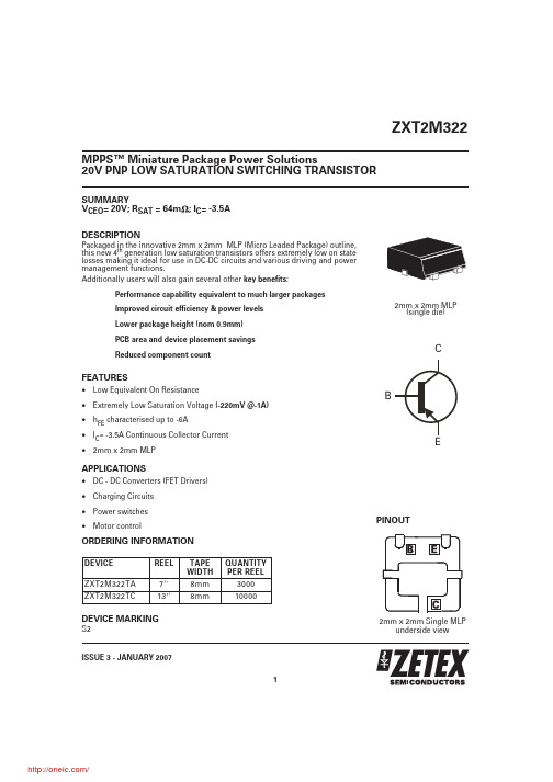
SUMMARYV CEO = 20V;R SAT = 64m ;I C = -3.5A DESCRIPTIONPackaged in the innovative 2mm x 2mm MLP (Micro Leaded Package)outline,this new 4th generation low saturation transistors offers extremely low on state losses making it ideal for use in DC-DC circuits and various driving and power management functions.Additionally users will also gain several other key benefits :Performance capability equivalent to much larger packages Improved circuit efficiency & power levels Lower package height (nom 0.9mm)PCB area and device placement savings Reduced component countFEATURES•Low Equivalent On Resistance•Extremely Low Saturation Voltage (-220mV @-1A)•h FE characterised up to -6A•I C = -3.5A Continuous Collector Current •2mm x 2mm MLPAPPLICATIONS•DC - DC Converters (FET Drivers)•Charging Circuits •Power switches •Motor controlORDERING INFORMATIONDEVICE MARKINGS2ZXT2M322ISSUE 3 - JANUARY 20071MPPS™Miniature Package Power Solutions20V PNP LOW SATURATION SWITCHING TRANSISTOR2mm x 2mm Single MLPunderside viewPINOUTDEVICE REEL TAPE WIDTH QUANTITY PER REELZXT2M322TA 78mm 3000ZXT2M322TC138mm100002mm x 2mm MLP(single die)ZXT2M322ISSUE 3 - JANUARY 20072PARAMETERSYMBOL VALUE UNIT Junction to Ambient (a)R θJA 83°C/W Junction to Ambient (b)R θJA 51°C/W Junction to Ambient (d)R θJA 125°C/W Junction to Ambient (e)R θJA42°C/WTHERMAL RESISTANCENOTES(a) For a single device surface mounted on 10sq cm1oz copper on FR4 PCB in still air conditions with all exposed pads attached .(b) For a single device surface mounted on 10sq cm1oz copper on FR4 PCB in still air conditions measured at t р5 secs with all exposed pads attached.(c) Repetitive rating - pulse width limited by max junction temperature. refer to Transient Thermal Impedance graph.(d) For a single device surface mounted on 10sq cm1oz copper on FR4 PCB in still air conditions with minimal lead connections only .(e) For a single device surface mounted on 65sq cm2oz copper on FR4 PCB in still air conditions with all exposed pads attached .(f) The minimum copper dimensions required for mounting are no smaller than the exposed metal pads on the base of the device, as shown in the package dimensions data. The thermal resistance for a device mounted on 1.5mm thick FR4 board using minimum copper of 1oz weight is Rth=300°C/W giving a power rating of Ptot=420mW.PARAMETERSYMBOL LIMIT UNIT Collector-Base Voltage V CBO -25V Collector-Emitter Voltage V CEO -20V Emitter-Base Voltage V EBO -7.5V Peak Pulse Current (c)I CM -6A Continuous Collector Current (a)I C -3.5A Base CurrentI B -1000mA Power Dissipation at TA=25°C (a)Linear Derating FactorP D 1.512W mW/°C Power Dissipation at TA=25°C (b)Linear Derating FactorP D 2.4519.6W mW/°C Power Dissipation at TA=25°C (d)Linear Derating FactorP D 18W mW/°C Power Dissipation at TA=25°C (e)Linear Derating FactorP D 324W mW/°C Operating and Storage Temperature RangeT j :T stg-55 to +150°CABSOLUTE MAXIMUM RATINGS.ZXT2M322ISSUE 3 - JANUARY 20073CHARACTERISTICSCHARACTERISTICSZXT2M322ISSUE 3 - JANUARY 20074PARAMETERSYMBOL MIN.TYP.MAX.UNIT CONDITIONS.Collector-Base Breakdown VoltageV (BR)CBO -25-35V I C =-100A Collector-Emitter Breakdown VoltageV (BR)CEO -20-25V I C =-10mA*Emitter-Base Breakdown Voltage V (BR)EBO -7.5-8.5V I E =-100A Collector Cut-Off Current I CBO -25nA V CB =-20V Emitter Cut-Off CurrentI EBO -25nA V EB =-6V Collector Emitter Cut-Off Current I CES -25nA V CES =-16VCollector-Emitter Saturation VoltageV CE(sat)-19-170-190-240-225-30-220-250-350-300mV mV mV mV mVI C =-0.1A,I B =-10mA*I C =-1A,I B =-20mA*I C =-1.5A,I B =-50mA*I C =-2.5A,I B =-150mA*I C =-3.5A,I B =-350mA*Base-Emitter Saturation Voltage V BE(sat)-1.01-1.075V I C =-3.5A,I B =-350mA*Base-Emitter Turn-On Voltage V BE(on)-0.87-0.95VI C =-3.5A,V CE =-2V*Static Forward Current Transfer Ratioh FE3003001501547545023030I C =-10mA,V CE =-2V*I C =-0.1A,V CE =-2V*I C =-2A,V CE =-2V*I C =-6A,V CE =-2V*Transition Frequency f T 150180MHz I C =-50mA,V CE =-10V f=100MHzOutput Capacitance C obo 2130pF V CB =-10V,f=1MHz Turn-On Time t (on)40ns V CC =-10V,I C =-1A I B1=I B2=10mATurn-Off Timet (off)670nsELECTRICAL CHARACTERISTICS (at T amb = 25°C unless otherwise stated).*Measured under pulsed conditions. Pulse width=300µs. Duty cycle ≤2%ISSUE 3 - JANUARY 20075ZXT2M322ISSUE 3 - JANUARY 20076EuropeZetex GmbH Balan-straße 59D-81541 München GermanyTelefon: (49) 89 45 49 49 0Fax: (49) 89 45 49 49 49europe.sales@AmericasZetex Inc700 Veterans Memorial Hwy Hauppauge, NY11788USATelephone: (631) 360 2222Fax: (631) 360 8222usa.sales@Asia PacificZetex (Asia) Ltd3701-04Metroplaza, Tower 1Hing Fong Road Kwai Fong Hong KongTelephone: (852) 26100 611Fax: (852) 24250 494asia.sales@Corporate Headquarters Zetex Semiconductors plc Zetex Technology Park ChaddertonOldham, OL9 9LL United KingdomTel: (44) 161 622 4444Fax: (44) 161 622 4446hq@These offices are supported by agents and distributors in major countries world-wide.This publication is issued to provide outline information only which (unless agreed by the Company in writing)may not be used,applied or reproduced for any purpose or form part of any order or contract or be regarded as a representation relating to the products or services concerned.The Company reserves the right to alter without notice the specification,design,price or conditions of supply of any product or service.For the latest product information,log on to©ZetexSemiconductors plc 2007CONTROLLING DIMENSIONS IN MILLIMETRES APPROX. CONVERTED DIMENSIONS IN INCHESMLP322 PACKAGE OUTLINE (2mm x 2mm Micro Leaded Package)DIM MILLIMETRESINCHES DIM MILLIMETRES INCHES MIN.MAX.MIN.MAX.MIN.MAX.MIN.MAX.A 0.80 1.000.03150.0393e 0.65REF 0.0255REF A10.000.050.000.002E 2.00BSC 0.0787BSC A20.650.750.02550.0295E20.790.990.0310.039A30.150.250.00590.0098E40.480.680.01880.0267b 0.180.280.00700.0110L 0.200.450.00780.0177b10.170.300.00660.0118L20.125MAX.0.005REF D 2.00BSC 0.0787BSCr 0.075BSC 0.0029BSC D2 1.22 1.420.04800.0559⍜0Њ12Њ0Њ12ЊD40.560.760.02200.0299PACKAGE DIMENSIONS分销商库存信息: DIODESZXT2M322TA。
AM29F032B-90EE中文资料

-XO\7KH IROORZLQJ GRFXPHQW VSHFLILHV 6SDQVLRQ PHPRU\ SURGXFWV WKDW DUH QRZ RIIHUHG E\ ERWK $GYDQFHG 0LFUR 'HYLFHV DQG )XMLWVX $OWKRXJK WKH GRFXPHQW LV PDUNHG ZLWK WKH QDPH RI WKH FRPSDQ\ WKDW RULJ LQDOO\ GHYHORSHG WKH VSHFLILFDWLRQ WKHVH SURGXFWV ZLOO EH RIIHUHG WR FXVWRPHUV RI ERWK $0' DQG )XMLWVXContinuity of Specifications7KHUH LV QR FKDQJH WR WKLV GDWDVKHHW DV D UHVXOW RI RIIHULQJ WKH GHYLFH DV D 6SDQVLRQ SURGXFW $Q\FKDQJHV WKDW KDYH EHHQ PDGH DUH WKH UHVXOW RI QRUPDO GDWDVKHHW LPSURYHPHQW DQG DUH QRWHG LQ WKH GRFXPHQW UHYLVLRQ VXPPDU\ ZKHUH VXSSRUWHG )XWXUH URXWLQH UHYLVLRQV ZLOO RFFXU ZKHQ DSSURSULDWH DQG FKDQJHV ZLOO EH QRWHG LQ D UHYLVLRQ VXPPDU\Continuity of Ordering Part Numbers$0' DQG )XMLWVX FRQWLQXH WR VXSSRUW H[LVWLQJ SDUW QXPEHUV EHJLQQLQJ ZLWK ³$P´ DQG ³0%0´ 7R RUGHU WKHVH SURGXFWV SOHDVH XVH RQO\ WKH 2UGHULQJ 3DUW 1XPEHUV OLVWHG LQ WKLV GRFXPHQWFor More Information3OHDVH FRQWDFW \RXU ORFDO $0' RU )XMLWVX VDOHV RIILFH IRU DGGLWLRQDO LQIRUPDWLRQ DERXW 6SDQVLRQ PHPRU\ VROXWLRQVAm29F032BData SheetPublication Number 21610 Revision D Amendment +1 Issue Date December 5, 2000元器件交易网This Data Sheet states AMD’s current technical specifications regarding the Product described herein. This Data Sheet may be revised by subsequent versions or modifications due to changes in technical specifications.Publication# 21610Rev: D Amendment/+1 Issue Date: December 5, 2000Am29F032B32 Megabit (4 M x 8-Bit)CMOS 5.0 Volt-only, Uniform Sector Flash Memory DISTINCTIVE CHARACTERISTICSs 5.0 V ± 10%, single power supply operation —Minimizes system level power requirementss Manufactured on 0.32 µm process technologys High performance—Access times as fast as 70 nss Low power consumption—30 mA typical active read current—30 mA typical program/erase current—<1 µA typical standby current (standard access time to active mode)s Flexible sector architecture—64 uniform sectors of 64 Kbytes each—Any combination of sectors can be erased.—Supports full chip erase—Group sector protection:—A hardware method of locking sector groups to prevent any program or erase operations withinthat sector group—Temporary Sector Group Unprotect allows code changes in previously locked sectorss Embedded Algorithms—Embedded Erase algorithm automatically preprograms and erases the entire chip or anycombination of designated sectors—Embedded Program algorithm automatically writes and verifies bytes at specified addresses s Minimum 1,000,000 write/erase cyclesguaranteeds20-year data retention at 125°C—Reliable operation for the life of the systems Package options—40-pin TSOP—44-pin SOs Compatible with JEDEC standards—Pinout and software compatible withsingle-power-supply Flash standard—Superior inadvertent write protections Data# Polling and toggle bits—Provides a software method of detecting program or erase cycle completions Ready/Busy output (RY/BY#)—Provides a hardware method for detecting program or erase cycle completions Erase Suspend/Resume—Suspends a sector erase operation to read data from, or program data to, a non-erasing sector,then resumes the erase operations Hardware reset pin (RESET#)—Resets internal state machine to the read modeGENERAL DESCRIPTIONThe Am29F032B is a 32 Mbit, 5.0 volt-only Flash memory organized as 4,194,304 bytes of 8 bits each. The 4 Mbytes of data are divided into 64 sectors of 64 Kbytes each for flexible erase capability. The 8 bits of data appear on DQ0–DQ7. The Am29F032B is offered in 40-pin TSOP and 44-pin SO packages. The Am29F032B is manufactured using AMD’s 0.32 µm process technology. This device is designed to be pro-grammed in-system with the standard system 5.0 volt V CC supply. A 12.0 volt V PP is not required for program or erase operations. The device can also be pro-grammed in standard EPROM programmers.The standard device offers access times of 70, 90, 120, and 150 ns, allowing high-speed microprocessors to operate without wait states. To eliminate bus con-tention, the device has separate chip enable (CE#), write enable (WE#), and output enable (OE#) controls. The device is entirely command set compatible with the JEDEC single-power-supply Flash standard. Com-mands are written to the command register using stan-dard microprocessor write timings. Register contents serve as input to an internal state machine that con-trols the erase and programming circuitry. Write cycles also internally latch addresses and data needed for the programming and erase operations. Reading data out of the device is similar to reading from 12.0 volt Flash or EPROM devices.The device is programmed by executing the program command sequence. This invokes the Embedded Pro-gram algorithm—an internal algorithm that automati-cally times the program pulse widths and verifies proper cell margin. The device is erased by executing the erase command sequence. This invokes the Em-bedded Erase algorithm—an internal algorithm that automatically preprograms the array (if it is not already programmed) before executing the erase operation. During erase, the device automatically times the erase pulse widths and verifies proper cell margin.The sector erase architecture allows memory sectors to be erased and reprogrammed without affecting the data contents of other sectors. A sector is typically erased and verified within one second. The device is erased when shipped from the factory.The hardware sector group protection feature disables both program and erase operations in any combination of the eight sector groups of memory. A sector group consists of four adjacent sectors.The Erase Suspend feature enables the system to put erase on hold for any period of time to read data from, or program data to, a sector that is not being erased. True background erase can thus be achieved.The device requires only a single 5.0 volt power supply for both read and write functions. Internally generated and regulated voltages are provided for the program and erase operations. A low V CC detector automati-cally inhibits write operations during power transitions. The host system can detect whether a program or erase cycle is complete by using the RY/BY# pin, the DQ7 (Data# Polling) or DQ6 (toggle) status bits. After a program or erase cycle has been completed, the de-vice automatically returns to the read mode.A hardware RESET# pin terminates any operation in progress. The internal state machine is reset to the read mode. The RESET# pin may be tied to the sys-tem reset circuitry. Therefore, if a system reset occurs during either an Embedded Program or Embedded Erase algorithm, the device is automatically reset to the read mode. This enables the system’s microprocessor to read the boot-up firmware from the Flash memory. AMD’s Flash technology combines years of Flash memory manufacturing experience to produce the highest levels of quality, reliability, and cost effectiveness. The device electrically erases all bits within a sector simultaneously via Fowler-Nordheim tunneling. The bytes are programmed one byte at a time using the programming mechanism of hot electron injection.2Am29F032BTABLE OF CONTENTSProduct Selector Guide. . . . . . . . . . . . . . . . . . . . . 4 Block Diagram . . . . . . . . . . . . . . . . . . . . . . . . . . . . 4 Connection Diagrams . . . . . . . . . . . . . . . . . . . . . . 5 Pin Configuration. . . . . . . . . . . . . . . . . . . . . . . . . . 6 Logic Symbol. . . . . . . . . . . . . . . . . . . . . . . . . . . . . 6 Ordering Information. . . . . . . . . . . . . . . . . . . . . . . 7 Device Bus Operations . . . . . . . . . . . . . . . . . . . . . 8 Table 1. Am29F032B Device Bus Operations (8)Requirements for Reading Array Data (8)Writing Commands/Command Sequences (8)Program and Erase Operation Status (9)Standby Mode (9)RESET#: Hardware Reset Pin (9)Output Disable Mode (9)Table 2. Am29F032B Sector Address Table (10)Autoselect Mode (11)Table 3. Am29F032B Autoselect Codes (11)Sector Group Protection/Unprotection (12)Table 4. Sector Group Addresses (12)Temporary Sector Group Unprotect (12)Figure 1. Temporary Sector Group Unprotect Operation (12)Hardware Data Protection (13)Low VCC Write Inhibit (13)Write Pulse “Glitch” Protection (13)Logical Inhibit (13)Power-Up Write Inhibit (13)Command Definitions . . . . . . . . . . . . . . . . . . . . . 13 Reading Array Data (13)Reset Command (13)Autoselect Command Sequence (14)Byte Program Command Sequence (14)Chip Erase Command Sequence (14)Figure 2. Program Operation (15)Sector Erase Command Sequence (15)Erase Suspend/Erase Resume Commands (15)Figure 3. Erase Operation (16)Command Definitions (17)Table 5. Am29F032B Command Definitions (17)Write Operation Status . . . . . . . . . . . . . . . . . . . . 18 DQ7: Data# Polling (18)Figure 4. Data# Polling Algorithm (18)RY/BY#: Ready/Busy# (19)DQ6: Toggle Bit I (19)DQ2: Toggle Bit II (19)Reading Toggle Bits DQ6/DQ2 (19)DQ5: Exceeded Timing Limits (20)DQ3: Sector Erase Timer (20)Figure 5. Toggle Bit Algorithm (20)Table 6. Write Operation Status (21)Absolute Maximum Ratings. . . . . . . . . . . . . . . . . 22 Figure 6. Maximum Negative Overshoot Waveform (22)Figure 7. Maximum Positive Overshoot Waveform (22)Operating Ranges. . . . . . . . . . . . . . . . . . . . . . . . . 22 DC Characteristics . . . . . . . . . . . . . . . . . . . . . . . . 23 TTL/NMOS Compatible (23)CMOS Compatible (23)Test Conditions. . . . . . . . . . . . . . . . . . . . . . . . . . . 24 Figure 8. Test Setup (24)Table 7. Test Specifications (24)Key To Switching Waveforms . . . . . . . . . . . . . . . 24 AC Characteristics . . . . . . . . . . . . . . . . . . . . . . . . 25 Read-only Operations (25)Figure 9. Read Operation Timings (25)Hardware Reset (RESET#) (26)Figure 10. RESET# Timings (26)Write (Erase/Program) Operations (27)Figure 11. Program Operation Timings (28)Figure 12. Chip/Sector Erase Operation Timings (29)Figure 13. Data# Polling Timings (During Embedded Algorithms). 30 Figure 14. Toggle Bit Timings (During Embedded Algorithms) (30)Figure 15. DQ2 vs. DQ6 (31)Temporary Sector Unprotect (31)Figure 16. Temporary Sector Group Unprotect Timings (31)Write (Erase/Program) Operations—Alternate CE# Controlled Writes (32)Figure 17. Alternate CE# Controlled Write Operation Timings (33)Erase And Programming Performance. . . . . . . 34 Latchup Characteristic . . . . . . . . . . . . . . . . . . . . 34 TSOP And SO Pin Capacitance . . . . . . . . . . . . . 34 Data Retention. . . . . . . . . . . . . . . . . . . . . . . . . . . . 34 Physical Dimensions . . . . . . . . . . . . . . . . . . . . . . 35 SO 044–44-Pin Small Outline Package (35)TS 040–40-Pin Standard Thin Small Outline Package (36)TSR040–40-Pin Reversed Thin Small Outline Package (37)Revision Summary . . . . . . . . . . . . . . . . . . . . . . . . 38 Revision A (June 1998) (38)Revision B (July 1998) (38)Revision C (January 1999) (38)Revision C+1 (April 14, 1999) (38)Revision D (November 17, 1999) (38)Revision D+1 (December 5, 2000) (38)Am29F032B34Am29F032BPRODUCT SELECTOR GUIDENote: See “AC Characteristics” for full specifications.BLOCK DIAGRAMFamily Part Number Am29F032BSpeed OptionsV CC = 5.0 V ± 5%-75V CC = 5.0 V ± 10%-90-120-150Max access time, ns (t ACC )7090120150Max CE# access time, ns (t CE )7090120150Max OE# access time, ns (t OE )40405075Input/Output BuffersX-DecoderY-Decoder Chip Enable Output EnableErase Voltage GeneratorPGM Voltage GeneratorTimerV CC DetectorState Control Command RegisterV CC V SS WE#CE#OE#STBSTBDQ0–DQ7Sector Switches RY/BY#RESET#Data LatchY-GatingCell MatrixA d d r e s s L a t c hA0–A21CONNECTION DIAGRAMSAm29F032B5PIN CONFIGURATIONA0–A21=22 AddressesDQ0–DQ7=8 Data Inputs/OutputsCE#=Chip EnableWE#=Write EnableOE#=Output EnableRESET#=Hardware Reset Pin, Active Low RY/BY#=Ready/Busy OutputV CC=+5.0 V single power supply(see Product Selector Guide fordevice speed ratings and voltagesupply tolerances)V SS=Device GroundNC=Pin Not Connected Internally LOGIC SYMBOL228DQ0–DQ7A0–A21CE#OE#WE#RESET#RY/BY#6Am29F032BAm29F032B 7ORDERING INFORMATION Standard ProductsAMD standard products are available in several packages and operating ranges. The order number (Valid Combination) is formed by a combination of the following: Valid CombinationsValid Combinations list configurations planned to be support-ed in volume for this device. Consult the local AMD sales of-fice to confirm availability of specific valid combinations and to check on newly released combinations.Am29F032B-75EITEMPERATURE RANGE C =Commercial(0°C to +70°C)I = Industrial (–40°C to +85°C)E =Extended (–55°C to +125°C)PACKAGE TYPE E =40-Pin Thin Small Outline Package (TSOP) Standard Pinout (TS 040)F =40-Pin Thin Small Outline Package (TSOP) Reverse Pinout (TSR040)S =44-Pin Small Outline Package (SO 044)SPEED OPTIONSee Product Selector Guide and Valid CombinationsDEVICE NUMBER/DESCRIPTION Am29F032B32 Megabit (4 M x 8-Bit) CMOS 5.0 Volt-only Sector Erase Flash Memory 5.0 V Read, Program, and EraseValid CombinationsAM29F032B-75EC, EI, FC, FI, SC, SIAM29F032B-90EC, EI, EE, FC, FI, FE, SC, SI, SEAM29F032B-120AM29F032B-150DEVICE BUS OPERATIONSThis section describes the requirements and use of the device bus operations, which are initiated through the internal command register. The command register it-self does not occupy any addressable memory loca-tion. The register is composed of latches that store the commands, along with the address and data informa-tion needed to execute the command. The contents of the register serve as inputs to the internal state ma-chine. The state machine outputs dictate the function of the device. The appropriate device bus operations table lists the inputs and control levels required, and the resulting output. The following subsections describe each of these operations in further detail.Table 1.Am29F032B Device Bus OperationsLegend:L = Logic Low = V IL, H = Logic High = V IH, V ID = 12.0 ± 0.5 V, X = Don’t Care, D IN = Data In, D OUT = Data Out, A IN = Address In Note: See the sections Sector Group Protection and Temporary Sector Unprotect for more information.Requirements for Reading Array DataTo read array data from the outputs, the system must drive the CE# and OE# pins to V IL. CE# is the power control and selects the device. OE# is the output con-trol and gates array data to the output pins. WE# should remain at V IH.The internal state machine is set for reading array data upon device power-up, or after a hardware reset. This ensures that no spurious alteration of the memory content occurs during the power transition. No com-mand is necessary in this mode to obtain array data. Standard microprocessor read cycles that assert valid addresses on the device address inputs produce valid data on the device data outputs. The device remains enabled for read access until the command register contents are altered.See “Reading Array Data” for more information. Refer to the AC Read Operations table for timing specifica-tions and to the Read Operations Timings diagram for the timing waveforms. I CC1 in the DC Characteristics table represents the active current specification for reading array data.Writing Commands/Command Sequences To write a command or command sequence (which in-cludes programming data to the device and erasing sectors of memory), the system must drive WE# and CE# to V IL, and OE# to V IH.An erase operation can erase one sector, multiple sec-tors, or the entire device. The Sector Address Tables indicate the address space that each sector occupies.A “sector address” consists of the address bits re-quired to uniquely select a sector. See the “Writing specific address and data commands or sequences into the command register initiates device operations. The Command Definitions table defines the valid reg-ister command sequences. Writing incorrect address and data values or writing them in the improper se-quence resets the device to reading array data.” sec-tion for details on erasing a sector or the entire chip, or suspending/resuming the erase operation.After the system writes the autoselect command se-quence, the device enters the autoselect mode. The system can then read autoselect codes from the inter-nal register (which is separate from the memory array) on DQ7–DQ0. Standard read cycle timings apply in this mode. Refer to the “Autoselect Mode” and “Au-toselect Command Sequence” sections for more infor-mation.I CC2 in the DC Characteristics table represents the ac-tive current specification for the write mode. The “ACOperation CE#OE#WE#RESET#A0–A21DQ0–DQ7 Read L L H H A IN D OUT Write L H L H A IN D IN CMOS Standby V CC ± 0.5 V X X V CC ± 0.5 V X High-Z TTL Standby H X X H X High-Z Output Disable L H H H X High-Z Hardware Reset X X X L X High-Z Temporary Sector Unprotect(See Note)X X X V ID A IN D IN8Am29F032BCharacteristics” section contains timing specification tables and timing diagrams for write operations.Program and Erase Operation Status During an erase or program operation, the system may check the status of the operation by reading the status bits on DQ7–DQ0. Standard read cycle timings and I CC read specifications apply. Refer to “The Erase Resume command is valid only during the Erase Suspend mode.” for more information, and to each AC Charac-teristics section for timing diagrams.Standby ModeWhen the system is not reading or writing to the device, it can place the device in the standby mode. In this mode, current consumption is greatly reduced, and the outputs are placed in the high impedance state, inde-pendent of the OE# input.The device enters the CMOS standby mode when CE# and RESET# pins are both held at V CC ± 0.5 V. (Note that this is a more restricted voltage range than V IH.) The device enters the TTL standby mode when CE# and RESET# pins are both held at V IH. The device re-quires standard access time (t CE) for read access when the device is in either of these standby modes, before it is ready to read data.The device also enters the standby mode when the RE-SET# pin is driven low. Refer to the next section, “RE-SET#: Hardware Reset Pin”.If the device is deselected during erasure or program-ming, the device draws active current until the operation is completed.In the DC Characteristics tables, I CC3 represents the standby current specification.RESET#: Hardware Reset PinThe RESET# pin provides a hardware method of reset-ting the device to reading array data. When the system drives the RESET# pin low for at least a period of t RP, the device immediately terminates any operation in progress, tristates all data output pins, and ignores all read/write attempts for the duration of the RESET# pulse. The device also resets the internal state ma-chine to reading array data. The operation that was in-terrupted should be reinitiated once the device is ready to accept another command sequence, to ensure data integrity.Current is reduced for the duration of the RESET# pulse. When RESET# is held at V IL, the device enters the TTL standby mode; if RESET# is held at V SS ±0.5V, the device enters the CMOS standby mode. The RESET# pin may be tied to the system reset cir-cuitry. A system reset would thus also reset the Flash memory, enabling the system to read the boot-up firm-ware from the Flash memory.If RESET# is asserted during a program or erase oper-ation, the RY/BY# pin remains a “0” (busy) until the in-ternal reset operation is complete, which requires a time of t READY (during Embedded Algorithms). The sys-tem can thus monitor RY/BY# to determine whether the reset operation is complete. If RESET# is asserted when a program or erase operation is not executing (RY/BY# pin is “1”), the reset operation is completed within a time of t READY (not during Embedded Algo-rithms). The system can read data t RH after the RE-SET# pin returns to V IH.Refer to the AC Characteristics tables for RESET# pa-rameters and timing diagram.Output Disable ModeWhen the OE# input is at V IH, output from the device is disabled. The output pins are placed in the high imped-ance state.Am29F032B9Table 2.Am29F032B Sector Address TableSector A21A20A19A18A17A16Sector Size Address Range SA000000064K000000h–00FFFFh SA100000164K010000h–01FFFFh SA200001064K020000h–02FFFFh SA300001164K030000h–03FFFFh SA400010064K040000h–04FFFFh SA500010164K050000h–05FFFFh SA600011064K060000h–06FFFFh SA700011164K070000h–07FFFFh SA800100064K080000h–08FFFFh SA900100164K090000h–09FFFFh SA1000101064K0A0000h–0AFFFFh SA1100101164K0B0000h–0BFFFFh SA1200110064K0C0000h–0CFFFFh SA1300110164K0D0000h–0DFFFFh SA1400111064K0E0000h–0EFFFFh SA1500111164K0F0000h–0FFFFFh SA1601000064K100000h–10FFFFh SA1701000164K110000h–11FFFFh SA1801001064K120000h–12FFFFh SA1901001164K130000h–13FFFFh SA2001010064K140000h–14FFFFh SA2101010164K150000h–15FFFFh SA2201011064K160000h–16FFFFh SA2301011164K170000h–17FFFFh SA2401100064K180000h–18FFFFh SA2501100164K190000h–19FFFFh SA2601101064K1A0000h–1AFFFFh SA2701101164K1B0000h–1BFFFFh SA2801110064K1C0000h–1CFFFFh SA2901110164K1D0000h–1DFFFFh SA3001111064K1E0000h–1EFFFFh SA3101111164K1F0000h–1FFFFFh SA3210000064K200000h–20FFFFh SA3310000164K210000h–21FFFFh SA3410001064K220000h–22FFFFh SA3510001164K230000h–23FFFFh SA3610010064K240000h–24FFFFh SA3710010164K250000h–25FFFFh SA3810011064K260000h–26FFFFh SA3910011164K270000h–27FFFFh SA4010100064K280000h–28FFFFh SA4110100164K290000h–29FFFFh SA4210101064K2A0000h–2AFFFFh SA4310101164K2B0000h–2BFFFFhNote: All sectors are 64 Kbytes in size.Autoselect ModeThe autoselect mode provides manufacturer and de-vice identification, and sector group protection verifica-tion, through identifier codes output on DQ7–DQ0.This mode is primarily intended for programming equipment to automatically match a device to be pro-grammed with its corresponding programming algo-rithm. However, the autoselect codes can also be accessed in-system through the command register. When using programming equipment, the autoselect mode requires V ID (11.5 V to 12.5 V) on address pin A9. Address pins A6, A1, and A0 must be as shown in Table 3. In addition, when verifying sector group pro-tection, the sector group address must appear on the appropriate highest order address bits (see Table 4).Table 3 also shows the remaining address bits that are don’t care. When all necessary bits have been set as required, the programming equipment may then read the corresponding identifier code on DQ7-DQ0.To access the autoselect codes in-system, the host system can issue the autoselect command via the command register, as shown in Table 5. This method does not require V ID on an address line. Refer to the Autoselect Command Sequence section for more in-formation.Table 3.Am29F032B Autoselect CodesNote: Identifier codes for manufacturer and device IDs exhibit odd parity with DQ7 defined as the parity bit.SA4410110064K 2C0000h–2CFFFFh SA4510110164K 2D0000h–2DFFFFh SA4610111064K 2E0000h–2EFFFFh SA4710111164K 2F0000h–2FFFFFh SA4811000064K 300000h–30FFFFh SA4911000164K 310000h–31FFFFh SA5011001064K 320000h–32FFFFh SA5111001164K 330000h–33FFFFh SA5211010064K 340000h–34FFFFh SA5311010164K 350000h–35FFFFh SA5411011064K 360000h–36FFFFh SA5511011164K 370000h–37FFFFh SA5611100064K 380000h–38FFFFh SA5711100164K 390000h–39FFFFh SA5811101064K 3A0000h–3AFFFFh SA5911101164K 3B0000h–3BFFFFh SA6011110064K 3C0000h–3CFFFFh SA6111110164K 3D0000h–3DFFFFh SA6211111064K 3E0000h–3EFFFFh SA6311111164K3F0000h–3FFFFFhTable 2.Am29F032B Sector Address Table (Continued)Sector A21A20A19A18A17A16Sector SizeAddress Range DescriptionA21-A18A17-A10A9A8-A7A6A5-A2A1A0Identifier Code onDQ7-DQ0Manufacturer ID : AMD X X V ID X V IL X V IL V IL 01h Device ID: Am29F032B X X V ID X V IL X V IL V IH 41h Sector Group Protection VerificationSector Group AddressXV IDXV ILXV IHV IL01h (protected)00h (unprotected)Sector Group Protection/UnprotectionThe hardware sector group protection feature disables both program and erase operations in any sector group. Each sector group consists of four adjacent sectors. Table 4 shows how the sectors are grouped, and the address range that each sector group con-tains. The hardware sector group unprotection feature re-enables both program and erase operations in pre-viously protected sector groups.Sector group protection/unprotection must be imple-mented using programming equipment. The proce-dure requires a high voltage (V ID) on address pin A9 and the control pins. Details on this method are pro-vided in a supplement, publication number 22184. Contact an AMD representative to obtain a copy of the appropriate document.The device is shipped with all sector groups unpro-tected. AMD offers the option of programming and pro-tecting sector groups at its factory prior to shipping the device through AMD’s ExpressFlash™ Service. Con-tact an AMD representative for details.It is possible to determine whether a sector group is protected or unprotected. See “Autoselect Mode” for details.Table 4.Sector Group Addresses Temporary Sector Group UnprotectThis feature allows temporary unprotection of previ-ously protected sector groups to change data in-sys-tem. The Sector Group Unprotect mode is activated by setting the RESET# pin to V ID (11.5 V – 12.5 V). Dur-ing this mode, formerly protected sector groups can be programmed or erased by selecting the sector group addresses. Once V ID is removed from the RESET# pin, all the previously protected sector groups are protected again. Figure 1 shows the algorithm, and Figure 16 shows the timing diagrams, for this feature. Figure 1.Temporary Sector Group UnprotectOperationSectorGroup A21A20A19A18Sectors SGA00000SA0–SA3 SGA10001SA4–SA7 SGA20010SA8–SA11 SGA30011SA12–SA15 SGA40100SA16–SA19 SGA50101SA20–SA23 SGA60110SA24–SA27 SGA70111SA28–SA31 SGA81000SA32–SA35 SGA91001SA36–SA39 SGA101010SA40–SA43 SGA111011SA44–SA47 SGA121100SA48–SA51 SGA131101SA52–SA55 SGA141110SA56–SA59 SGA151111SA60–SA63STARTPerform Erase orProgram OperationsRESET# = V IHTemporary Sector GroupUnprotect Completed(Note 2)RESET# = V ID(Note 1)Notes:1.All protected sector groups unprotected.2.All previously protected sector groups are protectedonce again.Hardware Data ProtectionThe command sequence requirement of unlock cycles for programming or erasing provides data protection. In addition, the following hardware data protection measures prevent accidental erasure or programming, which might otherwise be caused by spurious system level signals during V CC power-up and power-down transitions, or from system noise.Low V CC Write InhibitWhen V CC is less than V LKO (see DC Characteristics for voltage levels), the device does not accept any write cycles. This protects data during V CC power-up and power-down. The command register and all inter-nal program/erase circuits are disabled. Under this condition the device resets to the read mode. Subse-quent writes are ignored until the V CC level is greater than V LKO. The system must ensure that the control pins are logically correct to prevent unintentional writes when V CC is above V LKO.Write Pulse “Glitch” ProtectionNoise pulses of less than 5 ns (typical) on OE#, CE# or WE# do not initiate a write cycle.Logical InhibitWrite cycles are inhibited by holding any one of OE# = V IL, CE# = V IH or WE# = V IH. To initiate a write cycle, CE# and WE# must be at V IL while OE# is at V IH. Power-Up Write InhibitIf WE# = CE# = V IL and OE# = V IH during power up, the device does not accept commands on the rising edge of WE#. The internal state machine is automati-cally reset to the read mode on power-up.COMMAND DEFINITIONSWriting specific address and data commands or se-quences into the command register initiates device op-erations. The Command Definitions table defines the valid register command sequences. Writing incorrect address and data values or writing them in the im-proper sequence resets the device to reading array data.All addresses are latched on the falling edge of WE# or CE#, whichever happens later. All data is latched on the rising edge of WE# or CE#, whichever happens first. Refer to the appropriate timing diagrams in the “AC Characteristics” section.Reading Array DataThe device is automatically set to reading array data after device power-up. No commands are required to retrieve data. The device is also ready to read array data after completing an Embedded Program or Em-bedded Erase algorithm.After the device accepts an Erase Suspend command, the device enters the Erase Suspend mode. The sys-tem can read array data using the standard read tim-ings, except that if it reads at an address within erase-suspended sectors, the device outputs status data. After completing a programming operation in the Erase Suspend mode, the system may once again read array data with the same exception. See “Erase Suspend/Erase Resume Commands” for more infor-mation on this mode.The system must issue the reset command to re-en-able the device for reading array data if DQ5 goes high, or while in the autoselect mode. See the “Reset Command” section, next.See also “Requirements for Reading Array Data” in the “Device Bus Operations” section for more informa-tion. The Read Operations table provides the read pa-rameters, and Read Operation Timings diagram shows the timing diagram.Reset CommandWriting the reset command to the device resets the device to reading array data. Address bits are don’t care for this command.The reset command may be written between the se-quence cycles in an erase command sequence before erasing begins. This resets the device to reading array data. Once erasure begins, however, the device ig-nores reset commands until the operation is complete. The reset command may be written between the se-quence cycles in a program command sequence be-fore programming begins. This resets the device to reading array data (also applies to programming in Erase Suspend mode). Once programming begins, however, the device ignores reset commands until the operation is complete.The reset command may be written between the se-quence cycles in an autoselect command sequence. Once in the autoselect mode, the reset command must be written to return to reading array data (also applies to autoselect during Erase Suspend).If DQ5 goes high during a program or erase operation, writing the reset command returns the device to read-ing array data (also applies during Erase Suspend).。
AM29LV400B芯片中文资料整理

AM29LV400B4兆位(512 K x8-Bit/256 K×16位)CMOS3.0伏特-只引导扇区闪存特点:●. 单电源操作- 全电压范围:2.7至3.6伏的读取和写入操作电池供电的应用- 稳压电压范围:3.0至3.6伏读和写入操作,并与高性能的3.3伏的微处理器兼容●0.35微米工艺技术制造- 兼容0.5μ米Am29LV400设备●高性能- 全电压范围:尽可能快的访问时间为80 ns的- 稳压范围:访问时间尽可能快70纳秒●超低功耗(典型值5兆赫)- 200 nA的自动休眠模式电流- 200 nA的待机模式电流- 7 mA的读取电流- 15毫安编程/擦除电流●灵活的部门架构- 一个16KB,2个8 KB的,一个32KB,和7个64 KB的部门(字节模式)- 一个8 K字,两个4 K字,一个16 K字,和7个32 K字部门(字模式)- 支持整片擦除- 扇区保护功能:一个硬件锁定一个区段,以防止对任何区段进行编程或擦除的硬件保护。
区段可以锁定在系统或通过编程设备中,临时区段撤消功能允许在先前锁定的扇区中的代码更改。
●解锁旁路编程命令-当发出多个程序的命令序列时,降低了整个编程的时间。
●顶部或底部的引导块配置可用●嵌入式算法- 嵌入式擦除算法自动进行预先编程和擦除整个芯片或指定部门的任何组合- 嵌入式程序算法自动在指定的地址信息进行数据的写入和验证。
●保证每个区段最低100万次的写周期。
●封装选项- 48球FBGA- 48引脚TSOP- 44引脚SO●符合JEDEC标准的兼容性- 管脚和软件兼容的单电源闪存- 高级无心写保护●数据#轮询和触发位- 提供了一个软件的检测方法●就绪/忙#引脚(RY/ BY#)- 提供硬件检测方法编程或擦除周期完成●擦除暂停/擦除恢复-暂停擦除操作来读取数据,或将数据编程到一个不被擦除的区段,然后恢复擦除操作。
● 硬件复位引脚(RESET #)- 器件复位到读阵列数据的硬件方法一般说明AM29LV400B 是4兆,3.0伏闪烁存储器,大小为524,288字节或262,144字节,提供的设备是在48球FBGA ,44引脚SO 和48引脚TSOP 封装。
10空客320中文AMM手册

N
10-11-00
213 Nov01/03 10-12-00
R 201 Feb01/04 10-12-00
N
10-11-00
214 Nov01/03 10-12-00
R 202 Feb01/04 10-12-00
N
10-11-00
215 Nov01/03 10-12-00
N 203 Feb01/04 10-12-00
605 Nov01/03 10-12-00
N
10-11-00
207 Nov01/03 10-11-00
606 Nov01/03 10-12-00Βιβλιοθήκη N10-11-00
208 Nov01/03 10-11-00
607 Nov01/03 10-12-00
N
10-11-00
209 Nov01/03 10-11-00
238 Nov01/03 10-12-00
N
10-00-00
1 Feb01/98 10-11-00
239 Nov01/03 10-12-00
N
10-11-00
240 Nov01/03 10-12-00
N
10-10-00
1 Feb01/98 10-11-00
241 Nov01/03 10-12-00
N
章/节/题 C
页 日期 章/节/题 C
页 日期 章/节/题 C
临时
10-11-00
R 231 Feb01/04 10-12-00
N
修订记录
10-11-00
R 232 Feb01/04 10-12-00
N
10-11-00
233 Nov01/03 10-12-00
天馈测试仪中文说明

安立Site Master(基站大师)S331D/S332D天馈线分析仪基站大师是无线技术服务商,承包商及设备安装人员推荐使用的天馈线分析仪。
用户指南质量保证书封面上列出的三种安立公司的产品享受自发货日起一年的材料及技术问题方面的保修。
安立公司的责任涵盖了在保修期内对故障产品的维修及更换。
客户素要提前支付将产品发到安立公司维护的相关运费。
相关责任由原购买方承担,期间的间接损坏安立公司不负有法律责任。
保证书的适用范围前面提到的保修内容不适用于连接器件的正常磨损破坏,也不适用于由于用户的不合理或不充分的维护,不经授权的修改或使用不当,或是超出产品规定的使用环境下运行设备所产生的问题。
除此之外没有发表其它的保修证书,这里任何的改动都将是购买者单方面的独家的修改。
商标认证Windows,windows95.windowsNT,windows98/2000/ME/xp都是微软公司的注册商标。
anritsu,flexcal, instacal, site maste都是安立公司的注册商标。
注意事项安立公司为客户及公司相关人士准备这本手册,是为了指导相关产品及电脑程序的安装、使用、及维护。
其中出现的任何图形、说明及信息归安立公司所有,禁止任何不经授权的引用这些内容。
未提前获得经安立公司的书面许可不得再版、复制、全部或部分引用这些内容来制造或销售相关产品或程序。
更新如要更新手册内容,可以去:http:/查看。
第一章基本信息简介这一部分主要对“基站大师S331D及S332D”这两种设备的性能、可选附件、定期检修以及精度要求方面进行了介绍,在整本手册中,基站设备可以是“S331D 及S332D”这两种型号。
设备频率范围S331D 天馈线分析模式:25—4000MHZS332D 天馈线分析模式:25---4000MHZ光/频谱分析模式:100KHZ—3000MHZ描述“基站大师”S331D是一款手提式天馈线分析仪,S332D是一款手提式天馈线、频谱分析仪。
- 1、下载文档前请自行甄别文档内容的完整性,平台不提供额外的编辑、内容补充、找答案等附加服务。
- 2、"仅部分预览"的文档,不可在线预览部分如存在完整性等问题,可反馈申请退款(可完整预览的文档不适用该条件!)。
- 3、如文档侵犯您的权益,请联系客服反馈,我们会尽快为您处理(人工客服工作时间:9:00-18:30)。
July 2003The following document specifies Spansion memory products that are now offered by both Advanced Micro Devices and Fujitsu. Although the document is marked with the name of the company that orig-inally developed the specification, these products will be offered to customers of both AMD and Fujitsu.Continuity of SpecificationsThere is no change to this datasheet as a result of offering the device as a Spansion product. Any changes that have been made are the result of normal datasheet improvement and are noted in the document revision summary, where supported. Future routine revisions will occur when appropriate,and changes will be noted in a revision summary.Continuity of Ordering Part NumbersAMD and Fujitsu continue to support existing part numbers beginning with “Am” and “MBM”. To order these products, please use only the Ordering Part Numbers listed in this document.For More InformationPlease contact your local AMD or Fujitsu sales office for additional information about Spansion memory solutions.Am29DL32xGData SheetPublication Number 25686 Revision B Amendment +8Issue Date February 9, 2005For new designs involving TSOP packages, S29JL032H supersedes Am29DL32xG and is the factory-recommended migration path. Please refer to the S29JL032H Datasheet for specifications and ordering information.For new designs involving Fine-pitch BGA (FBGA) packages, S29PL032J supersedes Am29DL32xG and is the factory-recommended migration path. Please refer to the S29PL032J Datasheet for specifications and ordering information.THIS PAGE LEFT INTENTIONALLY BLANK.This document contains information on a product under development at Advanced Micro Devices. The information is intended to help you evaluate this product. AMD reserves the right to change or discontinue work on this proposed product without notice.Publication# 25686Rev: B Amendment/8Issue Date: February 9, 2005Refer to AMD’s Website () for the latest information.Am29DL32xG32 Megabit (4 M x 8-Bit/2 M x 16-Bit)CMOS 3.0 Volt-only, Simultaneous Operation Flash MemoryDISTINCTIVE CHARACTERISTICSARCHITECTURAL ADVANTAGES ■Simultaneous Read/Write operations—Data can be continuously read from one bank whileexecuting erase/program functions in other bank —Zero latency between read and write operations ■Multiple bank architectures—Three devices available with different bank sizes(refer to Table 3)■256-byte SecSi ™ (Secured Silicon) Sector—Factory locked and identifiable: 16 bytes available forsecure, random factory Electronic Serial Number; verifiable as factory locked through autoselectfunction. ExpressFlash option allows entire sector to be available for factory-secured data—Customer lockable: One time programmable. Oncelocked, data cannot be changed.■Zero Power Operation—Sophisticated power management circuits reducepower consumed during inactive periods to nearly zero ■Package options—63-ballFBGA —48-ballFBGA —48-pin TSOP—64-ball Fortified BGA ■Top or bottom boot block■Manufactured on 0.17 µm process technology ■Compatible with JEDEC standards—Pinout and software compatible withsingle-power-supply flash standard PERFORMANCE CHARACTERISTICS■High performance—Access time as fast 70 ns—Program time: 4 µs/word typical utilizing Acceleratefunction■Ultra low power consumption (typical values)— 2 mA active read current at 1 MHz —10 mA active read current at 5 MHz—200 nA in standby or automatic sleep mode■Minimum 1 million erase cycles guaranteed persector ■20 year data retention at 125°C—Reliable operation for the life of the system SOFTWARE FEATURES■Data Management Software (DMS)—AMD-supplied software manages data programming,enabling EEPROM emulation—Eases historical sector erase flash limitations ■Supports Common Flash Memory Interface (CFI)■Erase Suspend/Erase Resume—Suspends erase operations to allow programming insame bank ■Data# Polling and Toggle Bits—Provides a software method of detecting the status ofprogram or erase cycles ■Unlock Bypass Program command—Reduces overall programming time when issuingmultiple program command sequences HARDWARE FEATURES■Any combination of sectors can be erased ■Ready/Busy# output (RY/BY#)—Hardware method for detecting program or erasecycle completion ■Hardware reset pin (RESET#)—Hardware method of resetting the internal statemachine to the read mode ■WP#/ACC input pin—Write protect (WP#) function allows protection of twooutermost boot sectors, regardless of sector protect status—Acceleration (ACC) function accelerates programtiming ■Sector protection—Hardware method of locking a sector, eitherin-system or using programming equipment, to prevent any program or erase operation within that sector—Temporary Sector Unprotect allows changing data inprotected sectors in-systemFor new designs involving TSOP packages, S29JL032H supersedes Am29DL32xG and is the factory recom-mended migration path. Please refer to the S29JL032H Datasheet for specifications and ordering information.For new designs involving Fine-pitch BGA (FBGA) packages, S29PL032J supersedes Am29DL32xG and is the factory-recommended migration path. Please refer to the S29PL032J Datasheet for specifications and ordering information.GENERAL DESCRIPTIONThe Am29DL32xG family consists of 32megabit, 3.0 volt-only flash memor y devices, organized as 2,097,152 words of 16 bits each or 4,194,304 bytes of 8 bits each. Word mode data appears on DQ15–DQ0; byte mode data appears on DQ7–DQ0. The device is designed to be programmed in-system with the stan-dard 3.0 volt V CC supply, and can also be programmed in standard EPROM programmers.The devices are available with an access time of 70, 90, or 120 ns. The devices are offered in 48-pin TSOP, 48-ball or 63-ball FBGA, and 64-ball Fortified BGA packages. Standard control pins—chip enable (CE#), write enable (WE#), and output enable (OE#)—control normal read and write operations, and avoid bus con-tention issues.The devices requires only a single 3.0 volt power supply for both read and write functions. Internally generated and regulated voltages are provided for the program and erase operations.Simultaneous Read/Write Operations with Zero LatencyThe Simultaneous Read/Write architecture provides simultaneous operation by dividing the memory space into two banks. The device can improve overall system performance by allowing a host system to pro-gram or erase in one bank, then immediately and si-multaneously read from the other bank, with zero latency. This releases the system from waiting for the completion of program or erase operations.The Am29DL32xG device family uses multiple bank architectures to provide flexibility for different applica-tions. Three devices are available with the following bank sizes:Am29DL32xG FeaturesThe SecSi TM (Secured Silicon) Sector is an extra sector capable of being permanently locked by AMD or cus-tomers. The SecSi Indicator Bit (DQ7) is perma-nently set to a 1 if the part is factory locked, and set to a 0 if customer lockable. This way, customer lock-able parts can never be used to replace a factory locked part. Current version of device has 256 bytes, which differs from previous versions of this device.Factory locked parts provide several options. The SecSi Sector may store a secure, random 16 byte ESN (Electronic Serial Number), customer code (pro-grammed through AMD’s ExpressFlash service), or both.DMS (Data Management Software) allows systems to easily take advantage of the advanced architecture of the simultaneous read/write product line by allowing removal of EEPROM devices. DMS will also allow the system software to be simplified, as it will perform all functions necessary to modify data in file structures, as opposed to single-byte modifications. To write or update a particular piece of data (a phone number or configuration data, for example), the user only needs to state which piece of data is to be updated, and where the updated data is located in the system. This is an advantage compared to systems where user-written software must keep track of the old data location, status, logical to physical translation of the data onto the Flash memory device (or memory de-vices), and more. Using DMS, user-written software does not need to interface with the Flash memory di-rectly. Instead, the user's software accesses the Flash memory by calling one of only six functions. AMD pro-vides this software to simplify system design and soft-ware integration efforts.The device offers complete compatibility with the JEDEC single-power-supply Flash command set standard. Commands are written to the command register using standard microprocessor write timings. Reading data out of the device is similar to reading from other Flash or EPROM devices.The host system can detect whether a program or erase operation is complete by using the device sta-tus bits: RY/BY# pin, DQ7 (Data# Polling) and DQ6/DQ2 (toggle bits). After a program or erase cycle has been completed, the device automatically returns to the read mode.The sector erase architecture allows memory sec-tors to be erased and reprogrammed without affecting the data contents of other sectors. The device is fully erased when shipped from the factory.Hardware data protection measures include a low V CC detector that automatically inhibits write opera-tions during power transitions. The hardware sector protection feature disables both program and erase operations in any combination of the sectors of mem-ory. This can be achieved in-system or via program-ming equipment.The device offers two power-saving features. When addresses have been stable for a specified amount of time, the device enters the automatic sleep mode. The system can also place the device into the standby mode. Power consumption is greatly re-duced in both modes.Device Bank 1Bank 2DL322428DL323824DL32416162Am29DL32xG February 9, 2005TABLE OF CONTENTSProduct Selector Guide . . . . . . . . . . . . . . . . . . . . . .4 Block Diagram. . . . . . . . . . . . . . . . . . . . . . . . . . . . . 4 Connection Diagrams . . . . . . . . . . . . . . . . . . . . . . .5 Pin Description . . . . . . . . . . . . . . . . . . . . . . . . . . . . .7 Logic Symbol . . . . . . . . . . . . . . . . . . . . . . . . . . . . . . .7 Ordering Information . . . . . . . . . . . . . . . . . . . . . . . .8 Device Bus Operations . . . . . . . . . . . . . . . . . . . . . .10 Table 1. Device Bus Operations (10)Word/Byte Configuration (10)Requirements for Reading Array Data (10)Writing Commands/Command Sequences (11)Accelerated Program Operation (11)Autoselect Functions (11)Simultaneous Read/Write Operationswith Zero Latency (11)Standby Mode (11)Automatic Sleep Mode (11)RESET#: Hardware Reset Pin (12)Output Disable Mode (12)Table 2. Device Bank Divisions (12)Table 3. Top Boot Sector Addresses (13)Table 4. Top Boot SecSi TM Sector Addresses (14)Table 5. Bottom Boot Sector Addresses (15)Table 6. Bottom Boot SecSi TM Sector Addresses (16)Autoselect Mode (17)Table 7. Autoselect Codes, (High Voltage Method) (17)Sector/Sector Block Protection and Unprotection (18)Table 8. Top Boot Sector/Sector Block Addressesfor Protection/Unprotection (18)Table 9. Bottom Boot Sector/Sector Block Addressesfor Protection/Unprotection (18)Write Protect (WP#) (19)Temporary Sector Unprotect (19)Figure 1. Temporary Sector Unprotect Operation (19)Figure 2. In-System Sector Protection/Sector Unprotection Algorithms (20)SecSi TM (Secured Silicon) SectorFlash Memory Region (21)Factory Locked: SecSi Sector Programmed and Protected At the Fac-tory (21)Customer Lockable: SecSi Sector NOT Programmed or Protected At the Factory (21)Hardware Data Protection (21)Low VCC Write Inhibit (22)Write Pulse “Glitch” Protection (22)Logical Inhibit (22)Power-Up Write Inhibit (22)Common Flash Memory Interface (CFI) . . . . . . .22 Table 10. CFI Query Identification String (22)Table 11. System Interface String (23)Table 12. Device Geometry Definition (23)Table 13. Primary Vendor-Specific Extended Query (24)Command Definitions . . . . . . . . . . . . . . . . . . . . . .24 Reading Array Data (24)Reset Command (25)Autoselect Command Sequence (25)Enter SecSi TM Sector/Exit SecSi SectorCommand Sequence (25)Byte/Word Program Command Sequence (25)Unlock Bypass Command Sequence (26)Figure 3. Program Operation (26)Chip Erase Command Sequence (26)Sector Erase Command Sequence (27)Erase Suspend/Erase Resume Commands (27)Figure 4. Erase Operation (28)Table 14. Command Definitions (29)Write Operation Status . . . . . . . . . . . . . . . . . . . . .30 DQ7: Data# Polling (30)Figure 5. Data# Polling Algorithm (30)RY/BY#: Ready/Busy# (31)DQ6: Toggle Bit I (31)Figure 6. Toggle Bit Algorithm (31)DQ2: Toggle Bit II (32)Reading Toggle Bits DQ6/DQ2 (32)DQ5: Exceeded Timing Limits (32)DQ3: Sector Erase Timer (32)Table 15. Write Operation Status (33)Absolute Maximum Ratings . . . . . . . . . . . . . . . . .34 Figure 7. Maximum Negative Overshoot Waveform (34)Figure 8. Maximum Positive Overshoot Waveform (34)DC Characteristics . . . . . . . . . . . . . . . . . . . . . . . . .35 Figure 9. I CC1 Current vs. Time (Showing Active andAutomatic Sleep Currents) (36)Figure 10. Typical I CC1 vs. Frequency (36)Test Conditions . . . . . . . . . . . . . . . . . . . . . . . . . . .37 Figure 11. Test Setup (37)Figure 12. Input Waveforms and Measurement Levels (37)AC Characteristics . . . . . . . . . . . . . . . . . . . . . . . . .38 Figure 13. Read Operation Timings (38)Figure 14. Reset Timings (39)Word/Byte Configuration (BYTE#) (40)Figure 15. BYTE# Timings for Read Operations (40)Figure 16. BYTE# Timings for Write Operations (40)Erase and Program Operations (41)Figure 17. Program Operation Timings (42)Figure 18. Accelerated Program Timing Diagram (42)Figure 19. Chip/Sector Erase Operation Timings (43)Figure 20. Back-to-back Read/Write Cycle Timings (44)Figure 21. Data# Polling Timings (During Embedded Algorithms) (44)Figure 22. Toggle Bit Timings (During Embedded Algorithms) (45)Figure 23. DQ2 vs. DQ6 (45)Temporary Sector Unprotect (46)Figure 24. Temporary Sector Unprotect Timing Diagram (46)Figure 25. Sector/Sector Block Protect and Unprotect Timing Diagram. 47 Alternate CE# Controlled Erase and Program Operations (48)Figure 26. Alternate CE# Controlled Write (Erase/Program)Operation Timings (49)Erase And Programming Performance . . . . . . . .50 Latchup Characteristics . . . . . . . . . . . . . . . . . . . . 50 TSOP Pin and Fine-Pitch BGA Capacitance. . . . 50 Data Retention . . . . . . . . . . . . . . . . . . . . . . . . . . . 50 Physical Dimensions . . . . . . . . . . . . . . . . . . . . . . . . 51 FBD063—63-ball Fine-Pitch Ball Grid Array (FBGA)8x14mm (51)FBD048—Fine-Pitch Ball Grid Array, 6 x 12 mm (52)TS 048—Thin Small Outline Package (53)Revision Summary . . . . . . . . . . . . . . . . . . . . . . . . .55February 9, 2005Am29DL32xG3PRODUCT SELECTOR GUIDEPart Number Am29DL32xGSpeed Rating Standard Voltage Range: V CC = 2.7–3.6 V7090120Max Access Time (ns)7090120CE# Access (ns)7090120OE# Access (ns)304040 BLOCK DIAGRAM4Am29DL32xG February 9, 2005February 9, 2005Am29DL32xG5Special Package Handling Instructions Special handling is required for Flash Memory prod-ucts in molded packages (TSOP, BGA, PLCC, SSOP).The package and/or data integrity may be compromised if the package body is exposed to temperatures above 150°C for prolonged periods of time.6Am29DL32xG February 9, 2005PIN DESCRIPTIONA20–A0=21 AddressesDQ14–DQ0=15 Data Inputs/OutputsDQ15/A-1=DQ15 (Data Input/Output, wordmode), A-1 (LSB Address Input, bytemode)CE#=Chip EnableOE#=Output EnableWE#=Write EnableWP#/ACC=Hardware Write Protect/Acceleration PinRESET#=Hardware Reset Pin, Active Low BYTE#=Selects 8-bit or 16-bit modeRY/BY#=Ready/Busy OutputV CC= 3.0 volt-only single power supply(see Product Selector Guide for speedoptions and voltage supply toler-ances)V SS=Device GroundNC=Pin Not Connected InternallyRFU=Reserved for Future Use LOGIC SYMBOL2116 or 8DQ15–DQ0(A-1)A20–A0CE#OE#WE#RESET#BYTE#RY/BY#WP#/ACCFebruary 9, 2005Am29DL32xG78Am29DL32xG February 9, 2005ORDERING INFORMATION Standard ProductsAMD standard products are available in several packages and operating ranges. The order number (Valid Combination) is formed by a combination of the following:Am29DL32xGT70EIOPTIONAL PROCESSINGBlank =Standard Processing N =16-byte ESN devices(Contact an AMD representative for more information)TEMPERATURE RANGE I = Industrial (–40°C to +85°C)F = Industrial (–40°C to +85°C) with Pb-free package PACKAGE TYPE E =48-Pin Thin Small Outline Package(TSOP) Standard Pinout (TS 048)WD =63-Ball Fine-Pitch Ball Grid Array (FBGA)0.80 mm pitch, 8 x 14 mm package (FBD063)WM =48-Ball Fine-Pitch Ball Grid Array (FBGA)0.80 mm pitch, 6 x 12 mm package (FBD048)PC =64-Ball Fortified Pitch Ball Grid Array (F BGA)1.00 mm pitch, 11 x 13 mm package (LAA064)SPEED OPTIONSee Product Selector Guide and Valid Combinations BOOT CODE SECTOR ARCHITECTURE T = T opsector B = Bottom sectorDEVICE NUMBER/DESCRIPTIONAm29DL32xG32 Megabit (4 M x 8-Bit/2 M x 16-Bit) CMOS Flash Memory 3.0 Volt-only Read, Program, and EraseValid Combinations for TSOP PackagesAM29DL322GT70,AM29DL322GB70EI, EIN,EFAM29DL323GT70AM29DL323GB70AM29DL324GT70,AM29DL324GB70AM29DL322GT90,AM29DL322GB90AM29DL323GT90,AM29DL323GB90AM29DL324GT90,AM29DL324GB90AM29DL322GT120,AM29DL322GB120AM29DL323GT120,AM29DL323GB120AM29DL324GT120,AM29DL324GB120Valid Combinations for FBGA Packages Order NumberPackage Marking AM29DL322GT70,AM29DL322GB70WMI,WMIN,WMFD322GT70U,D322GB70U I, FAM29DL323GT70,AM29DL323GB70D323GT70U,D323GB70U AM29DL324GT70,AM29DL324GB70D324GT70U,D324GB70U AM29DL322GT90,AM29DL322GB90D322GT90U,D322GB90UAM29DL323GT90,AM29DL323GB90D323GT90U,D323GB90UAM29DL324GT90,AM29DL324GB90D324GT90U,D324GB90UAM29DL322GT120,AM29DL322GB120D322GT12U,D322GB12U AM29DL323GT120,AM29DL323GB120D323GT12U,D323GB12U AM29DL324GT120,AM29DL324GB120D324GT12U,D324GB12UValid CombinationsValid Combinations list configurations planned to be supported in volume for this device. Consult the local AMD sales office to con-firm availability of specific valid combinations and to check on newly released combinations.Valid Combinations for FBGA Packages Order NumberPackage Marking AM29DL322GT70,AM29DL322GB70WDI,WDIN,WDFD322GT70V ,D322GB70V I, FAM29DL323GT70,AM29DL323GB70D323GT70V ,D323GB70V AM29DL324GT70,AM29DL324GB70D324GT70V ,D324GB70V AM29DL322GT90,AM29DL322GB90D322GT90V ,D322GB90V AM29DL323GT90,AM29DL323GB90D323GT90V ,D323GB90V AM29DL324GT90,AM29DL324GB90D324GT90V ,D324GB90V AM29DL322GT120,AM29DL322GB120D322GT12V ,D322GB12V AM29DL323GT120,AM29DL323GB120D323GT12V ,D323GB12V AM29DL324GT120,AM29DL324GB120D324GT12V ,D324GB12VValid Combinations for Fortified BGA PackagesOrder NumberPackage Marking AM29DL322GT70,AM29DL322GB70PCI, PCFD322GT70P ,D322GB70P I, FAM29DL323GT70,AM29DL323GB70D323GT70P ,D323GB70P AM29DL324GT70,AM29DL324GB70D324GT70P ,D324GB70P AM29DL322GT90,AM29DL322GB90D322GT90P D322GB90P AM29DL323GT90,AM29DL323GB90D323GT90P ,D323GB90P AM29DL324GT90,AM29DL324GB90D324GT90P ,D324GB90P AM29DL322GT120,AM29DL322GB120D322GT12P ,D322GB12P AM29DL323GT120,AM29DL323GB120D323GT12P ,D323GB12P AM29DL324GT120,AM29DL324GB120D324GT12P ,D324GB12PDEVICE BUS OPERATIONSThis section describes the requirements and use of the device bus operations, which are initiated through the internal command register. The command register itself does not occupy any addressable memory loca-tion. The register is a latch used to store the com-mands, along with the address and data information needed to execute the command. The contents of the register serve as inputs to the internal state machine. The state machine outputs dictate the function of the device. Table 1 lists the device bus operations, the in-puts and control levels they require, and the resulting output. The following subsections describe each of these operations in further detail.Table 1.Device Bus OperationsLegend: L = Logic Low = V IL, H = Logic High = V IH, V ID = 8.5–12.5 V, V HH = 9.0 ± 0.5 V, X = Don’t Care, SA = Sector Address, A IN = Address In, D IN = Data In, D OUT = Data OutNotes:1.Addresses are A20:A0 in word mode (BYTE# = V IH), A20:A-1 in byte mode (BYTE# = V IL).2.The sector protect and sector unprotect functions may also be implemented via programming equipment. See the “Sector/SectorBlock Protection and Unprotection” section.3.If WP#/ACC = V IL, the two outermost boot sectors remain protected. If WP#/ACC = V IH, the two outermost boot sectorprotection depends on whether they were last protected or unprotected using the method described in “Sector/Sector Block Protection and Unprotection”. If WP#/ACC = V HH, all sectors will be unprotected.Word/Byte ConfigurationThe BYTE# pin controls whether the device data I/O pins operate in the byte or word configuration. If the BYTE# pin is set at logic ‘1’, the device is in word con-figuration, DQ0–DQ15 are active and controlled by CE# and OE#.If the BYTE# pin is set at logic ‘0’, the device is in byte configuration, and only data I/O pins DQ7–DQ0 are active and controlled by CE# and OE#. The data I/O pins DQ8–DQ14 are tri-stated, and the DQ15 pin is used as an input for the LSB (A-1) address function.Requirements for Reading Array DataTo read array data from the outputs, the system must drive the CE# and OE# pins to V IL. CE# is the power control and selects the device. OE# is the output con-trol and gates array data to the output pins. WE# should remain at V IH. The BYTE# pin determines whether the device outputs array data in words or bytes.The internal state machine is set for reading array data upon device power-up, or after a hardware reset. This ensures that no spurious alteration of the memory content occurs during the power transition. No com-mand is necessary in this mode to obtain array data. Standard microprocessor read cycles that assert valid addresses on the device address inputs produce validOperation CE#OE#WE#RESET#WP#/ACC Addresses(Note 2)DQ15–DQ8DQ7–DQ0BYTE#= V IHBYTE#= V ILRead L L H H L/H A IN D OUT DQ8–DQ14 =High-Z, DQ15 = A-1D OUTWrite L H L H(Note 3)A IN D IN D INStandby V CC±0.3 VX XV CC±0.3 VH X High-Z High-Z High-ZOutput Disable L H H H L/H X High-Z High-Z High-Z Reset X X X L L/H X High-Z High-Z High-ZSector Protect (Note 2)L H L V ID L/HSA, A6 = L,A1 = H, A0 = LX X D INSector Unprotect (Note 2)L H L V ID(Note 3)SA, A6 = H,A1 = H, A0 = LX X D INTemporary SectorUnprotectX X X V ID(Note 3)A IN D IN High-Z D INdata on the device data outputs. Each bank remains enabled for read access until the command register contents are altered.See “Requirements for Reading Array Data” for more information. Refer to the AC Read-Only Operations table for timing specifications and to Figure 13 for the timing diagram. I CC1 in the DC Characteristics table represents the active current specification for reading array data.Writing Commands/Command Sequences T o write a command or command sequence (which in-cludes programming data to the device and erasing sectors of memory), the system must drive WE# and CE# to V IL, and OE# to V IH.For program operations, the BYTE# pin determines whether the device accepts program data in bytes or words. Refer to “Word/Byte Configuration” for more in-formation.The device features an Unlock Bypass mode to facil-itate faster programming. Once a bank enters the Un-lock Bypass mode, only two write cycles are required to program a word or byte, instead of four. The “Word/Byte Configuration” section has details on pro-gramming data to the device using both standard and Unlock Bypass command sequences.An erase operation can erase one sector, multiple sec-tors, or the entire device. Tables 3–6 indicate the ad-dress space that each sector occupies. The device address space is divided into two banks: Bank 1 con-tains the boot/parameter sectors, and Bank 2 contains the larger, code sectors of uniform size. A “bank ad-dress” is the address bits required to uniquely select a bank. Similarly, a “sector address” is the address bits required to uniquely select a sector.I CC2 in the DC Characteristics table represents the ac-tive current specification for the write mode. The AC Characteristics section contains timing specification tables and timing diagrams for write operations. Accelerated Program OperationThe device offers accelerated program operations through the ACC function. This is one of two functions provided by the WP#/ACC pin. This function is prima-rily intended to allow faster manufacturing throughput at the factory.If the system asserts V HH on this pin, the device auto-matically enters the aforementioned Unlock Bypass mode, temporarily unprotects any protected sectors, and uses the higher voltage on the pin to reduce the time required for program operations. The system would use a two-cycle program command sequence as required by the Unlock Bypass mode. Removing V HH from the WP#/ACC pin returns the device to nor-mal operation. Note that the WP#/ACC pin must not be at V HH for operations other than accelerated pro-gramming, or device damage may result. In addition, the WP#/ACC pin must not be left floating or uncon-nected; inconsistent behavior of the device may result. Autoselect FunctionsIf the system writes the autoselect command se-quence, the device enters the autoselect mode. The system can then read autoselect codes from the inter-nal register (which is separate from the memory array) on DQ7–DQ0. Standard read cycle timings apply in this mode. Refer to the Autoselect Mode and Autose-lect Command Sequence sections for more informa-tion.Simultaneous Read/Write Operations with Zero LatencyThis device is capable of reading data from one bank of memory while programming or erasing in the other bank of memory. An erase operation may also be sus-pended to read from or program to another location within the same bank (except the sector being erased). Figure 20 shows how read and write cycles may be initiated for simultaneous operation with zero latency. I CC6 and I CC7 in the DC Characteristics table represent the current specifications for read-while-pro-gram and read-while-erase, respectively.Standby ModeWhen the system is not reading or writing to the de-vice, it can place the device in the standby mode. In this mode, current consumption is greatly reduced, and the outputs are placed in the high impedance state, independent of the OE# input.The device enters the CMOS standby mode when the CE# and RESET# pins are both held at V CC ± 0.3 V. (Note that this is a more restricted voltage range than V IH.) If CE# and RESET# are held at V IH, but not within V CC ± 0.3 V, the device will be in the standby mode, but the standby current will be greater. The device re-quires standard access time (t CE) for read access when the device is in either of these standby modes, before it is ready to read data.If the device is deselected during erasure or program-ming, the device draws active current until the operation is completed.I CC3 in the DC Characteristics table represents the standby current specification.Automatic Sleep ModeThe automatic sleep mode minimizes Flash device en-ergy consumption. The device automatically enables this mode when addresses remain stable for t ACC + 30ns. The automatic sleep mode is independent of the CE#, WE#, and OE# control signals. Standard ad-dress access timings provide new data when ad-。