BUZ104S-E3045A中文资料
BUZ111S资料(英文)

ISM
-
-
320
Inverse diode forward voltage VGS = 0 V, IF = 160 A Reverse recovery time VR = 30 V, IF=IS , diF/dt = 100 A/µs
VSD
- 1.25 1.8 V
trr
-
105 160 ns
Reverse recovery charge VR = 30 V, IF=lS , diF/dt = 100 A/µs
Symbol
Values
Unit
min. typ. max.
RthJC RthJA RthJA
-
-
0.5 K/W
-
-
62
-
-
62
-
-
40
Electrical Characteristics, at Tj = 25 ˚C, unless otherwise specified
Parameter
Symbol
V(BR)DSS 55
-
-V
VGS(th)
2.1
3
4
I DSS
µA
-
0.1
1
-
- 100
Gate-source leakage current VGS = 20 V, VDS = 0 V Drain-Source on-state resistance VGS = 10 V, ID = 80 A
I GSS RDS(on)
Qrr
- 0.29 0.45 µC
Data Sheet
4
05.99
BUZ 111S
Ptot ID
唯康--VCOM综合布线全系列布线产品拥有很全的产品线
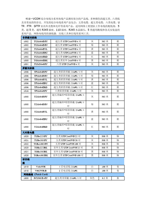
唯康--VCOM综合布线全系列布线产品拥有很全的产品线,多种颜色的超五类、六类线及非常高的性价比。
开发的综合布线系列产品包含:五类电缆,超五类电缆,六类电缆,U TP,FTP,SFTP室内外光缆和光纤等系列产品,适用网络工程团队工作布线的配线架,5类,超5类,通用RJ45插座,110插座,RJ45水晶插头;5类通用跳线和各式安装盒的
管理渠道非常的严密,价格体系管理完善,给予一定的账期支持,协助代理商及系统集成商提升产品品牌价值和市场份额,现诚招江苏各区域总代、各级代理商、系统集成商,与各级代理商、系统集成商精诚合作共享布线产品市场发展前景。
ProductTypeList-optiMOS(20-250V)

N-Channel MOSFETs: OptiMOS™ (20V…250V) Product TypeProduct TypeBSN045NE2LSBSN011NE2LSBSN011NE2LSIBSN012N03LSBSN012N03LSIBSN048N03LSBSB012NE2LXBSB014N04LX3 GBSB015N04NX3 GBSB017N03LX3 GBSB012N03LX3 GBSB028N06NN3 GBSB044N08NN3 GBSB056N10NN3 GBSB013NE2LXIBSB008NE2LXBSB280N15NZ3 G BSB165N15NZ3 G BSB012NE2LXI BSF024N03LT3 G BSF050N03LQ3 G BSF030NE2LQ BSF134N10NJ3 G BSF110N06NT3 G BSF450NE7NH3 G BSF035NE2LQ IPB015N04L G IPB027N10N3 G IPB035N08N3 G IPB015N04N G IPB019N06L3 G IPB083N10N3 G IPB042N10N3 G IPB054N06N3 GIPB037N06N3 G IPB097N08N3 G IPB055N03L G IPB054N08N3 G IPB042N03L G IPB022N04L G IPB065N03L G IPB072N15N3 G IPB025N08N3 G IPB080N03L G IPB081N06L3 G IPB147N03L G IPB096N03L G IPB136N08N3 GIPB090N06N3 G IPB029N06N3 G IPB049NE7N3 G IPB031NE7N3 G IPB020NE7N3 G IPB123N10N3 G IPB038N12N3 G IPB144N12N3 G IPB320N20N3 G IPB107N20N3 G IPB200N25N3 G IPB600N25N3 G BUZ32 H3045A BUZ31 H3045A IPB108N15N3 G BUZ30A H3045AIPB107N20NA IPB057N06N IPB026N06N IPB230N06L3 G IPB067N08N3 G IPB034N03L G IPB009N03L G IPB011N04L G IPB011N04N G IPB016N06L3 G IPB017N06N3 G IPB019N08N3 G IPB020N04N G IPB025N10N3 G IPB030N08N3 GIPB036N12N3 G IPB065N15N3 G IPB010N06NIPB014N06NSPD07N20 GIPD031N06L3 G IPD034N06N3 G IPD035N06L3 G IPD036N04L GIPD038N06N3 G IPD048N06L3 G IPD053N08N3 G SPD50N03S2L-06 G SPD30N03S2L-07 G IPD068N10N3 G SPD50N03S2-07 GIPD082N10N3 G IPD088N06N3 G IPD096N08N3 G SPD30N03S2L-10 G IPD127N06L GIPD135N08N3 G IPD160N04L GIPD170N04N GIPD200N15N3 G SPD30N03S2L-20 G IPD220N06L3 G IPD25CN10N GIPD250N06N3 G IPD33CN10N GIPD350N06L GIPD640N06L G IPD78CN10N G IPD800N06N G IPD122N10N3 G IPD180N10N3 G IPD110N12N3 G IPD031N03L G IPD040N03L G IPD050N03L G IPD060N03L G IPD075N03L G IPD090N03L G IPD320N20N3 G IPD600N25N3 G IPD530N15N3 G IPD105N03L G IPD135N03L GIPD025N06N IPD053N06N IPI023NE7N3 G IPI034NE7N3 G IPI052NE7N3 G IPI126N10N3 G IPI180N10N3 G IPI041N12N3 G IPI076N12N3 G IPI147N12N3 G IPI045N10N3 G IPI086N10N3 G IPI030N10N3 G IPI04CN10N G IPI072N10N3 G IPI26CN10N G IPI35CN10N GIPI075N15N3 G IPI200N15N3 G IPI024N06N3 G IPI032N06N3 G IPI040N06N3 G IPI037N08N3 G IPI320N20N3 G IPI110N20N3 G IPI200N25N3 G IPI600N25N3 G IPI111N15N3 G IPI530N15N3 G IPI020N06NIPI029N06N BUZ31 H3046 IPI084N06L3 GIPU135N08N3 G IPS110N12N3 G IPS060N03L G IPS075N03L G IPS031N03L G IPS040N03L G IPS090N03L G IPS105N03L G IPS135N03L G IPS050N03L G BSZ0908ND BSZ0907ND BSC0921NDI BSC0923NDI BSC0924NDI BSC0925ND BSC0910NDI BSC0911NDBSZ035N03LS G BSZ035N03MS G BSZ040N04LS G BSZ042N04NS G BSZ050N03LS G BSZ050N03MS G BSZ058N03LS G BSZ058N03MS G BSZ067N06LS3 G BSZ076N06NS3 G BSZ088N03MS G BSZ088N03LS G BSZ097N04LS G BSZ100N06LS3 G BSZ100N03MS GBSZ105N04NS G BSZ110N06NS3 G BSZ123N08NS3 G BSZ130N03MS G BSZ130N03LS G BSZ165N04NS G BSZ340N08NS3 G BSZ440N10NS3 G BSZ160N10NS3 G BSZ900N15NS3 G BSZ520N15NS3 G BSZ0909NSBSZ240N12NS3 G BSZ12DN20NS3 G BSZ16DN25NS3 GBSZ42DN25NS3 G BSZ900N20NS3 G BSZ060NE2LS BSZ065N03LS BSZ036NE2LS BSZ018NE2LS BSZ0901NSBSZ0901NSIBSZ0902NSBSZ0904NSIBSZ0902NSIBSZ018NE2LSI BSZ042N06NS BSZ023N04LS BSZ150N10LS3 G BSO615N GBSO033N03MS GBSO083N03MS G BSO110N03MS G BSO330N02K G BSO150N03MD G BSO220N03MD G BSC010NE2LS BSC050NE2LS BSC046N02KS G BSC019N02KS G BSC014N03LS G BSC016N03LS G BSC014N03MS G BSC016N04LS G BSC016N03MS G BSC017N04NS G BSC018N04LS GBSC020N03MS G BSC020N03LS G BSC025N03MS G BSC027N04LS G BSC025N03LS G BSC028N06LS3 G BSC030N03MS G BSC030N04NS G BSC030N03LS G BSC031N06NS3 G BSC034N03LS G BSC035N04LS G BSC042N03MS G BSC042N03LS GBSC050N03MS G BSC050N04LS G BSC050N03LS G BSC054N04NS G BSC057N03MS G BSC057N03LS G BSC057N08NS3 G BSC059N04LS G BSC060N10NS3 G BSC067N06LS3 G BSC076N06NS3 G BSC079N10NS GBSC080N03LS G BSC082N10LS G BSC090N03MS G BSC090N03LS G BSC093N04LS G BSC100N03MS G BSC100N10NSF G BSC100N06LS3 G BSC105N10LSF G BSC110N06NS3 G BSC118N10NS G BSC120N03MS G BSC120N03LS GBSC123N10LS G BSC152N10NSF G BSC190N15NS3 G BSC159N10LSF G BSC196N10NS G BSC205N10LS G BSC252N10NSF G BSC265N10LSF G BSC340N08NS3 G BSC042NE7NS3 G BSC160N10NS3 G BSC440N10NS3 G BSC077N12NS3 G BSC190N12NS3 G BSC520N15NS3 GBSC600N25NS3 G BSC026N02KS G BSC070N10NS3 G BSC109N10NS3 G BSC0909NSBSC360N15NS3 G BSC0908NSBSC240N12NS3 G BSC900N20NS3 G BSC12DN20NS3 G BSC16DN25NS3 G BSC22DN20NS3 G BSC018NE2LS BSC024NE2LS BSC011N03LS BSC052N03LSBSC0902NSBSC032NE2LS BSC0901NSIBSC0904NSIBSC010NE2LSI BSC0902NSIBSC014NE2LSI BSC018NE2LSI BSC011N03LSI BSC0906NSBSC009NE2LS BSC036NE7NS3 G BSC046N10NS3 G BSC028N06NS BSC010N04LSI BSC014N04LS BSC014N04LSIBSC039N06NS BSC014N06NS BSC010N04LS BSC500N20NS3 G BSC022N04LS BSC072N03LD G BSC150N03LD G BSC750N10ND G IPP023NE7N3 G IPP034NE7N3 G IPP052NE7N3 G BUZ31L HBUZ73 HBUZ73A HBUZ73AL HBUZ73L HIPP180N10N3 G IPP041N12N3 G IPP048N12N3 G IPP076N12N3 G IPP114N12N3 G IPP147N12N3 G IPP030N10N3 G IPP045N10N3 G IPP04CN10N G IPP05CN10N G IPP072N10N3 G IPP086N10N3 G IPP12CN10L G IPP16CN10N G IPP075N15N3 G IPP200N15N3 G IPP034N03L GIPP055N03L G IPP065N03L G IPP080N03L G IPP096N03L G IPP114N03L G IPP015N04N G IPP023N04N G IPP039N04L G IPP041N04N G IPP024N06N3 G IPP032N06N3 G IPP037N06L3 G IPP040N06N3 G IPP052N06L3 G IPP057N06N3 G IPP084N06L3 G IPP093N06N3 GIPP028N08N3 G IPP037N08N3 G IPP057N08N3 G IPP070N08N3 G IPP100N08N3 G IPP139N08N3 G IPP320N20N3 G IPP110N20N3 G IPP200N25N3 G IPP600N25N3 G BUZ31 HBUZ32 HIPP111N15N3 G BUZ30A HIPP065N04N G IPP530N15N3 GIPP048N04N G IPP110N20NA IPP147N03L G IPP029N06N IPP020N06N IPP040N06N IPP060N06N IPA028N08N3 G IPA037N08N3 G IPA057N08N3 G IPA100N08N3 G IPA045N10N3 G IPA086N10N3 G IPA126N10N3 G IPA180N10N3 G IPA030N10N3 GIPA105N15N3 G IPA032N06N3 G IPA057N06N3 G IPA093N06N3 G IPT004N03L IPT007N06N IPT020N10N3 IPT059N15N3Datasheet Group Product Status /dgdl/BSN045NE2LS_rev1.0.pdf?fBlade 3x3 (USON-6)in production olderId=db3a304313b8b5a60113cee8763b02d7&fileId=db3a30433d68e984013d7ca959855780/dgdl/BSN011NE2LS_rev1.3.pdf?fBlade 3x3 (USON-6)in production olderId=db3a304313b8b5a60113cee8763b02d7&fileId=db3a30433d68e984013d7cbfeef05815Blade 3x3 (USON-6)in production /dgdl/BSN011NE2LSI_rev1.3.pdf?folderId=db3a304313b8b5a60113cee8763b02d7&fileId=db3a30433d68e984013d7ccf22ee58e4Blade 3x3 (USON-6)in production /dgdl/BSN012N03LS_rev1.3.pdf?folderId=db3a304313b8b5a60113cee8763b02d7&fileId=db3a30433d68e984013d7cde510c594c/dgdl/BSN012N03LSI_rev1.3.pdf?Blade 3x3 (USON-6)in production folderId=db3a304313b8b5a60113cee8763b02d7&fileId=db3a30433d68e984013d7cea5f8559f4Blade 3x3 (USON-6)in production /dgdl/BSN048N03LS_rev1.0.pdf?folderId=db3a304313b8b5a60113cee8763b02d7&fileId=db3a30433d68e984013d7cf6d2e25a60/dgdl/BSB012NE2LX_Rev+2.3.pdfCanPAK™ M-size in production?folderId=db3a304326dfb1300126fb3bec803f1a&fileId=db3a304326dfb1300126fb6a32613f3dCanPAK™ M-size in production /dgdl/BSB014N04LX3+G_Rev+2.3.pdf?folderId=db3a304313b8b5a60113cee8763b02d7&fileId=db3a304320d39d590121a02c6c737a9bCanPAK™ M-size in production /dgdl/BSB015N04NX3+G_Rev+2.4.pdf?folderId=db3a304313b8b5a60113cee8763b02d7&fileId=db3a304320d39d590121a03bbfcd7aacCanPAK™ M-size in production /dgdl/BSB017N03LX3+G_Rev+2.2.pdf?folderId=db3a304313b8b5a60113cee8763b02d7&fileId=db3a304320d39d590121a04b132c7abb/dgdl/BSB012N03LX3+G_Rev_+2CanPAK™ M-size in production.1_pdf.pdf?folderId=db3a304313b8b5a60113cee8763b02d7&fileId=db3a304320d39d590121a0112ce07a8b/dgdl/BSB028N06NN3_G_rev2.0.CanPAK™ M-size in production pdf?folderId=db3a30431441fb5d01148ca9f1be0e77&fileId=db3a30432e25b009012e29fda4e23838/dgdl/BSB044N08NN3_G_rev2.0.CanPAK™ M-size in production pdf?folderId=db3a304313b8b5a60113cee8763b02d7&fileId=db3a30435819ae2e012e385cde7b70d4CanPAK™ M-size in production /dgdl/BSB056N10NN3+G_Rev+2.5.pdf?folderId=db3a304313b8b5a60113cee8763b02d7&fileId=db3a30442e152e91012e390b9a631459/dgdl/BSB013NE2LXI_Rev+2.3.pdCanPAK™ M-size in production f?folderId=db3a304313b8b5a60113cee8763b02d7&fileId=db3a30432e398416012e47a158802577/dgdl/BSB008NE2LX_Rev+1.3.pdfCanPAK™ M-size in production?folderId=db3a304313b8b5a60113cee8763b02d7&fileId=db3a30432e564707012e5745ca7d000eCanPAK™ M-size in production /dgdl/BSB280N15NZ3+G+Rev+2.5_.pdf?folderId=db3a304326623792012669f6bee2224b&fileId=db3a30432e779412012e7b0b544c3852CanPAK™ M-size in production /dgdl/BSB165N15NZ3+G+Rev+2.2.pdf?folderId=db3a304326623792012669f6bee2224b&fileId=db3a30432e779412012e7b04a1353843/dgdl/BSB012NE2LXI_rev1+1.pdfCanPAK™ M-size coming soon?folderId=db3a304313b8b5a60113cee8763b02d7&fileId=db3a30433f764301013f805e3eb247c1CanPAK™ S-size in production /dgdl/BSF024N03LT3+G_Rev+2.1_pdf.pdf?folderId=db3a30431ddc9372011ebafa04517f8b&fileId=db3a30432239cccd012282adaadf7bc8CanPAK™ S-size in production /dgdl/BSF050N03LQ3+G_Rev+2.2.pdf?folderId=db3a304313b8b5a60113cee8763b02d7&fileId=db3a304320d39d590121a0f584407b1cCanPAK™ S-size in production /dgdl/BSF030NE2LQ_Rev+2.3.pdf?folderId=db3a304313b8b5a60113cee8763b02d7&fileId=db3a30432e398416012e47a8f0792588/dgdl/BSF134N10NJ3+G_Rev+2.5CanPAK™ S-size in production.pdf?folderId=db3a304313b8b5a60113cee8763b02d7&fileId=db3a30432e779412012e7afa4a6c3834CanPAK™ S-size in production /dgdl/BSF110N06NT3_G_rev2.0.pdf?folderId=db3a304313b8b5a60113cee8763b02d7&fileId=db3a3043382e837301387b92fdc80c37CanPAK™ S-size in production /dgdl/BSF450NE7NH3G_rev2.0.pdf?folderId=db3a304313b8b5a60113cee8763b02d7&fileId=db3a30433a047ba0013a687e2ae403daCanPAK™ S-size coming soon /dgdl/BSF035NE2LQ_rev1+1.pdf?folderId=db3a304313b8b5a60113cee8763b02d7&fileId=db3a30433f764301013f7fe8a925463cD2PAK (TO-263)in production /dgdl/IPB015N04L_rev1.2.pdf?folderId=db3a304313b8b5a60113cee8763b02d7&fileId=db3a30431936bc4b0119382488c359d3D2PAK (TO-263)in production /dgdl/IPB027N10N3+G_Rev2.4.pdf?folderId=db3a304313b8b5a60113cee8763b02d7&fileId=db3a30431ce5fb52011d1ed9348e15efD2PAK (TO-263)in production /dgdl/IPP037N08N3_Rev2.3.pdf?folderId=db3a304313b8b5a60113cee8763b02d7&fileId=db3a30431add1d95011ae8426111565bD2PAK (TO-263)in production /dgdl/IPB015N04N_rev2.2.pdf?folderId=db3a3043156fd5730115c7d50620107c&fileId=db3a30431689f4420116c474de8f0845/dgdl/IPB019N06L3_Rev2.2.pdf?fD2PAK (TO-263)in production olderId=db3a30431441fb5d01148ca9f1be0e77&fileId=db3a30431ddc9372011e2600a49e467b/dgdl/IPP086N10N3+G_Rev2.5.pdD2PAK (TO-263)in productionf?folderId=db3a304313b8b5a60113cee8763b02d7&fileId=db3a30431ce5fb52011d1ac5c8fa1358/dgdl/IPP045N10N3+G_Rev2.5.pdD2PAK (TO-263)in productionf?folderId=db3a304313b8b5a60113cee8763b02d7&fileId=db3a30431ce5fb52011d1e8b0cc31586D2PAK (TO-263)not for new design /dgdl/IPP_B057N06N3_Rev2.2.pdf?folderId=db3a30431441fb5d01148ca9f1be0e77&fileId=db3a30431ddc9372011e2b439f1d4d93/dgdl/IPP037N06L3_Rev2.7.pdf?fD2PAK (TO-263)in production olderId=db3a304313b8b5a60113cee8763b02d7&fileId=db3a30431b3e89eb011b4561341f7d38D2PAK (TO-263)in production /dgdl/IPP040N06N3_Rev1.03.pdf?folderId=db3a3043163797a6011637c252b10018&fileId=db3a304317a7483601182c2d4f447647D2PAK (TO-263)in production /dgdl/IPP_I_B100N08N3_Rev2.2.pdf?folderId=db3a304313b8b5a60113cee8763b02d7&fileId=db3a30431ddc9372011e071f53b82619D2PAK (TO-263)in production /dgdl/IPP055N03L_rev2.0.pdf?folderId=db3a30431441fb5d01148c401f250e27&fileId=db3a30431441fb5d01148d01ee1c0e91/dgdl/IPP057N08N3_Rev1.2.pdf?fD2PAK (TO-263)in production olderId=db3a304313b8b5a60113cee8763b02d7&fileId=db3a304317a748360117cf0cf5951d06/dgdl/IPP042N03L_rev2.0.pdf?foldD2PAK (TO-263)in production erId=db3a30431441fb5d01148c401f250e27&fileId=db3a30431441fb5d01148d012d010e8eD2PAK (TO-263)discontinued /dgdl/IPB022N04L_rev2.0.pdf?folderId=db3a304313b8b5a60113cee8763b02d7&fileId=db3a30431936bc4b01193836c99c5a08D2PAK (TO-263)in production /dgdl/IPP065N03L_rev2.0.pdf?folderId=db3a30431441fb5d01148c401f250e27&fileId=db3a30431441fb5d011492371ebc0fe2/dgdl/IPP075N15N3+G_Rev2.06.pD2PAK (TO-263)in production df?folderId=db3a304313b8b5a60113cee7c66a02d6&fileId=db3a304319c6f18c0119cd76cc527ab6/dgdl/IPB025N08N3_Rev1.2.pdf?fD2PAK (TO-263)in production olderId=db3a304313b8b5a60113cee8763b02d7&fileId=db3a304317a748360117d35658bc066bD2PAK (TO-263)in production /dgdl/IPP080N03L_rev2.0.pdf?folderId=db3a30431441fb5d01148c401f250e27&fileId=db3a30431441fb5d01148d028c300e94D2PAK (TO-263)in production /dgdl/IPP_B084N06L3_Rev2.23.pdf?folderId=db3a304313b8b5a60113cee8763b02d7&fileId=db3a30431b3e89eb011b4592273f7db2/dgdl/IPP147N03L_rev2.0.pdf?foldD2PAK (TO-263)in production erId=db3a30431441fb5d01148c401f250e27&fileId=db3a30431441fb5d01148d08f1f30e9aD2PAK (TO-263)in production /dgdl/IPP096N03L_rev2.0.pdf?folderId=db3a30431441fb5d01148c401f250e27&fileId=db3a30431441fb5d01148d0849910e97/dgdl/IPP139N08N3_Rev2.5.pdf?fD2PAK (TO-263)in production olderId=db3a304313b8b5a60113cee8763b02d7&fileId=db3a30431add1d95011ae8a77e3656c2?folderId=db3a304313b8b5a60113cee7c66a02d6&fileId=db3a304319c6f18c0119cd1cc23279beD2PAK (TO-263)in production /dgdl/IPP_B093N06N3_Rev1.2.pdf?folderId=db3a3043163797a6011637c252b10018&fileId=db3a304317a7483601182c3043a67656D2PAK (TO-263)in production /dgdl/IPP032N06N3_Rev2.2.pdf?folderId=db3a30431441fb5d01148ca9f1be0e77&fileId=db3a30431ddc9372011e2a84ff084cc8/dgdl/IPB049NE7N3_Rev2.2.pdf?fD2PAK (TO-263)in production olderId=db3a304313b8b5a60113cee8763b02d7&fileId=db3a304320d39d590121a517a48e0bb9D2PAK (TO-263)in production /dgdl/IPB031NE7N3_Rev2.2.pdf?folderId=db3a304313b8b5a60113cee8763b02d7&fileId=db3a304320d39d590121a52a87680bc8/dgdl/IPB020NE7N3_Rev2.2.pdf?fD2PAK (TO-263)in production olderId=db3a304313b8b5a60113cee8763b02d7&fileId=db3a304320d39d590121e31c838554d3D2PAK (TO-263)in production /dgdl/IPP126N10N3+G_Rev2.3.pdf?folderId=db3a304313b8b5a60113cee8763b02d7&fileId=db3a30432239cccd012260508e027f74D2PAK (TO-263)in production /dgdl/IPP_I_B041N12N3_Rev2.2.pdf?folderId=db3a304313b8b5a60113cee8763b02d7&fileId=db3a30432239cccd0122a75b86467ca4D2PAK (TO-263)in production /dgdl/IPP_I_B147N12N3+G_Rev2.6.pdf?folderId=db3a304313b8b5a60113cee8763b02d7&fileId=db3a30432239cccd0122a79a30f57d01D2PAK (TO-263)in production /dgdl/IPP_B_I_320N20N3+G+Rev2.3.pdf?folderId=db3a3043163797a6011637d4bae7003b&fileId=db3a3043243b5f170124967064ba184aD2PAK (TO-263)in production /dgdl/IPP_I_110N20N3+G_IPB107N20N3+G+Rev2.3.pdf?folderId=db3a3043163797a6011637d4bae7003b&fileId=db3a3043243b5f170124968e7d1f18e7/dgdl/IPP_B_I_200N25N3+G+RevD2PAK (TO-263)in production2.4.pdf?folderId=db3a3043163797a6011637d4bae7003b&fileId=db3a3043243b5f17012496b87e9f1971/dgdl/IPP_B_600N25N3+G+Rev2.D2PAK (TO-263)in production3.pdf?folderId=db3a3043163797a6011637d4bae7003b&fileId=db3a3043243b5f17012496c9548d199cD2PAK (TO-263)not for new design /dgdl/BUZ32+H3045A+rev+2.2.pdf?folderId=db3a304325305e6d012596c6ca7b290a&fileId=db3a304325305e6d01259718c8d8291eD2PAK (TO-263)not for new design /dgdl/BUZ31+H3045+A+Rev+2.1.pdf?folderId=db3a304325305e6d012596c6ca7b290a&fileId=db3a304325305e6d0125971c90292922D2PAK (TO-263)in production /dgdl/IPP_I111N15N3+G_IPB108N15N3+G_Rev2.1.pdf?folderId=db3a304325305e6d01254a567c041b4e&fileId=db3a304325305e6d01254a5795541b4fD2PAK (TO-263)in production /dgdl/Buz30a+H3045A+Rev+2.2.pdf?folderId=db3a304325305e6d012596c6ca7b290a&fileId=db3a304325305e6d012596cd45e4290folderId=db3a304326623792012669f6bee2224b&fileId=db3a30432662379201266a1f6dd2227c/dgdl/IPP110N20NA_IPB107N20NA+Rev2.1.pdf?folderId=db3a304325305e6d012596c6ca7b290a&fileId=db3a3043300464130130307ce52a20a3D2PAK (TO-263)in production/dgdl/IPB057N06N_Rev2.2.pdf?folderId=db3a304313b8b5a60113cee8763b02d7&fileId=db3a30433727a44301372c2ed50b49b3D2PAK (TO-263)in production/dgdl/IPB026N06N_Rev2.2.pdf?folderId=db3a304313b8b5a60113cee8763b02d7&fileId=db3a3043372d5cc8013754c7b2a74f7cD2PAK (TO-263)in production/dgdl/IPP_B230N06L3_Rev2.2_.pdf?folderId=db3a30431441fb5d01148ca9f1be0e77&fileId=db3a30431ddc9372011e2aab4a564d14D2PAK (TO-263)discontinued/dgdl/IPP070N08N3_Rev2.3.pdf?folderId=db3a304313b8b5a60113cee8763b02d7&fileId=db3a30431add1d95011ae849e8f1566bD2PAK (TO-263)in production/dgdl/IPP034N03L_rev2.0.pdf?folderId=db3a304313b8b5a60113cee8ed2a02db&fileId=db3a304313b8b5a60113d3c9730503e7D2PAK (TO-263)in production/dgdl/IPB009N03L_rev1.3.pdf?fold erId=db3a3043156fd5730115c7d50620107c&fileId=db3a3 0431689f4420116d426b6770ca3D2PAK 7pin (TO-2637pin)in production/dgdl/IPB011N04L_rev1.3.pdf?fold erId=db3a3043156fd5730115c7d50620107c&fileId=db3a3 0431689f4420116c451f4e20825D2PAK 7pin (TO-2637pin)in production/dgdl/IPB011N04N_rev1+4.pdf?fol derId=db3a3043163797a6011643468e7505a4&fileId=db3 a3043163797a601164373e07005f8D2PAK 7pin (TO-2637pin)in production/dgdl/IPB016N06L3_Rev2.3.pdf?f olderId=db3a30431441fb5d01148ca9f1be0e77&fileId=db3 a30431ddc9372011e261543e54693D2PAK 7pin (TO-2637pin)in production/dgdl/IPB017N06N3_Rev2.2.pdf?f olderId=db3a30431441fb5d01148ca9f1be0e77&fileId=db3 a30431ddc9372011e264a7ab746ea D2PAK 7pin (TO-2637pin)in production/dgdl/IPB019N08N3_Rev2.3.pdf?f olderId=db3a304313b8b5a60113cee8763b02d7&fileId=db 3a30431add1d95011ae87fdf90569f D2PAK 7pin (TO-2637pin)in production/dgdl/IPB020N04N_rev1.3.pdf?fol derId=db3a304313b8b5a60113cee8763b02d7&fileId=db3 a30431936bc4b0119382c70a859ed D2PAK 7pin (TO-2637pin)in production/dgdl/IPB025N10N3+G_Rev2.03.p df?folderId=db3a304313b8b5a60113cee8763b02d7&fileId =db3a30431ce5fb52011d1ab1d9d51349D2PAK 7pin (TO-2637pin)in production/dgdl/IPB030N08N3_Rev2.3.pdf?f olderId=db3a304313b8b5a60113cee8763b02d7&fileId=db 3a30431add1d95011ae88a47a856b1D2PAK 7pin (TO-2637pin)in productiondf?folderId=db3a304313b8b5a60113cee8763b02d7&fileId=db3a30431ce5fb52011d1ed1fd3915e07pin)/dgdl/IPB036N12N3+G_Rev2.2.pd f?folderId=db3a304313b8b5a60113cee8763b02d7&fileId= db3a304323b87bc20123c7030ed51f56D2PAK 7pin (TO-2637pin)in production/dgdl/IPB065N15N3+G_Rev2.1.pd f?folderId=db3a304326623792012669f6bee2224b&fileId= db3a30432662379201266a0379d1225c D2PAK 7pin (TO-2637pin)in production/dgdl/IPB010N06N_Rev2.1.pdf?fol derId=db3a304313b8b5a60113cee8763b02d7&fileId=db3 a3043353fdc1601355341f17a485f D2PAK 7pin (TO-2637pin)in production/dgdl/IPB014N06N_Rev2.2.pdf?fol derId=db3a304313b8b5a60113cee8763b02d7&fileId=db3 a3043353fdc160135534e951e4873D2PAK 7pin (TO-2637pin)in production/dgdl/spd07n20_Rev+2.5.pdf?folderId=db3a30431a5c32f2011a809773886508&fileId=db3a30431f848401011fc73c3e60796aDPAK (TO-252)in production/dgdl/IPD031N06L3_Rev2.0.pdf?folderId=db3a30431441fb5d01148ca9f1be0e77&fileId=db3a30431ddc9372011e2a9f6a9d4d02DPAK (TO-252)in production/dgdl/IPD034N06N3_Rev2.0.pdf?folderId=db3a30431441fb5d01148ca9f1be0e77&fileId=db3a30431ddc9372011e2a97343b4cf3DPAK (TO-252)in production/dgdl/IPD035N06L3_Rev2.3.pdf?folderId=db3a304313b8b5a60113cee8763b02d7&fileId=db3a30431b3e89eb011b4558ed7f7d14DPAK (TO-252)in production/dgdl/IPD036N04L_rev1.0.pdf?folderId=db3a3043163797a6011643468e7505a4&fileId=db3a3043163797a6011643476a6505a5DPAK (TO-252)in production/dgdl/IPD038N06N3_Rev1.02.pdf?folderId=db3a3043132679fb0113346bdc4505a3&fileId=db3a304317a7483601181bf8dae11675DPAK (TO-252)in production/dgdl/IPD048N06L3_Rev2.0.pdf?folderId=db3a30431441fb5d01148ca9f1be0e77&fileId=db3a30431ddc9372011e2b4f496e4db0DPAK (TO-252)in production/dgdl/IPD053N08N3_Rev1.0.pdf?folderId=db3a304313b8b5a60113cee8763b02d7&fileId=db3a304317a748360117cf072cf31ce8DPAK (TO-252)in production/dgdl/SPD50N03S2L-06+rev+1.2.pdf?folderId=db3a304313b8b5a60113cee8763b02d7&fileId=db3a30431b3e89eb011b9718a1a20e3cDPAK (TO-252)in production/dgdl/SPD30N03S2L-07+rev+1.2.pdf?folderId=db3a304313b8b5a60113cee8763b02d7&fileId=db3a30431b3e89eb011b92c6dcba0f89DPAK (TO-252)in production/dgdl/IPD068N10N3+G_Rev2.1.pdf?folderId=db3a304313b8b5a60113cee8763b02d7&fileId=db3a30431ce5fb52011d1eb7aeb615d1DPAK (TO-252)in production/dgdl/SPD50N03S2-07+rev+1.2.pdf?folderId=db3a304313b8b5a60113cee8763b02d7&fileId=db3a30431b3e89eb011b97117df80e2aDPAK (TO-252)in productionolderId=db3a30431441fb5d01148ca9f1be0e77&fileId=db3a30431ddc9372011e2b5528634dc0DPAK (TO-252)in production /dgdl/IPP086N10N3+G_Rev2.5.pdf?folderId=db3a304313b8b5a60113cee8763b02d7&fileId=db3a30431ce5fb52011d1ac5c8fa1358DPAK (TO-252)in production /dgdl/IPD088N06N3_Rev2.0.pdf?folderId=db3a30431441fb5d01148ca9f1be0e77&fileId=db3a30431ddc9372011e2b2351db4d5c/dgdl/IPD096N08N3_Rev2+1.pdf?DPAK (TO-252)in production folderId=db3a304313b8b5a60113cee8763b02d7&fileId=db3a30431ce5fb52011d1f35150315feDPAK (TO-252)in production /dgdl/SPD30N03S2L-10+rev+1.2.pdf?folderId=db3a304313b8b5a60113cee8763b02d7&fileId=db3a30431b3e89eb011b96e752ea0e08/dgdl/IPD127N06LG%2BRev1.2.pDPAK (TO-252)not for new design df?folderId=db3a30431a5c32f2011a809773886508&fileId=db3a30431f848401011fc786d4077a24DPAK (TO-252)in production /dgdl/IPD135N08N3_Rev2.1.pdf?folderId=db3a304313b8b5a60113cee8763b02d7&fileId=db3a30431add1d95011ae8b1143256d4/dgdl/IPD160N04L_rev1.0.pdf?folDPAK (TO-252)not for new design derId=db3a3043163797a6011643468e7505a4&fileId=db3a3043163797a60116436401cf05cfDPAK (TO-252)not for new design /dgdl/IPD170N04N_rev1.0.pdf?folderId=db3a3043163797a6011643468e7505a4&fileId=db3a3043163797a601164367820f05dd/dgdl/IPD200N15N3_Rev2.05.pdfDPAK (TO-252)in production?folderId=db3a304313b8b5a60113cee7c66a02d6&fileId=db3a304319c6f18c0119cd1cc23279beDPAK (TO-252)in production /dgdl/SPD30N03S2L-20+rev+1.2.pdf?folderId=db3a304313b8b5a60113cee8763b02d7&fileId=db3a30431b3e89eb011b96f227b90e19/dgdl/IPD220N06L3_Rev2.0.pdf?fDPAK (TO-252)not for new design olderId=db3a30431441fb5d01148ca9f1be0e77&fileId=db3a30431ddc9372011e266fb35e471aDPAK (TO-252)in production /dgdl/IPP26CN10N_Rev1.08.pdf?folderId=db3a304412b407950112b408e8c90004&fileId=db3a304412b407950112b42b420244aa/dgdl/IPD250N06N3_Rev2.0.pdf?fDPAK (TO-252)not for new design olderId=db3a30431441fb5d01148ca9f1be0e77&fileId=db3a30431ddc9372011e268ceca1474fDPAK (TO-252)in production /dgdl/IPP35CN10N_Rev1.09.pdf?folderId=db3a304412b407950112b408e8c90004&fileId=db3a304412b407950112b42b457b44b1DPAK (TO-252)in production /dgdl/IPD350N06L+G++Rev1.3.pdf?folderId=db3a304313b8b5a60113cee8763b02d7&fileId=db3a30431be39b97011c320778777982?folderId=db3a304313b8b5a60113cee8763b02d7&fileId=db3a30431be39b97011c31db9a4f795cDPAK (TO-252)in production /dgdl/IPD640N06L%2BG%2BRev1.4.pdf?folderId=db3a30431ddc9372011ebafa04517f8b&fileId=db3a30431f848401011fcafb4ac00440DPAK (TO-252)in production /dgdl/IPP80CN10N_Rev1.09.pdf?folderId=db3a304412b407950112b408e8c90004&fileId=db3a304412b407950112b42c2aaf468dDPAK (TO-252)not for new design /dgdl/IPD800N06N%2BG%2BRev1.3.pdf?folderId=db3a30431ddc9372011ebafa04517f8b&fileId=db3a30431f848401011fcaff7887044fDPAK (TO-252)in production /dgdl/IPD122N10N3+G_Rev2.2.pdf?folderId=db3a304313b8b5a60113cee8763b02d7&fileId=db3a30432239cccd0122604a0b2e7f65DPAK (TO-252)in production /dgdl/IPD180N10N3+G_Rev2.2.pdf?folderId=db3a304313b8b5a60113cee8763b02d7&fileId=db3a30432239cccd01226070a4bb7fb9DPAK (TO-252)in production /dgdl/IPD_S110N12N3+G_Rev2.2.pdf?folderId=db3a304313b8b5a60113cee8763b02d7&fileId=db3a30432239cccd0122a7a49e2b7d1dDPAK (TO-252)in production /dgdl/IPD031N03L_rev2+1.pdf?folderId=db3a304313b8b5a60113cee8763b02d7&fileId=db3a30432313ff5e01239e2ed62a6fffDPAK (TO-252)in production /dgdl/IPD040N03LG_rev1%5B1%5D.02.pdf?folderId=db3a304313b8b5a60113cee8763b02d7&fileId=db3a30432313ff5e01239e343d7c700fDPAK (TO-252)in production /dgdl/IPD050N03LG_rev1%5B1%5D.02.pdf?folderId=db3a304313b8b5a60113cee8763b02d7&fileId=db3a30432313ff5e01239e47dbfe701f/dgdl/IPD060N03LG_rev2.0.pdf?fDPAK (TO-252)in production olderId=db3a304313b8b5a60113cee8763b02d7&fileId=db3a30432313ff5e01239e4d33a3702f/dgdl/IPD075N03LG_rev1%5B1%DPAK (TO-252)in production5D.1.pdf?folderId=db3a304313b8b5a60113cee8763b02d7&fileId=db3a30432313ff5e01239e56990c7047/dgdl/IPD090N03LG_rev2.0_.pdf?DPAK (TO-252)in production folderId=db3a304313b8b5a60113cee8763b02d7&fileId=db3a30432313ff5e01239eac54cb707bDPAK (TO-252)in production /dgdl/IPD320N20N3+G+Rev2.3.pdf?folderId=db3a3043163797a6011637d4bae7003b&fileId=db3a3043243b5f1701249669796017f3/dgdl/IPD600N25N3+G+Rev2.3.pDPAK (TO-252)in productiondf?folderId=db3a3043163797a6011637d4bae7003b&fileId=db3a3043243b5f17012496b03c67195bDPAK (TO-252)in production /dgdl/IPD530N15N3_Rev2.5.pdf?folderId=db3a304326623792012669f6bee2224b&fileId=db3a30432662379201266a1f6dd2227c/dgdl/IPD105N03LG_rev2.1.pdf?fDPAK (TO-252)in production olderId=db3a304313b8b5a60113cee8ed2a02db&fileId=db3a3043271faefd0127b84794a33348/dgdl/IPD135N03LG_rev2.1.pdf?fDPAK (TO-252)in production olderId=db3a304313b8b5a60113cee8ed2a02db&fileId=db3a304327b897500127b8b9540f0003DPAK (TO-252)not for new design /dgdl/IPP12CN10N_Rev1.07.pdf?folderId=db3a304412b407950112b408e8c90004&fileId=db3a304412b407950112b42c236e467cDPAK (TO-252)in production /dgdl/IPD025N06N_Rev2.3.pdf?folderId=db3a304313b8b5a60113cee8763b02d7&fileId=db3a304336415dec0136531648062c76/dgdl/IPD053N06N_Rev2.2.pdf?foDPAK (TO-252)in production lderId=db3a304313b8b5a60113cee8763b02d7&fileId=db3a30433727a44301372c22c4c3499fI2PAK (TO-262)in production /dgdl/IPP_I023NE7N3_Rev2+11.pdf?folderId=db3a304313b8b5a60113cee8763b02d7&fileId=db3a304320d39d5901210a9da8c22702I2PAK (TO-262)in production /dgdl/IPP_I034NE7N3_Rev2+01.pdf?folderId=db3a304313b8b5a60113cee8763b02d7&fileId=db3a304320d39d5901210ab6d74b2720I2PAK (TO-262)in production /dgdl/IPP_I052NE7N3_Rev2+01.pdf?folderId=db3a304313b8b5a60113cee8763b02d7&fileId=db3a304320d39d5901210ac80a8c273d/dgdl/IPP126N10N3+G_Rev2.3.pdI2PAK (TO-262)in productionf?folderId=db3a304313b8b5a60113cee8763b02d7&fileId=db3a30432239cccd012260508e027f74I2PAK (TO-262)in production /dgdl/IPP180N10N3+G+Rev2.2.pdf?folderId=db3a304313b8b5a60113cee8763b02d7&fileId=db3a30432239cccd01226066faa07f9dI2PAK (TO-262)in production /dgdl/IPP_I_B041N12N3_Rev2.2.pdf?folderId=db3a304313b8b5a60113cee8763b02d7&fileId=db3a30432239cccd0122a75b86467ca4I2PAK (TO-262)in production /dgdl/IPP_I076N12N3+G_Rev2.3.pdf?folderId=db3a304313b8b5a60113cee8763b02d7&fileId=db3a30432239cccd0122a77a83ab7cd4I2PAK (TO-262)in production /dgdl/IPP_I_B147N12N3+G_Rev2.6.pdf?folderId=db3a304313b8b5a60113cee8763b02d7&fileId=db3a30432239cccd0122a79a30f57d01I2PAK (TO-262)in production /dgdl/IPP045N10N3+G_Rev2.5.pdf?folderId=db3a304313b8b5a60113cee8763b02d7&fileId=db3a30431ce5fb52011d1e8b0cc31586I2PAK (TO-262)in production /dgdl/IPP086N10N3+G_Rev2.5.pdf?folderId=db3a304313b8b5a60113cee8763b02d7&fileId=db3a30431ce5fb52011d1ac5c8fa1358I2PAK (TO-262)in production /dgdl/IPP030N10N3+G_Rev2%5B1%5D.1.pdf?folderId=db3a304313b8b5a60113cee8763b02d7&fileId=db3a30432313ff5e0123939fdbcf03c9/dgdl/IPP04CN10N_Rev1.4.pdf?foI2PAK (TO-262)not for new design lderId=db3a304313b8b5a60113cee8763b02d7&fileId=db3a30432313ff5e012393a80d1d03d8/dgdl/IPP072N10N3+G_Rev2%5BI2PAK (TO-262)in production1%5D.1.pdf?folderId=db3a304313b8b5a60113cee8763b02d7&fileId=db3a30432313ff5e012393bed2d20405/dgdl/IPP26CN10N_Rev1.08.pdf?fI2PAK (TO-262)discontinued olderId=db3a304313b8b5a60113cee8763b02d7&fileId=db3a30432313ff5e012393d285660441I2PAK (TO-262)discontinued /dgdl/IPP35CN10N_Rev1.09.pdf?folderId=db3a304313b8b5a60113cee8763b02d7&fileId=db3a304317a748360117cf1876cc1d1a。
VFS6045型产品特性说明书

VFS6045SA102VFS6045SA151VFS6045SA451VFS6045VA031VFS6045VA102 VFS6045VA121VFS6045VA201VFS6045VA301E M C C o m p o n e n t sNoise suppression filterFor home appliances (conductive noise countermeasure) VFS seriesVFS6045 typeFEATURESAPPLICATIONPART NUMBER CONSTRUCTIONCHARACTERISTICS SPECIFICATION TABLEMeasurement equipmentEquivalent measurement equipment may be used.VFS6045V A031Series nameL×W×H dimensions V: at 10MHzS: at 1MHzInternal codeImpedance6.0×6.0×4.5 mm(Ω)Type Impedance DC resistance Rated current Part No.(Ω)Typ.(Ω)Min.(Ω)typ.(Ω)max.(A)max.6045VA[at 10MHz]57300.0120.0156 6.0VFS6045VA0311451200.0190.0247 5.1VFS6045VA1212422000.0230.0299 4.95VFS6045VA2014683000.0360.0468 3.6VFS6045VA301127510000.0750.0975 2.5VFS6045VA102 6045SA[at 1MHz]1881500.1750.2275 1.5VFS6045SA1515524500.470.6110.9VFS6045SA45112321000 1.15 1.4950.5VFS6045SA102Measurement item Product No.ManufacturerImpedance4294A Keysight T echnologiesDC resistance34420A Hewlett-PackardE M C C o m p o n e n t sVFS6045 typeZ FREQUENCY CHARACTERISTICSINSERTION LOSS VS. FREQUENCY CHARACTERISTICSE M C C o m p o n e n t s VFS6045 typeSHAPE & DIMENSIONSRECOMMENDED LAND PATTERNRECOMMENDED REFLOW PROFILEPACKAGING STYLETEMPERATURE RANGE, INDIVIDUAL WEIGHT *Operating temperature range includes self-temperature rise.**The storage temperature range is for after the assembly.Dimensions in mmDimensions in mmT ype A B KVFS6045 6.3 6.3 4.7Package quantity1500 pcs/reelOperating temperature range*Storagetemperature range**Individualweight–40 to +105 °C–40 to +105 °C0.6 gE M C C o m p o n e n t sREMINDERS FOR USING THESE PRODUCTSBefore using these products, be sure to request the delivery specifications.SAFETY REMINDERSPlease pay sufficient attention to the warnings for safe designing when using this products.The storage period is less than 12 months. Be sure to follow the storage conditions (temperature: 5 to 30°C, humidity: 10 to 75% RH or less).If the storage period elapses, the soldering of the terminal electrodes may deteriorate.Do not use or store in locations where there are conditions such as gas corrosion (salt, acid, alkali, etc.).Before soldering, be sure to preheat components.The preheating temperature should be set so that the temperature difference between the solder temperature and chip temperature does not exceed 150°C.Soldering corrections after mounting should be within the range of the conditions determined in the specifications.If overheated, a short circuit, performance deterioration, or lifespan shortening may occur.When embedding a printed circuit board where a chip is mounted to a set, be sure that residual stress is not given to the chip due to the overall distortion of the printed circuit board and partial distortion such as at screw tightening portions.Self heating (temperature increase) occurs when the power is turned ON, so the tolerance should be sufficient for the set thermal design.Carefully lay out the coil for the circuit board design of the non-magnetic shield type.A malfunction may occur due to magnetic interference.Use a wrist band to discharge static electricity in your body through the grounding wire.Do not expose the products to magnets or magnetic fields.Do not use for a purpose outside of the contents regulated in the delivery specifications.The products listed on this catalog are intended for use in general electronic equipment (AV equipment, telecommunications equip-ment, home appliances, amusement equipment, computer equipment, personal equipment, office equipment, measurement equip-ment, industrial robots) under a normal operation and use condition.The products are not designed or warranted to meet the requirements of the applications listed below, whose performance and/or qual-ity require a more stringent level of safety or reliability, or whose failure, malfunction or trouble could cause serious damage to society,person or property.If you intend to use the products in the applications listed below or if you have special requirements exceeding the range or conditions set forth in the each catalog, please contact us.(1) Aerospace/aviation equipment(2) T ransportation equipment (cars, electric trains, ships, etc.)(3) Medical equipment(4) Power-generation control equipment (5) Atomic energy-related equipment (6) Seabed equipment(7) T ransportation control equipment(8) Public information-processing equipment (9) Military equipment(10) Electric heating apparatus, burning equipment (11) Disaster prevention/crime prevention equipment(12) Safety equipment(13) Other applications that are not considered general-purposeapplicationsWhen designing your equipment even for general-purpose applications, you are kindly requested to take into consideration securing pro-tection circuit/device or providing backup circuits in your equipment.REMINDERSVFS6045SA102VFS6045SA151VFS6045SA451VFS6045VA031VFS6045VA102 VFS6045VA121VFS6045VA201VFS6045VA301。
ES030-5中文资料(Powerbox)中文数据手册「EasyDatasheet - 矽搜」
过载防护护
Yes
温度系数 环境
CV: 5x10 /°C, CC: 10x10/°C.
选型表
工作温度 储存温度 湿度
降额 冷却 热防护护
-20°C至+ 50°C -40°C至+ 85°C 最大. 95%RH,无冷凝,最高可达40℃. 最大. 75%RH,无冷凝,最高可达50℃. 50°C以上,减免线性至20%@ 75℃
.
技术指标
INPUT
电压范围
浪涌电流
功率因数
AC 90-265V,为48Hz-到62Hz 10A与NTC电阻30Ω抗寒性. 0.99 / 0.83(110 / 230V交流)
操作
效率
83-84%
阻抗
ES015-10: 100mΩ, ES030-5: 200mΩ, ES075-
2: 250mΩ,ES0300-0.45: 5Ω.
ES0300-0.45: 0.3mA. 线,90-265VAC
EMC标准
ES015-10: 0.5mA, ES030-5: 0.2mA, ES075-2: 0.1mA,EMI标准
ES0300-0.45: 0.05mA. 电压/电流调整到10圈电位器,分辨率0.03%
纹波和噪声峰 - 峰值
见表格
过压防护护 (固定)
ES015-10: 18V, ES030-5: 40V, ES075-2: 90V, ES0300-0.45: 330V.
机械 安装
Case 尺寸/重量
短路防护护
Yes
No 是,主/从操作可能 是,总电压不超过600V 电压0-5V
XBS104S14资料

0.6
10000
FoFrowrawradrdVoVltolatgage:e VFV(FV()V)
Reverse Current: IR (ЖA) Reverse Current IR (uA)
1000
VR=40V
20V
IF=1A
0.4
5V
100
0.5A
10
0.2
0.1A
1
0.01A
0.0
-50
0
50
20
30
40
ReRveevresreseVoVltoaltgaeg:eV RV(RV()V)
0.5
0.0 0
50
100
150
Opeeraattinngg TTeemmppeerraattuurree : Ta (ˆ℃)
2/3
XBS104S14
1. The products and product specifications contained herein are subject to change without notice to improve performance characteristics. Consult us, or our representatives before use, to confirm that the information in this catalog is up to date.
XBS104S14
Schottky Barrier Diode, 1A, 40V, SOD-123A Package
ETR1609-002
˙FEATURES
Forward Voltageç ç ç ç ç ç Forward Currentç ç ç ç ç ç
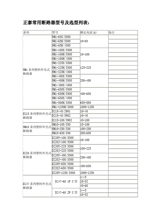
正泰常用断路器选型手册
DW16-2500A
2500
DW16-3200A
3200
DW16-4000A
4000
DW17系列万能式断路器
DW17-630A
630
电动(快速)固定垂直
DW17-1000A
1000
DW17-1250A
1250
DW17-1600A
1600
DW17-2000A
2000
DW17-2500A
2500
NM1-225H/4300
NM1-400S/3300
250-400
NM1-400H/3300
NM1-400S/4300
NM1-630S/3300
400-630
NM1-630H/3300
NM1-630S/4300
NM1-800H/3300
630-800
NM1-1250H/3300
1000-1250
DZ15系列塑料外壳式断路器
16-100
DZ20J-100/3300
DZ20Y-225/3300
100-225
DZ20J-225/3300
DZ20Y-400/3300
250-400
DZ20J-400/3300
DZ20Y-630/3300
400-630
DZ20J-630/3300
DZ20Y-1250/3300
1000-1250
DZ47系列塑料外壳式断路器
100-250
DZ20LE-400/3N300
200-400
DZ20LE-630/3N300
400-630
DZ20LE系列漏电断路器
DZ267LE-32
6-32
DZ47LE系列漏电断路器
MAX3045BESE+中文资料

General DescriptionThe MAX3040–MAX3045 is a family of 5V quad RS-485/RS-422 transmitters designed for digital data trans-mission over twisted-pair balanced lines. All transmitter outputs are protected to ±10kV using the Human Body Model. In addition the MAX3040–MAX3045 withstand ±4kV per IEC 1000-4-4 Electrical Fast Transient/Burst Stressing. The MAX3040/MAX3043 (250kbps) and the MAX3041/MAX3044 (2.5Mbps) are slew-rate limited transmitters that minimize EMI and reduce reflections caused by improperly terminated cables, thus allowing error-free transmission.The MAX3040–MAX3045 feature a hot-swap capability*that eliminates false transitions on the data cable during power-up or hot insertion. The MAX3042B/MAX3045B are optimized for data transfer rates up to 20Mbps, the MAX3041/MAX3044 for data rates up to 2.5Mbps, and the MAX3040/MAX3043 for data rates up to 250kbps.The MAX3040–MAX3045 offer optimum performance when used with the MAX3093E or MAX3095 5V quad differential line receivers or MAX3094E/MAX3096 3V quad differential line receivers.The MAX3040–MAX3045 are ESD-protected pin-compat-ible, low-power upgrades to the industry-standard ‘SN75174 and ‘DS26LS31C. They are available in space-saving TSSOP, narrow SO, and wide SO packages.*Patent pendingApplicationsTelecommunications Equipment Industrial Motor ControlTransmitter for ESD-Sensitive Applications Hand-Held Equipment Industrial PLCs NetworkingFeatureso ESD Protection: ±10kV—Human Body Model o Single +5V Operationo Guaranteed Device-to-Device Skew(MAX3040/MAX3041/MAX3043/MAX3044)o Pin-Compatible with ‘SN75174, ‘26LS31C and LTC487o Hot-Swappable for Telecom Applications o Up to 20Mbps Data Rate (MAX3042B/MAX3045B)o Slew-Rate Limited (Data Rates at 2.5Mbps and 250kbps)o 2nA Low-Power Shutdown Mode o 1mA Operating Supply Currento ±4kV EFT Fast Transient Burst Immunity per IEC 1000-4-4o Level 2 Surge Immunity per IEC 1000-4-5,Unshielded Cable Model o Ultra-Small 16-Pin TSSOP, 16-Pin Narrow SO, and Wide 16-Pin SOMAX3040–MAX3045±10kV ESD-Protected, Quad 5V RS-485/RS-422Transmitters________________________________________________________________Maxim Integrated Products1Pin ConfigurationsSelector GuideOrdering Information19-2143; Rev 1; 12/01Ordering Information continued at end of data sheet.For pricing, delivery, and ordering information,please contact Maxim/Dallas Direct!at 1-888-629-4642, or visit Maxim’s website at .M A X 3040–M A X 3045±10kV ESD-Protected, Quad 5V RS-485/RS-422TransmittersABSOLUTE MAXIMUM RATINGSELECTRICAL CHARACTERISTICSStresses beyond those listed under “Absolute Maximum Ratings” may cause permanent damage to the device. These are stress ratings only, and functional operation of the device at these or any other conditions beyond those indicated in the operational sections of the specifications is not implied. Exposure to absolute maximum rating conditions for extended periods may affect device reliability.All voltages referenced to ground (GND).Supply Voltage (V CC ).............................................................+7V Control Input Voltage (EN, EN , EN_) .........-0.3V to (V CC + 0.3V)Driver Input Voltage (T_IN).........................-0.3V to (V CC + 0.3V)Driver Output Voltage (Y_, Z_)(Driver Disabled).............................................-7.5V to +12.5V Driver Output Voltage (Y_, Z_)(Driver Enabled).................................................-7.5V to +10V Continuous Power Dissipation (T A = +70°C)16-Pin TSSOP (derate 9.4mW/°C above +70°C)..........755mW16-Pin Narrow SO (derate 8.70mW/°C above +70°C)..696mW 16-Pin Wide SO (derate 9.52mW/°C above +70°C).....762mW Operating Temperature RangeMAX304_C_E.......................................................0°C to +70°C MAX304_E_E....................................................-40°C to +85°C Maximum Junction Temperature.....................................+150°C Storage Temperature Range.............................-65°C to +150°C Lead Temperature (soldering, 10s).................................+300°CMAX3040–MAX3045±10kV ESD-Protected, Quad 5V RS-485/RS-422TransmittersSWITCHING CHARACTERISTICS —MAX3040/MAX3043SWITCHING CHARACTERISTICS —MAX3041/MAX3044M A X 3040–M A X 3045±10kV ESD-Protected, Quad 5V RS-485/RS-422Transmitters 4_______________________________________________________________________________________Note 2:∆V OD and ∆V OC are the changes in V OD and V OC , respectively, when the transmitter input changes state.Note 3:This input current level is for the hot-swap enable (EN_, EN, EN ) inputs and is present until the first transition only. After thefirst transition the input reverts to a standard high-impedance CMOS input with input current I IN . For the first 20µs the input current may be as high as 1mA. During this period the input is disabled.Note 4:Maximum current level applies to peak current just prior to foldback-current limiting. Minimum current level applies duringcurrent limiting.SWITCHING CHARACTERISTICS —MAX3041/MAX3044 (continued)(V CC = +5V ±5%, T A = T MIN to T MAX , unless otherwise noted. Typical values are at V CC = +5V and T A = +25°C.)OUTPUT LOW VOLTAGE (V)O U T P U T C U R R E N T (m A )54-6-5-4-2-1012-3310203040506070800-76OUTPUT CURRENT vs. TRANSMITTEROUTPUT HIGH VOLTAGE0.70.81.00.91.11.220103040506070SUPPLY CURRENT vs. TEMPERATURETEMPERATURE (°C)S U P P L Y C U RR E N T (m A )10010000105152025353040450.1110MAX3040/MAX3043SUPPLY CURRENT vs. DATA RATEDATA RATE (kbps)S U P P L Y C U R R E N T (m A )4000.1110100100010,000MAX3041/MAX3044SUPPLY CURRENT vs. DATA RATEDATA RATE (kbps)S U P P L Y C U R R E N T (m A )1052015353025MAX3042B/MAX3045BSUPPLY CURRENT vs. DATA RATEDATA RATE (kbps)0.1100100010,000110100,000S U P P L Y C U R R E N T (m A )60010203050400201040306050700426810OUTPUT CURRENT vs. TRANSMITTEROUTPUT LOW VOLTAGEOUTPUT LOW VOLTAGE (V)O U T P U T C U R R E N T (m A )MAX3040–MAX3045±10kV ESD-Protected, Quad 5V RS-485/RS-422Transmitters_______________________________________________________________________________________5Typical Operating Characteristics(V CC = +5V, T A = +25°C, unless otherwise noted.)020104030605070021345OUTPUT CURRENTvs. DIFFERENTIAL OUTPUT VOLTAGEM A X 3040 t oc 07DIFFERENTIAL OUTPUT VOLTAGE (V)O U T P U T C U R R E N T (m A )2.102.202.152.352.302.252.502.452.402.5520301040506070TRANSMITTER DIFFERENTIAL OUTPUTVOLTAGE vs. TEMPERATURETEMPERATURE (°C)D I F FE R E N T I A L O U T P U T V O L T A G E (V )M A X 3040–M A X 3045±10kV ESD-Protected, Quad 5V RS-485/RS-422Transmitters 6_______________________________________________________________________________________MAX3040–MAX3045±10kV ESD-Protected, Quad 5V RS-485/RS-422Transmitters7Detailed DescriptionThe MAX3040–MAX3045 are quad RS-485/RS-422 trans-mitters. They operate from a single +5V power supply and are designed to give optimum performance when used with the MAX3093E/MAX3095 5V quad RS-485/RS-422 receivers or MAX3094E/MAX3096 3V quad RS-485/RS-422 receivers. The MAX3040–MAX3045 only need 1mA of operating supply current and consume 2nA when they enter a low-power shutdown mode. The MAX3040–MAX3045 also feature a hot-swap capability allowing line insertion without erroneous data transfer.The MAX3042B/MAX3045B are capable of transferring data up to 20Mbps, the MAX3041/MAX3044 for data rates up to 2.5Mbps, and the MAX3040/MAX3043 for data rates up to 250kbps. All transmitter outputs are pro-tected to ±10kV using the Human Body Model.±10kV ESD ProtectionAs with all Maxim devices, ESD-protection structures are incorporated on all pins to protect against electro-static discharges (ESD) encountered during handling and assembly. The MAX3040–MAX3045 transmitter outputs have extra protection against electrostatic dis-charges found in normal operation. Maxim ’s engineers have developed state-of-the-art structures to protect these pins against the application of ±10kV ESD (Human Body Model), without damage.ESD Test ConditionsESD performance depends on a number of conditions.Contact Maxim for a reliability report that documents test setup, methodology, and results.Human Body ModelFigure 6a shows the Human Body Model, and Figure 6b shows the current waveform it generates when dis-charged into low impedance. This model consists of a 100pF capacitor charged to the ESD voltage of interest,which is then discharged into the device through a 1.5k Ωresistor.Machine ModelThe Machine Model for ESD testing uses a 200pF stor-age capacitor and zero-discharge resistance. It mimics the stress caused by handling during manufacturing and assembly. Of course, all pins (not just RS-485inputs) require this protection during manufacturing.Therefore, the Machine Model is less relevant to the I/O ports than are the Human Body Model.±4kV Electrical Fast Transient/Burst Testing(IEC 1000-4-4)IEC 1000-4-4 Electrical Fast Transient/Burst (EFT/B) is an immunity test for the evaluation of electrical and electronic systems during operating conditions. The test was adapted for evaluation of integrated circuits with power applied. Repetitive fast transients with severe pulsed EMI were applied to signal and control ports. Over 15,000 distinct discharges per minute are sent to each interface port of the IC or equipment under test (EUT) simultaneously with a minimum test duration time of one minute. This simulates stress due to dis-placement current from electrical transients on AC mains, or other telecommunication lines in close prox-imity. Short rise times and very specific repetition rates are essential to the validity of the test.Stress placed on the EUT is severe. In addition to the controlled individual discharges placed on the EUT,extraneous noise and ringing on the transmission line can multiply the number of discharges as well as increase the magnitude of each discharge. All cabling was left unterminated to simulate worst-case reflections.The MAX3040–MAX3045 were setup as specified in IEC 1000-4-4 and the Typical Operating Circuit of this data sheet. The amplitude, pulse rise time, pulse dura-tion, pulse repetition period, burst duration, and burst period (Figure 8)of the burst generator were all verified with a digital oscilloscope according to the specifica-tions in IEC 1000-4-4 sections 6.1.1 and 6.1.2. A simpli-fied diagram of the EFT/B generator is shown in Figure 7. The burst stresses were applied to Y1–Y4 and Z1–Z4simultaneously.IEC 1000-4-4 provides several levels of test severity (see Table 1). The MAX3040–MAX3045 pass the 4000V stress, a special category “X ” beyond the highest level for severe (transient) industrial environments for telecommunication lines.M A X 3040–M A X 3045±10kV ESD-Protected, Quad 5V RS-485/RS-422Transmitters 8_______________________________________________________________________________________MAX3040–MAX3045±10kV ESD-Protected, Quad 5V RS-485/RS-422Transmitters_______________________________________________________________________________________9IEC 1000-4-4 Burst/Electrical FastTransient Test Levels (For Communication Lines)The stresses are applied while the MAX3040–MAX3045are powered up. Test results are reported as:1)Normal performance within the specification limits.2)Temporary degradation or loss of function or perfor-mance which is self-recoverable.3)Temporary degradation, loss of function or perfor-mance requiring operator intervention, such as sys-tem reset.4)Degradation or loss of function not recoverable due to damage.The MAX3040–MAX3045 meets classification 2 listed above. Additionally, the MAX3040–MAX3045 will not latchup during the IEC burst stress events.Hot-Swap CapabilityHot-Swap InputsWhen circuit boards are plugged into a “hot ” back-plane, there can be disturbances to the differential sig-nal levels that could be detected by receivers connected to the transmission line. This erroneous data could cause data errors to an RS-485/RS-422 system.To avoid this, the MAX3040–MAX3045 have hot-swap capable inputs.When a circuit board is plugged into a “hot ” backplane there is an interval during which the processor is going through its power-up sequence. During this time, the processor ’s output drivers are high impedance and will be unable to drive the enable inputs of the MAX3040–MAX3045 (EN, EN , EN_) to defined logic lev-els. Leakage currents from these high impedance dri-vers, of as much as 10µA, could cause the enable inputs of the MAX3040–MAX3045 to drift high or low.Additionally, parasitic capacitance of the circuit board could cause capacitive coupling of the enable inputs to either G ND or V CC . These factors could cause the enable inputs of the MAX3040–MAX3045 to drift to lev-els that may enable the transmitter outputs (Y_ and Z_).To avoid this problem, the hot-swap input provides a method of holding the enable inputs of the MAX3040–MAX3045 in the disabled state as V CC ramps up. This hot-swap input is able to overcome the leakage currents and parasitic capacitances that may pull the enable inputs to the enabled state.Hot-Swap Input CircuitryIn the MAX3040–MAX3045 the enable inputs feature hot-swap capability. At the input there are two NMOSdevices, Q1 and Q2 (Figure 9). When V CC is ramping up from 0, an internal 10µs timer turns on Q2 and sets the SR latch, which also turns on Q1. Transistors Q2, a 700µA current sink, and Q1, an 85µA current sink, pull EN to GND through a 5.6k Ωresistor. Q2 is designed to pull the EN input to the disabled state against an exter-nal parasitic capacitance of up to 100pF that is trying to enable the EN input. After 10µs, the timer turns Q2 off and Q1 remains on, holding the EN input low against three-state output leakages that might enable EN. Q1remains on until an external source overcomes theM A X 3040–M A X 3045required input current. At this time the SR latch resets and Q1 turns off. When Q1 turns off, EN reverts to a standard, high-impedance CMOS input. Whenever V CC drops below 1V, the hot-swap input is reset.The EN12 and EN34 input structures are identical to the EN input. For the EN input, there is a complimentary cir-cuit employing two PMOS devices pulling the EN input to V CC .Hot-Swap Line TransientThe circuit of Figure 10 shows a typical offset termina-tion used to guarantee a greater than 200mV offset when a line is not driven. The 50pF represents the mini-mum parasitic capacitance which would exist in a typi-cal application. In most cases, more capacitance exists in the system and will reduce the magnitude of the glitch. During a “hot-swap ” event when the driver is connected to the line and is powered up, the driver must not cause the differential signal to drop below 200mV. Figures 11 and 12 show the results of the MAX3040–MAX3045 during power-up for two different V CC ramp rates (0.1V/µs and 1V/µs). The photos show the V CC ramp, the single-ended signal on each side of the 100Ωtermination, the differential signal across the termination, and shows the hot-swap line transient stays above the 200mV RS-485 specification.Operation of Enable PinsThe MAX3040–MAX3045 family has two enable-func-tional versions:The MAX3040/MAX3041/MAX3042B have two transmit-ter enable inputs EN12 and EN34. EN12 controls the transmitters 1 and 2, and EN34 controls transmitters 3and 4. EN12 and EN34 are active-high and the part will enter the low-power shutdown mode when both are pulled low. The transmitter outputs are high impedance when disabled (Table 2).The MAX3043/MAX3044/MAX3045B have two transmit-ter enable inputs EN and EN , which are active-high and active-low, respectively. When EN is logic high or EN is logic low all transmitters are active. When EN is pulled low and EN is driven high, all transmitters are disabled and the part enters the low-power shutdown mode. The transmitter outputs are high impedance when disabled (Table 3).Applications InformationTypical ApplicationsThe MAX3040–MAX3045 offer optimum performance when used with the MAX3093E/MAX3095 5V quad receivers or MAX3094E/MAX3096 3V quad differential line receivers. Figure 13 shows a typical RS-485 con-nection for transmitting and receiving data and Figure 14 shows a typical multi-point connection.±10kV ESD-Protected, Quad 5V RS-485/RS-422Transmitters 10______________________________________________________________________________________Figure 9. Simplified Structure of the Driver Enable Pin (EN)MAX3040–MAX3045±10kV ESD-Protected, Quad 5V RS-485/RS-422Transmitters______________________________________________________________________________________11V CC 2V/div Y-Z(20mV/div)238mVY200mV/div Z200mV/div Figure 11. Differential Power-Up Glitch (0.1V/µs)V CC 2V/div Y-Z(5mV/div)238mVY50mV/div Z50mV/div 1µs/divFigure 12. Differential Power-Up Glitch (1V/µs)Figure 10. Differential Power-Up Glitch (Hot Swap)M A X 3040–M A X 3045±10kV ESD-Protected, Quad 5V RS-485/RS-422Transmitters 12______________________________________________________________________________________Typical Multiple-Point ConnectionFigure 14 shows a typical multiple-point connection for the MAX3040–MAX3045 with the MAX3095. Because of the high frequencies and the distances involved, high attention must be paid to transmission-line effects while using termination resistors. A terminating resistor (RT)is simply a resistor that should be placed at the extreme ends of the cable to match the characteristic impedance of the cable. When the termination resis-tance is not the same value as the characteristic impedance of the cable, reflections will occur as the signal is traveling down the cable. Although some reflections are inevitable due to the cable and resistor tolerances, large mismatches can cause significant reflections resulting in errors in the data. With this in mind, it is very important to match the terminating resis-tance and the characteristic impedance as closely as possible. As a general rule in a multi-drop system, termi-nation resistors should always be placed at both ends of the cable.Figure 13. Typical Connection of a Quad Transmitter and a Quad Receiver as a PairMAX3040–MAX3045±10kV ESD-Protected, Quad 5V RS-485/RS-422Transmitters13Pin Configurations (continued)Figure 12. Typical Connection for Multiple-Point RS-485 BusChip InformationTRANSISTOR COUNT: 545PROCESS: CMOSOrdering Information (continued)M A X 3040–M A X 3045±10kV ESD-Protected, Quad 5V RS-485/422Transmitters 14______________________________________________________________________________________Ordering Information (continued)Pin Configurations (continued)MAX3040–MAX3045±10kV ESD-Protected, Quad 5V RS-485/RS-422TransmittersM axim cannot assume responsibility for use of any circuitry other than circuitry entirely embodied in a M axim product. No circuit patent licenses are implied. Maxim reserves the right to change the circuitry and specifications without notice at any time.Maxim Integrated Products, 120 San Gabriel Drive, Sunnyvale, CA 94086 408-737-7600 ____________________15©2001 Maxim Integrated ProductsPrinted USAis a registered trademark of Maxim Integrated Products.Package Information (continued)。
- 1、下载文档前请自行甄别文档内容的完整性,平台不提供额外的编辑、内容补充、找答案等附加服务。
- 2、"仅部分预览"的文档,不可在线预览部分如存在完整性等问题,可反馈申请退款(可完整预览的文档不适用该条件!)。
- 3、如文档侵犯您的权益,请联系客服反馈,我们会尽快为您处理(人工客服工作时间:9:00-18:30)。
SIPMOS Power TransistorProduct Summary Drain source voltage55V DS V Drain-Source on-state resistance Ω0.08R DS(on)I DContinuous drain current13.5AFeatures •N channel•Enhancement mode•Avalanche rated •d v /d t rated•175 ˚C operating temperaturePin 1Pin 2Pin 3GDSPackagingType Package Ordering Code BUZ104S TubeP-TO220-3-1Q67040-S4007-A2BUZ104S E3045A Tape and Reel Q67040-S4007-A6P-TO263-3-2TubeBUZ104S E3045P-TO263-3-2Q67040-S4007-A5Maximum Ratings ,at T j =25˚C, unless otherwise specified ParameterSymbolUnit Value Continuous drain currentT C = 25 ˚C T C = 100 ˚C13.59.6I DAPulsed drain currentT C = 25 ˚CI Dpulse 54Avalanche energy,single pulseI D =13.5A,V DD =25V,R GS =25ΩmJE AS 52Avalanche energy,periodic limited by T jmax 3.5E ARReverse diode d v /d tI S =13.5A,V DS =40V,d i /d t =200A/µs,T jmax = 175 ˚Cd v /d t6kV/µs Gate source voltage V GS ±20V Power dissipationT C = 25 ˚CP tot 35W Operating and storage temperature T j ,T stg˚C-55...+17555/175/56IEC climatic category;DIN IEC 68-1Thermal CharacteristicsParameter ValuesSymbol Unittyp.max.min.CharacteristicsR thJC -- 4.3K/W Thermal resistance, junction - case-Thermal resistance, junction - ambient, leded R thJA-62- ---6240SMD version, device on PCB:@ min. footprint@ 6 cm2 cooling area1)R thJAElectrical Characteristics, at T j = 25 ˚C, unless otherwise specifiedParameter Symbol UnitValuesmin.max.typ.Static CharacteristicsDrain- source breakdown voltage V GS = 0 V, I D = 0.25 mA-V(BR)DSS55-VGate threshold voltage, V GS = V DS I D = 20 µA V GS(th)432.1Zero gate voltage drain currentV DS = 50 V, V GS = 0 V, T j = 25 ˚C V DS = 50 V, V GS = 0 V, T j = 150 ˚C--I DSSµA11000.1-Gate-source leakage current V GS = 20 V, V DS = 0 V I GSS-10nA100Drain-Source on-state resistance V GS = 10 V, I D = 9.6 A R DS(on)-0.0740.08Ω1 Device on 40mm*40mm*1.5mm epoxy PCB FR4 with 6 cm2 (one layer, 70µm thick) copper area for drain connection. PCB is vertical without blown air.Electrical Characteristics, at T j = 25 ˚C, unless otherwise specifiedParameter Symbol Values Unitmin.typ.max. Dynamic CharacteristicsTransconductanceg fs4 5.8-SV DS≥2*I D*R DS(on)max , I D = 9.6 AInput capacitanceC iss-270340pF V GS = 0 V, V DS = 25 V, f = 1 MHzOutput capacitanceC oss-95120V GS = 0 V, V DS = 25 V, f = 1 MHzReverse transfer capacitanceC rss-5065V GS = 0 V, V DS = 25 V, f = 1 MHzTurn-on delay timet d(on)-915ns V DD = 30 V, V GS = 10 V, I D = 13.5 A,R G = 33 ΩRise timet r-2235V DD = 30 V, V GS = 10 V, I D = 13.5 A,R G = 33 ΩTurn-off delay timet d(off)-1830V DD = 30 V, V GS = 10 V, I D = 13.5 A,R G = 33 ΩFall timet f-1725V DD = 30 V, V GS = 10 V, I D = 13.5 A,R G = 33 ΩElectrical Characteristics, at T j = 25 ˚C, unless otherwise specifiedParameter Symbol Values Unitmin.typ.max. Dynamic CharacteristicsGate to source charge V DD = 40 V, I D = 13.5 A3.75nC2.5Q gs-- 3.8Q gdGate to drain chargeV DD = 40 V, I D = 13.5 A5.7Gate charge totalV DD = 40 V, I D = 13.5 A, V GS = 0 to 10 V-9.514 Q gGate plateau voltage V DD = 40 V, I D = 13.5 A V(plateau) 5.9-V-Reverse DiodeInverse diode continuous forward currentT C = 25 ˚CI S--13.5AInverse diode direct current,pulsedT C = 25 ˚CI SM--54Inverse diode forward voltage V GS = 0 V, I F = 27 A V SD- 1.17V1.8Reverse recovery timeV R = 30 V, I F=I S , d i F/d t = 100 A/µs t rr-50ns75Reverse recovery chargeV R = 30 V, I F=l S , d i F/d t = 100 A/µs Q rr-µC0.10.15Power Dissipation P tot = f (T C )20406080100120140160˚C 190T C 0 4 8 12 16 20 24 2832W38 BUZ104SP t o tDrain currentI D = f (T C )parameter: V GS ≥ 10 V20406080100120140160˚C 190T C0 12 3 4 5 6 7 8 9 1011 12A15 BUZ104SI DTransient thermal impedanceZ thJC = f (t p )parameter : D = t p /T10-710-610-510-410-310-210st p-3 10 -210 -110 010 110 K/WBUZ104SZ t h J Csingle pulse0.010.020.050.100.20D = 0.50Safe operating area I D = f (V DS )parameter : D = 0 , T C = 25 ˚C10-110101102V V DS -1 10 010 110 210 ABUZ104SI DR D S (o n ) = V D S / I DDC10 ms1 ms 100 µs10 µst p = 3.3µsTyp. output characteristicsI D = f (V DS )parameter: t p = 80 µs0.01.02.03.04.0V5.5V DS0 4812162024A32 BUZ104SI DV GS [V] aa4.0bb 4.5cc5.0dd5.5ee6.0ff 6.5gg 7.0h h7.5ii 8.0jj 9.0kk10.0lP tot = 35Wl20.0Typ. drain-source-on-resistanceR DS(on) = f (I D )parameter: V GS48121620A 26I D0.000.020.040.060.080.10 0.12 0.14 0.16 0.18 0.200.22 Ω0.26BUZ104SR D S (o n)V GS [V] =c c 5.0d d 5.5e e 6.0f f 6.5g g 7.0h h 7.5ii 8.0j j 9.0kk10.0l l 20.0Typ. transfer characteristics I D = f (V GS )parameter: t p = 80 µsV DS ≥ 2 x I D x R DS(on) max2345678910V12V GS 0 10 20 A40I DTyp. forward transconductanceg fs = f (I D ); T j = 25˚Cparameter: g fs2468101214A 17I D0 12345S7g f sDrain-source on-resistanceR DS(on) = f (T j )parameter : I D= 9.6 A, V GS = 10 V-60-202060100140˚C200T j0.00 0.02 0.04 0.06 0.08 0.10 0.12 0.14 0.16 0.18 0.20 0.220.24 Ω0.28BUZ104SR D S (o n )typ98%Gate threshold voltageV GS(th)= f (T j )parameter : V GS = V DS , I D = 20 µA-60-202060100140˚C200T j0.0 0.4 0.8 1.2 1.6 2.0 2.42.83.2 3.64.04.4V 5.0 V G S (t h )min typmaxTyp. capacitances C = f (V DS )parameter: V GS = 0 V, f = 1 MHz1020V40V DS110 210 310 pFCCissCossCrssForward characteristics of reverse diodeI F = f (V SD )parameter: T j , t p = 80 µs0.00.40.8 1.2 1.6 2.0 2.4V 3.0V SD-110 010 110 210 ABUZ104SI FT j = 25 ˚C typ T j = 25 ˚C (98%)T j = 175 ˚C typ T j = 175 ˚C (98%)Typ. gate chargeV GS = f (Q Gate )parameter: I D puls = 13.5 A24681012nC 15Q Gate0 24681012V16BUZ104SV G SDS maxV 0,8 DS maxV 0,2 Avalanche Energy E AS = f (T j )parameter: I D = 13.5 A, V DD = 25 VR GS = 25 Ω20406080100120140˚C 180T j0 10203040mJ60E A SDrain-source breakdown voltageV (BR)DSS = f (T j )-60-202060100140˚C 200T j50 52 54 56 58 60 62 64V66BUZ104SV (B R )D S S。