IRF7201TRPBF;IRF7201PBF;中文规格书,Datasheet资料
IRLML2244TRPBF;中文规格书,Datasheet资料

1/24/111ORDERING INFORMATION:See detailed ordering and shipping information on the last page of this data sheet.Notes through are on page 10Features and BenefitsBenefitsApplication(s)• System/Load Switchresults in ⇒IRLML2244TRPbFIRLML2244TRPbF 3Fig 2. Typical Output CharacteristicsFig 1. Typical Output CharacteristicsFig 4. Normalized On-ResistanceVs. Temperature-V DS , Drain-to-Source Voltage (V)0.1110100-V DS , Drain-to-Source Voltage (V)-I D , D r a i n -t o -S o u r c e C u r r e n t (A )T J , Junction Temperature (°C)R D S (o n ) , D r a i n -t o -S o u r c e O n R e s i s t a n c eIRLML2244TRPbFFig 6. Typical Gate Charge Vs.Gate-to-Source VoltageFig 5. Typical Capacitance Vs.Drain-to-Source Voltage Fig 8. Maximum Safe Operating AreaFig 7. Typical Source-Drain DiodeForward Voltage110100-V DS , Drain-to-Source Voltage (V)10100100010000C , C a p a c i t a n c e (p F )-V SD , Source-to-Drain Voltage (V)0.1110100-I S D , R e v e r s e D r a i n C u r r e n t (A )110100-V DS , Drain-to-Source Voltage (V)0.010.1110100-I D , D r a i n -t o -S o u r c e C u r r e n t (A)048121620Q G, Total Gate Charge (nC)2468101214-V G S , G a t e -t o -S o u r c e V o l t a g e (V )IRLML2244TRPbF 5Fig 11. Typical Effective Transient Thermal Impedance, Junction-to-AmbientFig 9. Maximum Drain Current Vs.Ambient TemperatureFig 10b. Switching Time WaveformsFig 10a. Switching Time Test Circuit255075100125150T A , Ambient Temperature (°C)012345-I D , D r a i n C u r r e n t (A)t 1 , Rectangular Pulse Duration (sec)R DV DDV DSV t t t tFig 13. Typical On-Resistance Vs. DrainCurrentFig 12. Typical On-Resistance Vs. GateVoltageFig 14b. Gate Charge Test CircuitFig 14a. Basic Gate Charge Waveform 24681012-V GS, Gate -to -Source Voltage (V)20406080100120R D S (o n ), D r a i n -t o -S o u r c e O n R e s i s t a n c e (m Ω)5101520253035-I D , Drain Current (A)04080120160200R D S (o n ), D r a i n -t o -S o u r c e O n R e s i s t a n c e (m Ω)Vgs = -4.5VIdQgs1Qgs2Qgd Qgodr 0 7Fig 15. Typical Threshold Voltage Vs.Junction TemperatureFig 16. Typical Power Vs. TimeT J , Temperature ( °C )-V G S (t h ), G a t e t h r e s h o l d V o l t a g e (V )Time (sec)P o w e r (W )IRLML2244TRPbFMicro3 (SOT-23/TO-236AB) Part Marking InformationMicro3 (SOT-23) Package OutlineDimensions are shown in millimeters (inches)Note: For the most current drawing please refer to IR website at: /package/cF =DA T E C E =X = D =C =B =A =W = (1-26) IF PRECEDED BY LAST DIG IT O F C ALENDA R YEA RH =G =KH G F E D C B 200620032002200520042008200720102009J Y 51292830C B D52ZNote: A line a bove the work we e k(a s s how n he re ) indic a tes Le a d - Fre e.I =J = IRLML2030L = IRLML0060M = IRLML0040K = IRLML0100N = IRLML2060P = IRLML9301R = IRLML9303C u HALOG PAIRLML2244TRPbF 9Micro3™ Tape & Reel InformationDimensions are shown in millimeters (inches)2.05 ( .080 )1.95 ( .077 )TRFEED DIRECTION4.1 ( .161 )3.9 ( .154 )1.6 ( .062 )1.5 ( .060 )1.85 ( .072 )1.65 ( .065 )3.55 ( .139 )3.45 ( .136 )1.1 ( .043 )0.9 ( .036 )4.1 ( .161 )3.9 ( .154 )0.35 ( .013 )0.25 ( .010 )8.3 ( .326 )7.9 ( .312 )1.32 ( .051 )1.12 ( .045 )9.90 ( .390 )8.40 ( .331 )178.00( 7.008 ) MAX.NOTES:1. CONTROLLING DIMENSION : MILLIMETER.2. OUTLINE CONFORMS TO EIA-481 & EIA-541.Note: For the most current drawing please refer to IR website at: /package/IRLML2244TRPbFData and specifications subject to change without notice.IR WORLD HEADQUARTERS: 233 Kansas St., El Segundo, California 90245, USA Tel: (310) 252-7105TAC Fax: (310) 252-7903Visit us at for sales contact information .01/2011Qualification standards can be found at International Rectifier’s web site /product-info/reliabilityHigher qualification ratings may be available should the user have such requirements. Please contact your International Rectifier sales representative for further information: /whoto-call/salesrep/Applicable version of JEDEC standard at the time of product release.Notes:Repetitive rating; pulse width limited by max. junction temperature. Pulse width ≤ 400μs; duty cycle ≤ 2%. Surface mounted on 1 in square Cu board Refer to application note #AN-994.Qualification information †分销商库存信息: IRIRLML2244TRPBF。
IR公司_大功率MOS管选型

I DContinuous Drain Current(A)70°Micro3Surface Mount PackagesV (BR)DSSDrain-to-Source Breakdown Voltage (V)R DS(on)On-State Resistance ()ΩI D Continuous Drain Current 25°C(A)R ΘMax.Thermal Resistance (°C/W)1FaxonDemand Number Case Outline KeyPartNumberPD Max.PowerDissipation (W)N-ChannelLogic LevelIRLML2402*912570.54200.25 1.20.95230H1IRLML2803912580.54300.251.20.93230P-ChannelLogic LevelIRLML6302*912590.54-200.6-0.62-4.8230H1IRLML5103912600.54-300.6-0.61-4.8230* Indicates low VGS(th), which can operate at VGS = 2.7VMeasured at ambient for Micro3, Micro6, Micro8, SO-8, and SOT-223 package styles. All others measured at case.1Micro3SO-8D-PakD -PakSOT-227Micro6SOT-223Micro82 Illustrations not to scaleI DContinuous Drain Current(A)70°Micro6Surface Mount PackagesV (BR)DSSDrain-to-Source Breakdown Voltage (V)R DS(on)On-State Resistance ()ΩI D Continuous Drain Current 25°C(A)R ΘMax.Thermal Resistance (°C/W)1FaxonDemand Number Case Outline KeyPartNumberPD Max.PowerDissipation (W)N-ChannelLogic LevelIRLMS1902915401.7200.10 3.2 2.675H2IRLMS1503915081.7300.103.22.675P-ChannelLogic LevelIRLMS6702*914141.7-200.20-2.3-1.975H2IRLMS5703914131.7-300.20-2.3-1.975* Indicates low VGS(th), which can operate at VGS = 2.7VMeasured at ambient for Micro3, Micro6, Micro8, SO-8, and SOT-223 package styles. All others measured at case.1Micro3SO-8D-PakD -PakSOT-227Micro6SOT-223Micro82 Illustrations not to scaleI DContinuous Drain Current(A)70°Micro8Surface Mount PackagesV (BR)DSSDrain-to-Source Breakdown Voltage (V)R DS(on)On-State Resistance ()ΩI D Continuous Drain Current 25°C(A)R ΘMax.Thermal Resistance (°C/W)1FaxonDemand Number Case Outline KeyPart NumberP D Max.PowerDissipation (W)N-Channel Logic LevelIRF7601* 912611.820 0.035 5.7 4.6 70 H3IRF7603 912621.830 0.035 5.6 4.5 70Dual N-Channel Logic LevelIRF7501* 912651.220 0.135 2.4 1.9 100 H3IRF7503 912661.2530 0.135 2.4 1.9 100P-Channel Logic LevelIRF7604* 912631.8-20 0.09 -3.6 -2.9 70 H3IRF7606 912641.8-30 0.09 -3.6 -2.9 70Dual P-Channel Logic LevelIRF7504* 912671.25-20 0.27 -1.7 -1.4 100 H3IRF7506 912681.25-30 0.27 -1.7 -1.4 100Dual N- and P-Channel Logic LevelIRF7507* 912691.2520 0.1352.4 1.9 100 H3-20 0.27 -1.7 -1.4IRF7509 912701.2530 0.135 2.4 1.9 100-30 0.27 -1.7 -1.4* Indicates low VGS(th), which can operate at VGS = 2.7VMeasured at ambient for Micro3, Micro6, Micro8, SO-8, and SOT-223 package styles. All others measured at case.1Micro3SO-8D-Pak D -PakSOT-227Micro6SOT-223Micro8 2 Illustrations not to scaleI DContinuous Drain Current(A)70°SO-8Surface Mount PackagesV (BR)DSSDrain-to-Source Breakdown Voltage (V)R DS(on)On-State Resistance ()ΩI D Continuous Drain Current 25°C(A)R ΘMax.Thermal Resistance (°C/W)1FaxonDemand Number Case Outline KeyPart Number P D Max.PowerDissipation (W)N-ChannelIRF7413913302.5300.011139.250H4IRF7413A 916132.5300.0135128.450IRF9410915622.5300.0375.850Dual N-ChannelIRF7311914352.0200.029 6.6 5.362.5H4IRF7313914802.0300.029 6.5 5.262.5IRF7333917002.0300.10 3.5 2.862.5917002.0300.050 4.9 3.962.5IRF9956915592.0300.103.52.862.5Dual P-ChannelIRF7314914352.0-200.058-5.3-4.362.5H4IRF7316915052.0-300.058-4.9-3.962.5IRF9953915602.0-300.25-2.3-1.862.5* Indicates low VGS(th), which can operate at VGS = 2.7VMeasured at ambient for Micro3, Micro6, Micro8, SO-8, and SOT-223 package styles. All others measured at case.1Micro3SO-8D-PakD -PakSOT-227Micro6SOT-223Micro82 Illustrations not to scaleI DContinuous Drain Current(A)70°SO-8Surface Mount PackagesV (BR)DSSDrain-to-Source Breakdown Voltage (V)R DS(on)On-State Resistance ()ΩI D Continuous Drain Current 25°C(A)RΘMax.ThermalResistance(°C/W)1FaxonDemand Number Case Outline KeyPart NumberP D Max.PowerDissipation (W)Dual N- and P-ChannelIRF7317 915682.020 0.029 6.6 5.3 62.5 H42.0-20 0.058 -5.3 -4.3 62.5IRF9952 915622.030 0.103.5 2.8 62.5915622.0-30 0.25 -2.3 -1.8 62.5IRF7319 916062.030 0.029 6.5 5.2 62.52.0-30 0.058 -4.9 -3.9 62.5* Indicates low VGS(th), which can operate at VGS = 2.7VMeasured at ambient for Micro3, Micro6, Micro8, SO-8, and SOT-223 package styles. All others measured at case.1Micro3SO-8D-Pak D -PakSOT-227Micro6SOT-223Micro8 2 Illustrations not to scaleI DContinuous Drain Current(A)70°SO-8Surface Mount PackagesV (BR)DSSDrain-to-Source Breakdown Voltage (V)R DS(on)On-State Resistance ()ΩI D Continuous Drain Current 25°C(A)R ΘMax.Thermal Resistance (°C/W)1FaxonDemand Number Case Outline KeyPart Number P D Max.PowerDissipation (W)N-ChannelLogic LevelIRF7401912442.5200.0228.77.050H4IRF7201911002.5300.0307.0 5.650IRF7403912452.5300.0228.55.450Dual N-ChannelLogic LevelIRF7101908712.0200.10 3.5 2.362.5H4IRF7301912382.0200.050 5.2 4.162.5IRF7303912392.0300.050 4.9 3.962.5IRF7103910952.0500.1303.02.362.5P-ChannelLogic LevelIRF7204911032.5-200.060-5.3-4.250H4IRF7404912462.5-200.040-6.7-5.450IRF7205911042.5-300.070-4.6-3.750IRF7406912472.5-300.045-5.8-3.750IRF7416913562.5-300.02-10-7.150* Indicates low VGS(th), which can operate at VGS = 2.7VMeasured at ambient for Micro3, Micro6, Micro8, SO-8, and SOT-223 package styles. All others measured at case.1Micro3SO-8D-PakD -PakSOT-227Micro6SOT-223Micro82 Illustrations not to scaleI DContinuous Drain Current(A)70°SO-8Surface Mount PackagesV (BR)DSSDrain-to-Source Breakdown Voltage (V)R DS(on)On-State Resistance ()ΩI D Continuous Drain Current 25°C(A)R ΘMax.Thermal Resistance (°C/W)1FaxonDemand Number Case Outline KeyPart Number P D Max.PowerDissipation (W)Dual P-ChannelLogic LevelIRF7104910962.0-200.250-2.3-1.862.5H4IRF7304912402.0-200.090-4.3-3.462.5IRF7306912412.0-300.10-3.6-2.962.5Dual N- and P-Channe Logic LevelIRF7307912421.4200.050 4.3 3.490H4-200.090-3.6-2.9IRF7105910972.0250.1093.5 2.862.52-250.25-2.3-1.862IRF7309912432.0300.050 4.9 3.962.5-300.10-3.6-2.9* Indicates low VGS(th), which can operate at VGS = 2.7VMeasured at ambient for Micro3, Micro6, Micro8, SO-8, and SOT-223 package styles. All others measured at case.1Micro3SO-8D-PakD -PakSOT-227Micro6SOT-223Micro82 Illustrations not to scaleI DContinuous Drain Current(A)70°SOT-223Surface Mount PackagesV (BR)DSSDrain-to-Source Breakdown Voltage (V)R DS(on)On-State Resistance ()ΩI D Continuous Drain Current 25°C(A)R ΘMax.Thermal Resistance (°C/W)1FaxonDemand Number Case Outline KeyPart Number P D Max.PowerDissipation (W)N-ChannelIRFL4105913812.1550.045 3.7 3.060H6IRFL110908612.01000.54 1.50.9660IRFL4310913682.11000.20 1.6 1.360IRFL21090868 2.02001.50.960.660IRFL214908622.02502.00.790.560P-ChannelIRFL9110908642.0-1001.2-1.1-0.6960H6N-ChannelLogic LevelIRLL3303913792.1300.031 4.6 3.760H6IRLL014N 914992.1550.14 2.0 1.660IRLL2705913802.1550.043.83.060* Indicates low VGS(th), which can operate at VGS = 2.7VMeasured at ambient for Micro3, Micro6, Micro8, SO-8, and SOT-223 package styles. All others measured at case.1Micro3SO-8D-PakD -PakSOT-227Micro6SOT-223Micro82 Illustrations not to scaleI DContinuous Drain Current(A)100°D-PakSurface Mount PackagesV (BR)DSSDrain-to-Source Breakdown Voltage (V)R DS(on)On-State Resistance ()ΩI D Continuous Drain Current 25°C(A)R ΘMax.Thermal Resistance (°C/W)1FaxonDemand Number Case Outline KeyPart Number P D Max.PowerDissipation (W)N-ChannelIRFR33039164257300.0313321 2.2H7IRFR024N9133638550.0751610 3.3IRFR41059130248550.0452516 2.7IRFR12059131869550.0273723 1.8IRFR11090524251000.54 4.3 2.75IRFR120N 91365391000.219.1 5.8 3.2IRFR391091364521000.11159.5 2.4IRFR2109052625200 1.5 2.6 1.75IRFR22090525422000.8 4.833IRFR21490703252502 2.2 1.45IRFR2249060042250 1.1 3.8 2.43IRFR3109059725400 3.6 1.7 1.15IRFR3209059842400 1.8 3.123IRFR42090599425003 2.4 1.53IRFRC2090637426004.421.33* Indicates low VGS(th), which can operate at VGS = 2.7VMeasured at ambient for Micro3, Micro6, Micro8, SO-8, and SOT-223 package styles. All others measured at case.1Micro3SO-8D-PakD -PakSOT-227Micro6SOT-223Micro82 Illustrations not to scaleI DContinuous Drain Current(A)100°D-PakSurface Mount PackagesV (BR)DSSDrain-to-Source Breakdown Voltage (V)R DS(on)On-State Resistance ()ΩI D Continuous Drain Current 25°C(A)R ΘMax.Thermal Resistance (°C/W)1FaxonDemand Number Case Outline KeyPart Number P D Max.PowerDissipation (W)P-ChannelIRFR55059161057-550.11-18-11 2.2H7IRFR53059140289-550.065-28-18 1.4IRFR90149065425-600.5-5.1-3.25IRFR90249065542-600.28-8.8-5.63IRFR91109051925-100 1.2-3.1-25IRFR91209052042-1000.6-5.6-3.63IRFR9120N 9150739-1000.48-6.5-4.1 3.2IRFR92109052125-2003-1.9-1.25IRFR92209052242-200 1.5-3.6-2.33IRFR92149165850-250 3.0-2.7-1.7 2.5IRFR93109166350-4007.0-1.8-1.12.5* Indicates low VGS(th), which can operate at VGS = 2.7VMeasured at ambient for Micro3, Micro6, Micro8, SO-8, and SOT-223 package styles. All others measured at case.1Micro3SO-8D-PakD -PakSOT-227Micro6SOT-223Micro82 Illustrations not to scaleI DContinuous Drain Current(A)100°D-PakSurface Mount PackagesV (BR)DSSDrain-to-Source Breakdown Voltage (V)R DS(on)On-State Resistance ()ΩI D Continuous Drain Current 25°C(A)R ΘMax.Thermal Resistance (°C/W)1FaxonDemand Number Case Outline KeyPart Number P D Max.PowerDissipation (W)N-ChannelLogic LevelIRLR27039133538300.0452214 3.3H7IRLR33039131657300.0313321 2.2IRLR31039133369300.0194629 1.8IRLR024N 9136338550.0651711 3.3IRLR27059131746550.042415 2.7IRLR29059133469550.0273623 1.8IRLR120N 91541391000.18511 6.9 3.2IRLR341091607521000.10159.52.4* Indicates low VGS(th), which can operate at VGS = 2.7VMeasured at ambient for Micro3, Micro6, Micro8, SO-8, and SOT-223 package styles. All others measured at case.1Micro3SO-8D-PakD -PakSOT-227Micro6SOT-223Micro82 Illustrations not to scaleI DContinuous Drain Current(A)100°D 2PakSurface Mount PackagesV (BR)DSSDrain-to-Source Breakdown Voltage (V)R DS(on)On-State Resistance ()ΩI D Continuous Drain Current 25°C(A)R ΘMax.Thermal Resistance (°C/W)1FaxonDemand Number Case Outline KeyPart NumberP D Max.PowerDissipation (W)N-ChannelIRFZ24NS 913554555 0.07 17 12 3.3 H10IRFZ34NS 913116855 0.04 29 20 2.2IRFZ44NS 9131511055 0.022 49 35 1.4IRFZ46NS 9130512055 0.020 53 37 1.3IRFZ48NS 9140814055 0.016 64 45 1.1IRF1010NS 913723.855 0.011 84 60 40IRF3205S 9130420055 0.008 110 80 0.75IRFZ44ES 9171411060 0.023 48 34 1.4IRF1010ES 9172017060 0.012 83 59 0.90IRF2807S 9151815075 0.013 71 50 1.0IRF520NS 9134047100 0.2 9.5 6.7 3.2IRF530NS 9135263100 0.11 15 11 2.4IRF540NS 91342110100 0.052 27 19 1.6IRF1310NS 91514120100 0.036 36 25 1.3IRF3710S 91310150100 0.028 46 33 1.0IRF3315S 9161794150 0.082 21 15 1.6IRF3415S 91509150150 0.042 37 26 1.0IRFBC20S 9.101450600 4.4 2.2 1.4 2.5IRFBC30S 9101574600 2.2 3.6 2.3 1.7IRFBC40S 91016130600 1.2 6.2 3.9 1.0* Indicates low VGS(th), which can operate at VGS = 2.7VMeasured at ambient for Micro3, Micro6, Micro8, SO-8, and SOT-223 package styles. All others measured at case.1Micro3SO-8D-Pak D -PakSOT-227Micro6SOT-223Micro8 2 Illustrations not to scaleI DContinuous Drain Current(A)100°D 2PakSurface Mount PackagesV (BR)DSSDrain-to-Source Breakdown Voltage (V)R DS(on)On-State Resistance ()ΩI D Continuous Drain Current 25°C(A)R ΘMax.Thermal Resistance (°C/W)1FaxonDemandNumberCase Outline KeyPart NumberP D Max.PowerDissipation (W)IRFBF20S 9166554900 8.0 1.7 1.1 2.3 H10P-ChannelIRF5305S 91386110-55 0.06 -31 -22 1.4 H10IRF4905S 914783.8-55 0.02 -74 -52 40IRF9520NS 9152247-100 0.48 -6.7 -4.8 3.2IRF9530NS 9152375-100 0.20 -14 -9.9 2.0IRF9540NS 9148394-100 0.117 -19 -13 1.6IRF5210S 91405150-100 0.06 -35 -25 1.0* Indicates low VGS(th), which can operate at VGS = 2.7VMeasured at ambient for Micro3, Micro6, Micro8, SO-8, and SOT-223 package styles. All others measured at case.1Micro3SO-8D-Pak D -PakSOT-227Micro6SOT-223Micro8 2 Illustrations not to scaleI DContinuous Drain Current(A)100°D 2PakSurface Mount PackagesV (BR)DSSDrain-to-Source Breakdown Voltage (V)R DS(on)On-State Resistance ()ΩI D Continuous Drain Current 25°C(A)R ΘMax.Thermal Resistance (°C/W)1FaxonDemand Number Case Outline KeyPart NumberP D Max.PowerDissipation (W)N-Channel Logic LevelIRL3302S 916925720 0.020 39 25 2.2 H10IRL3202S916756920 0.016 48 30 1.8IRL3102S 916918920 0.013 61 39 1.4IRL3402S 9169311020 0.01 85 54 1.1IRL3502S 9167614020 0.007 110 67 0.89IRL2703S 913604530 0.04 24 17 3.3IRL3303S 913236830 0.026 38 27 2.2IRL3103S 9133811030 0.014 64 45 1.4IRL2203NS 9136717030 0.007 116 82 0.90IRL3803S 9131920030 0.006 140 98 0.75IRLZ24NS 913584555 0.06 18 13 3.3IRLZ34NS 913086855 0.035 30 21 2.2IRLZ44NS 9134711055 0.022 47 33 1.4IRL3705NS 9150217055 0.01 89 63 0.90IRL2505S 9132620055 0.008 104 74 0.75IRLZ44S 9090615060 0.028 50 36 1.0IRL530NS 9134963100 0.1 15 11 2.4IRL2910S 91376150100 0.026 48 34 1.0* Indicates low VGS(th), which can operate at VGS = 2.7VMeasured at ambient for Micro3, Micro6, Micro8, SO-8, and SOT-223 package styles. All others measured at case.1Micro3SO-8D-Pak D -PakSOT-227Micro6SOT-223Micro8 2 Illustrations not to scaleI DContinuous Drain Current(A)100°SOT-227Surface Mount PackagesV (BR)DSSDrain-to-Source Breakdown Voltage (V)R DS(on)On-State Resistance ()ΩI D Continuous DrainCurrent 25°C(A)RΘMax.Thermal Resistance (°C/W)1FaxonDemand Number Case Outline KeyPart Number P D Max.PowerDissipation (W)N-ChannelFully Isolated Low ChargeFA38SA50LC 916155005000.1338240.25H21FA57SA50LC916506255000.0857360.20* Indicates low VGS(th), which can operate at VGS = 2.7VMeasured at ambient for Micro3, Micro6, Micro8, SO-8, and SOT-223 package styles. All others measured at case.1Micro3SO-8D-PakD -PakSOT-227Micro6SOT-223Micro82 Illustrations not to scaleI DContinuous Drain Current(A)100°I-PakThrough-Hole PackagesV (BR)DSSDrain-to-Source Breakdown Voltage (V)R DS(on)On-State Resistance ()ΩI D Continuous Drain Current 25°C(A)R ΘMax.Thermal Resistance (°C/W)1FaxonDemand Number Case Outline KeyPart Number P D Max.PowerDissipation (W)N-ChannelIRFU33039164257300.0313321 2.2H8IRFU024N 9133638550.0751610 3.3IRFU41059130248550.0452519 2.7IRFU12059131869550.0273723 1.8IRFU11090524251000.54 4.3 2.7 5.0IRFU120N 91365391000.219.1 5.8 3.2IRFU391091364521000.11159.5 2.4IRFU2109052625200 1.5 2.6 1.7 5.0IRFU22090525422000.80 4.8 3.0 3.0IRFU2149070325250 2.0 2.2 1.4 5.0IRFU2249060042250 1.1 3.8 2.4 3.0IRFU3109059725400 3.6 1.7 1.1 5.0IRFU3209059842400 1.8 3.1 2.0 3.0IRFU4209059942500 3.0 2.4 1.5 3.0IRFUC2090637426004.42.01.33.0I-PakTO-220 FullPakTO-262TO-247HEXDIPTO-220AB Illustrations not to scale** Not ratedI DContinuous Drain Current(A)100°I-PakThrough-Hole PackagesV (BR)DSSDrain-to-Source Breakdown Voltage (V)R DS(on)On-State Resistance ()ΩI D Continuous Drain Current 25°C(A)R ΘMax.Thermal Resistance (°C/W)1FaxonDemand Number Case Outline KeyPart Number P D Max.PowerDissipation (W)P-ChannelIRFU55059161057-550.11-18-11 2.2H8IRFU53059140289-550.065-28-18 1.4IRFU90149065425-600.50-5.1-3.2 5.0IRFU90249065542-600.28-8.8-5.6 3.0IRFU91109051925-100 1.2-3.1-2.0 5.0IRFU91209052042-1000.60-5.6-3.6 3.0IRFU9120N 9150739-1000.48-6.5-4.1 3.2IRFU92109052125-200 3.0-1.9-1.2 5.0IRFU92209052242-200 1.5-3.6-2.3 3.0IRFU92149165850-2503.0-2.7-1.7 2.5IRFU93109166350-4007.0-1.8-1.12.5N-ChannelLogic LevelIRLU27039133538300.0452214 3.3H8IRLU33039131657300.0313321 2.2IRLU31039133369300.0194629 1.8IRLU024N 9136338550.0651711 3.3IRLU27059131746550.04241715IRLU29059133469550.0273623 1.8IRLU120N 91541391000.18511 6.9 3.2IRLU341091607521000.10159.52.4I-PakTO-220 FullPakTO-262TO-247HEXDIPTO-220AB Illustrations not to scale** Not ratedI DContinuous Drain Current(A)100°HEXDIPThrough-Hole PackagesV (BR)DSSDrain-to-Source Breakdown Voltage (V)R DS(on)On-State Resistance ()ΩI D Continuous Drain Current 25°C(A)R ΘMax.Thermal Resistance (°C/W)1FaxonDemand Number Case Outline KeyPart Number P D Max.PowerDissipation (W)N-ChannelIRFD014907001.3600.2 1.7 1.2120H9IRFD024906991.3600.1 2.5 1.8120IRFD110903281.31000.54 1.00.71120IRFD120903851.31000.27 1.30.94120IRFD210903861.3200 1.50.60.38120IRFD220904171.32000.80.80.50120IRFD214912711.3250 2.00.570.32120IRFD224912721.3250 1.10.760.43120IRFD310912251.3400 3.60.420.23120IRFD320912261.3400 1.80.600.33120IRFD420912271.3500 3.00.460.26120IRFDC20912281.36004.40.320.21120I-PakTO-220 FullPakTO-262TO-247HEXDIPTO-220AB Illustrations not to scale** Not ratedI D Continuous Drain Current (A)100°TO-220Qg TotalGate Charge(nC)Through-Hole PackagesV (BR)DSSDrain-to-Source Breakdown Voltage (V)R DS(on)On-State Resistance ()ΩI D Continuous Drain Current 25°C (A)R ΘMax.Thermal Resistance(°C/W)1Faxon Demand Number Case OutlineKeyPart Number P D Max.Power Dissipation (W)N-ChannelLow ChargeIRF737LC91314743000.75 6.1** 1.7 3.9H11IRF740LC 910681254000.5510** 1.039IRF840LC 910691255000.858.0** 1.039IRFBC40LC910701256001.26.2**1.039I-PakTO-220 FullPakTO-262TO-247HEXDIPTO-220AB Illustrations not to scale** Not ratedI DContinuous Drain Current(A)100°TO-220ABThrough-Hole PackagesV (BR)DSSDrain-to-Source Breakdown Voltage (V)R DS(on)On-State Resistance ()ΩI D Continuous Drain Current 25°C(A)R ΘMax.Thermal Resistance (°C/W)1FaxonDemand Number Case Outline KeyPart Number P D Max.PowerDissipation (W)N-ChannelIRFZ24N 9135445550.071712 3.3H12IRFZ34N9127656550.042618 2.7IRFZ44N 9130383550.0244129 1.8IRFZ46N 9127788550.024633 1.7IRFZ48N 9140694550.0165337 1.6IRF1010N 91278130550.0127251 1.2IRF320591279150550.0089869 1.0IRFZ34E 9167268600.0422820 2.2IRFZ44E 91671110600.0234834 1.4IRF1010E 91670170600.01281570.90IRF280791517150750.0137150 1.0IRF520N 91339471000.209.5 6.79.5IRF530N 91351601000.111511 2.4IRF540N 91341941000.0522719 1.6IRF1310N 916111201000.0363625 1.3IRF3710913091501000.0284633 1.0IRF331591623941500.0822115 1.6IRF3415914771501500.0423726 1.0IRFBC209062350600 4.4 2.2 1.4 2.5IRFBC309048274600 2.2 3.6 2.3 1.7IRFBC4090506125600 1.2 6.2 3.9 1.0IRFBE2090610548006.51.81.22.3I-PakTO-220 FullPakTO-262TO-247HEXDIPTO-220AB Illustrations not to scale** Not ratedI DContinuous Drain Current(A)100°TO-220ABThrough-Hole PackagesV (BR)DSSDrain-to-Source Breakdown Voltage (V)R DS(on)On-State Resistance ()ΩI D Continuous Drain Current 25°C(A)R ΘMax.Thermal Resistance (°C/W)1FaxonDemand Number Case Outline KeyPart Number P D Max.PowerDissipation (W)IRFBE3090613125800 3.0 4.1 2.6 2.0H12IRFBF3090616125900 3.7 3.6 2.3 1.0IRFBG209060454100011 1.40.86 2.3IRFBG309062012510005.03.12.01.0P-ChannelIRF9Z24N 9148445-550.175-12-8.53.3H12IRF9Z34N 9148556-550.10-17-12 2.7IRF530591385110-550.06-31-22 1.4IRF490591280150-550.02-64-45 1.0IRF9530N 9148275-1000.20-13-9.2 2.0IRF9540N 9143794-1000.117-19-13 1.6IRF521091434150-1000.06-35-25 1.0IRF62159147983-1500.29-11-7.81.8I-PakTO-220 FullPakTO-262TO-247HEXDIPTO-220AB Illustrations not to scale** Not ratedI DContinuous Drain Current(A)100°TO-220ABThrough-Hole PackagesV (BR)DSSDrain-to-Source Breakdown Voltage (V)R DS(on)On-State Resistance ()ΩI D Continuous Drain Current 25°C(A)R ΘMax.Thermal Resistance (°C/W)1FaxonDemand Number Case Outline KeyPart NumberP D Max.PowerDissipation (W)N-Channel Logic LevelIRL3302 916965720 0.020 39 25 2.2 H12IRL3202 916956920 0.016 48 30 1.8IRL3102 916948920 0.013 61 39 1.4IRL3402 9169711020 0.01 85 54 1.1IRL3502 9169814020 0.007 110 67 0.89IRL2703 913594530 0.04 24 17 3.3IRL3303 913225630 0.026 34 24 2.7IRL3103 913378330 0.014 56 40 1.8IRL2203N 9136613030 0.007 100 71 1.230 0.007 61 43 3.2IRL3803 9130115030 0.006 120 83 1.0IRLZ24N 913574555 0.06 18 13 3.3IRLZ34N 913075655 0.035 27 19 2.7IRLZ44N 913468355 0.022 41 29 1.8IRL3705N 9137013055 0.01 77 54 1.2IRL2505 9132520055 0.008 104 74 0.75IRL520N 9149447100 0.18 10 7.1 3.2IRL530N 9134863100 0.10 15 11 2.4IRL540N 9149594100 0.044 30 21 1.6IRL2910 91375150100 0.026 48 34 1.0I-PakTO-220 FullPakTO-262TO-247HEXDIPTO-220AB Illustrations not to scale** Not ratedI D Continuous Drain Current (A)100°TO-220 FullPak (Fully Isolated)Qg TotalGate Charge(nC)Through-Hole PackagesV (BR)DSSDrain-to-Source Breakdown Voltage (V)R DS(on)On-State Resistance ()ΩI D Continuous DrainCurrent 25°C(A)R ΘMax.Thermal Resistance (°C/W)1Fax on Demand Number Case OutlineKeyPart Number P D Max.Power Dissipation (W)N-ChannelLow ChargeIRFI740GLC91209404000.55 6.0** 3.139H13IRFI840GLC 91208405000.85 4.8** 3.139IRFIBC40GLC91211406001.24.0**3.139I-PakTO-220 FullPakTO-262TO-247HEXDIPTO-220AB Illustrations not to scale** Not ratedI DContinuous Drain Current(A)100°TO-220 FullPak (Fully Isolated)Through-Hole PackagesV (BR)DSSDrain-to-Source Breakdown Voltage (V)R DS(on)On-State Resistance ()ΩI D Continuous Drain Current 25°C(A)R ΘMax.Thermal Resistance (°C/W)1FaxonDemand Number Case Outline KeyPart Number P D Max.PowerDissipation (W)N-ChannelIRFIZ24N 9150126550.07139.2 5.8H14IRFIZ34N9148931550.041913 4.8IRFIZ44N 9140338550.02428200.024IRFIZ46N 9130640550.023122 3.8IRFIZ48N 9140742550.0163625 3.6IRFI1010N 9137347550.0124431 3.2IRFI32059137448550.0085640 3.1IRFIZ24E 9167329600.071149.6 5.2IRFIZ34E 9167437600.0422115 4.1IRFI510G 90829271000.54 4.5 3.2 5.5IRFI520N 91362271000.207.2 5.1 5.5IRFI530N 91353331000.11117.8 4.5IRFI540N 91361421000.0521813 3.6IRFI1310N 91611451000.0362216 3.3IRFI371091387481000.0252820 3.1IRFI620G 90832302000.8 4.1 2.6 4.1IRFI630G 90652322000.4 5.9 3.7 3.6IRFI640G 90649402000.189.8 6.2 3.1IRFI614G 9083123250 2.0 2.1 1.3 5.5IRFI624G 9083330250 1.1 3.4 2.2 4.1IRFI634G 90738322500.45 5.6 3.5 3.6IRFI644G 90739402500.287.953.1I-PakTO-220 FullPakTO-262TO-247HEXDIPTO-220AB Illustrations not to scale** Not ratedI DContinuous Drain Current(A)100°TO-220 FullPak (Fully Isolated)Through-Hole PackagesV (BR)DSSDrain-to-Source Breakdown Voltage (V)R DS(on)On-State Resistance ()ΩI D Continuous Drain Current 25°C(A)R ΘMax.Thermal Resistance (°C/W)1FaxonDemand Number Case Outline KeyPart Number P D Max.PowerDissipation (W)IRFI720G 9083430400 1.8 2.6 1.7 4.1H14IRFI730G 9065032400 1.0 3.7 2.3 3.6IRFI740G 90651404000.55 5.4 3.4 3.1IRFI734G 9100135450 1.2 3.4 2.1 3.6IRFI744G 91002404500.63 4.9 3.1 3.1IRFI820G 9064130500 3.0 2.1 1.3 4.1IRFI830G 9064632500 1.5 3.12 3.6IRFI840G 90642405000.85 4.6 2.9 3.1IRFIBC20G 90850306004.41.71.1 4.1IRFIBC30G 90851356002.2 2.5 1.63.6IRFIBC40G 9085240600 1.2 3.5 2.2 3.1IRFIBE20G 9085330800 6.5 1.4.86 4.1IRFIBE30G 9085435800 3.0 2.1 1.4 3.6IRFIBF20G 90855309008.0 1.2.79 4.1IRFIBF30G90856359003.71.91.23.6P-ChannelIRFI9Z24N 9152929-550.175-9.5-6.7 5.2H14IRFI9Z34N 9153037-550.10-14-10 4.1IRFI49059152663-550.02-41-29 2.4IRFI9540G 9083742-1000.117-13-9.2 3.6IRFI9540N 9148742-1000.117-13-9.2 3.6IRFI52109140448-1000.06-20-14 3.1IRFI9634G 9148835-2501.0-4.1-2.63.6I-PakTO-220 FullPakTO-262TO-247HEXDIPTO-220AB Illustrations not to scale** Not ratedI DContinuous Drain Current(A)100°TO-220 FullPak (Fully Isolated)Through-Hole PackagesV (BR)DSSDrain-to-Source Breakdown Voltage (V)R DS(on)On-State Resistance ()ΩI D Continuous Drain Current 25°C(A)R ΘMax.Thermal Resistance (°C/W)1FaxonDemand Number Case Outline KeyPart Number P D Max.PowerDissipation (W)N-ChannelLogic LevelIRLI2203N 9137847300.0076143 3.2H14IRLI38039132048300.0066747 3.1IRLIZ24N 9134426550.06149.9 5.8IRLIZ34N 9132931550.0352014 4.8IRLIZ44N 9149838550.0222820 4.0IRLI3705N 9136947550.014733 3.2IRLI25059132763550.00858412.4IRLI520N 91496271000.187.7 5.4 5.5IRLI530N 91350331000.10117.8 4.5IRLI540N 91497421000.04420143.6IRLI291091384481000.02627193.1P-ChannelLogic LevelIRFI9520G 9083537-1000.6-5.2-3.6 4.1H14IRFI9530G 9083638-1000.03-7.7-5.4 3.6IRFI9620G 9087430-200 1.5-3.0-1.9 4.1IRFI9630G 9083840-2000.8-4.3-2.7 3.6IRFI9640G9083940-2000.5-6.1-3.93.1I-PakTO-220 FullPakTO-262TO-247HEXDIPTO-220AB Illustrations not to scale** Not ratedI D Continuous Drain Current (A)100°TO-247Qg TotalGate Charge(nC)Through-Hole PackagesV (BR)DSSDrain-to-Source Breakdown Voltage (V)R DS(on)On-State Resistance ()ΩI D Continuous Drain Current 25°C (A)R ΘMax.Thermal Resistance (°C/W)1Fax on Demand Number Case OutlineKeyPart Number P D Max.Power Dissipation (W)1N-ChannelLow ChargeIRFP350LC912291904000.3018**0.6570H16IRFP360LC 912302804000.2023**0.4598IRFP450LC 912311905000.4016**0.6570IRFP460LC 912322805000.2720**0.4598IRFPC50LC 912331906000.6013**0.6570IRFPC60LC912342806000.4016**0.4598I-PakTO-220 FullPakTO-262TO-247HEXDIPTO-220AB Illustrations not to scale** Not rated。
SIHF720中文资料
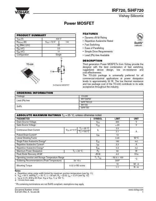
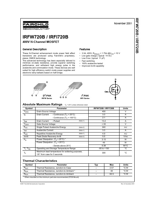
Power MOSFETIRF720, SiHF720Vishay SiliconixFEATURES•Dynamic dV/dt Rating •Repetitive Avalanche Rated •Fast Switching •Ease of Paralleling •Simple Drive Requirements •Lead (Pb)-free AvailableDESCRIPTIONThird generation Power MOSFETs from Vishay provide the designer with the best combination of fast switching,ruggedized device design, low on-resistance and cost-effectiveness.The TO-220 package is universally preferred for all commercial-industrial applications at power dissipation levels to approximately 50 W. The low thermal resistance and low package cost of the TO-220 contribute to its wide acceptance throughout the industry.Notesa.Repetitive rating; pulse width limited by maximum junction temperature (see fig. 11).b.V DD = 50 V, starting T J = 25 °C, L = 30 mH, R G = 25 Ω, I AS = 3.3 A (see fig. 12).c.I SD ≤ 3.3 A, dI/dt ≤ 65 A/µs, V DD ≤ V DS , T J ≤ 150 °C.d. 1.6 mm from case.PRODUCT SUMMARYV DS (V)400 VR DS(on) (Ω)V GS = 10 V1.8Q g (Max.) (nC)20Q gs (nC) 3.3Q gd (nC)11ConfigurationSingleTO-220GD S ORDERING INFORMATIONPackage TO-220Lead (Pb)-free IRF720PbF SiHF720-E3 SnPbIRF720SiHF720ABSOLUTE MAXIMUM RATINGS T C = 25 °C, unless otherwise notedARAMETER SYMBOL LIMIT UNIT Drain-Source Voltage V DS400VGate-Source Voltage V GS ± 20VContinuous Drain Current V GS at 10 VT C = 25 °C I D3.3A T C = 100 °C2.1Pulsed Drain Current a I DM 13Linear Derating Factor0.40W/°C Single Pulse Avalanche Energy b E AS 190mJ Repetitive Avalanche Current a I AR 3.3 A Repetitive Avalanche Energy a E AR 5.0mJ Maximum Power Dissipation T C = 25 °CP D 50WPeak Diode Recovery dV/dt cdV/dt 4.0V/ns Operating Junction and Storage Temperature Range T J , T stg- 55 to + 150°C Soldering Recommendations (Peak Temperature)for 10 s 300d Mounting Torque6-32 or M3 screw10 lbf · in 1.1N · m * Pb containing terminations are not RoHS compliant, exemptions may applyIRF720, SiHF720Vishay SiliconixNotesa.Repetitive rating; pulse width limited by maximum junction temperature (see fig. 11).b.Pulse width ≤ 300 µs; duty cycle ≤ 2 %.THERMAL RESISTANCE RATINGSARAMETER SYMBOL TY.MAX.UNITMaximum Junction-to-Ambient R thJA -62°C/W Case-to-Sink, Flat, Greased Surface R thCS 0.50-Maximum Junction-to-Case (Drain)R thJC- 2.5IRF720, SiHF720Vishay SiliconixCIRF720, SiHF720 Vishay SiliconixIRF720, SiHF720Vishay SiliconixFig. 10a - Switching Time Test CircuitFig. 10b - Switching Time WaveformsFig. 11 - Maximum Effective Transient Thermal Impedance, Junction-to-CaseFig. 12a - Unclamped Inductive Test CircuitFig. 12b - Unclamped Inductive WaveformsIRF720, SiHF720Vishay SiliconixFig. 13a - Basic Gate Charge WaveformFig. 13b - Gate Charge Test CircuitIRF720, SiHF720Vishay Siliconix Array Fig. 14 - For N-ChannelVishay Siliconix maintains worldwide manufacturing capability. Products may be manufactured at one of several qualified locations. Reliability data for Silicon Technology and Package Reliability represent a composite of all qualified locations. For related documents such as package/tape drawings, part marking, andreliability data, see /ppg?91043.Disclaimer Legal Disclaimer NoticeVishayAll product specifications and data are subject to change without notice.Vishay Intertechnology, Inc., its affiliates, agents, and employees, and all persons acting on its or their behalf (collectively, “Vishay”), disclaim any and all liability for any errors, inaccuracies or incompleteness contained herein or in any other disclosure relating to any product.Vishay disclaims any and all liability arising out of the use or application of any product described herein or of any information provided herein to the maximum extent permitted by law. The product specifications do not expand or otherwise modify Vishay’s terms and conditions of purchase, including but not limited to the warranty expressed therein, which apply to these products.No license, express or implied, by estoppel or otherwise, to any intellectual property rights is granted by this document or by any conduct of Vishay.The products shown herein are not designed for use in medical, life-saving, or life-sustaining applications unless otherwise expressly indicated. Customers using or selling Vishay products not expressly indicated for use in such applications do so entirely at their own risk and agree to fully indemnify Vishay for any damages arising or resulting from such use or sale. Please contact authorized Vishay personnel to obtain written terms and conditions regarding products designed for such applications.Product names and markings noted herein may be trademarks of their respective owners.元器件交易网。
IRF8721TRPBF;IRF8721PBF;中文规格书,Datasheet资料
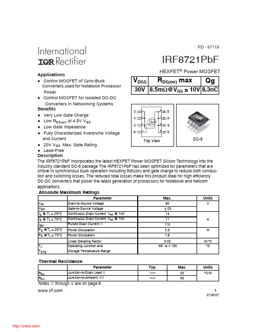
107/30/07IRF8721PbFHEXFET ®Power MOSFETBenefitsl Very Low Gate Charge l Low R DS(on) at 4.5V V GS l Low Gate Impedancel Fully Characterized Avalanche Voltage and Currentl 20V V GS Max. Gate Rating l Lead-Free Applicationsl Control MOSFET of Sync-BuckConverters used for Notebook Processor Powerl Control MOSFET for Isolated DC-DC Converters in Networking Systems SO-8PD - 97119DescriptionThe IRF8721PbF incorporates the latest HEXFET Power MOSFET Silicon Technology into the industry standard SO-8 package The IRF8721PbF has been optimized for parameters that are critical in synchronous buck operation including Rds(on) and gate charge to reduce both conduc-tion and switching losses. The reduced total losses make this product ideal for high efficiency DC-DC converters that power the latest generation of processors for Notebook and Netcom applications.IRF8721PbFStatic @ T = 25°C (unless otherwise specified)IRF8721PbF 3Fig 4. Normalized On-ResistanceVs. TemperatureFig 2. Typical Output CharacteristicsFig 1. Typical Output Characteristics Fig 3. Typical Transfer CharacteristicsV DS , Drain-to-Source Voltage (V)T J , Junction Temperature (°C)R D S (o n ) , D r a i n -t o -S o u r c e O n R e s i s t a n c e(N o r m a l i z e d )V GS , Gate-to-Source Voltage (V)V DS , Drain-to-Source Voltage (V)IRF8721PbFFig 8. Maximum Safe Operating AreaFig 6. Typical Gate Charge Vs.Gate-to-Source VoltageFig 5. Typical Capacitance Vs.Drain-to-Source VoltageFig 7. Typical Source-Drain DiodeForward Voltage110100V DS , Drain-to-Source Voltage (V)100100010000C , C a p a c i t a n c e (p F )0.11101001000I S D , R e v e r s e D r a i n C u r r e n t (A )0.1110100V DS , Drain-to-Source Voltage (V)0.11101001000I D , D r a i n -t o -S o u r c e C u r r e n t (A)510152025Q g , Total Gate Charge (nC)0481216V G S , G a t e -t o -S o u r c e V o l t a g e (V )IRF8721PbF 5Fig 11. Maximum Effective Transient Thermal Impedance, Junction-to-AmbientFig 9. Maximum Drain Current Vs.Case TemperatureFig 10. Threshold Voltage Vs. Temperature255075100125150T A , Ambient Temperature (°C)0481216I D , D r a i n C u r r e n t (A)T J , Temperature ( °C )V G S (t h ) G a t e t h r e s h o l d V o l t a g e (V )t 1, Rectangular Pulse Duration (sec)T h e r m a l R e s p o n s e ( Z t h J A )Fig 13. Maximum Avalanche Energyvs. Drain CurrentFig 12. On-Resistance vs. Gate VoltageFig 15b. Switching Time WaveformsFig 14b. Unclamped Inductive WaveformsFig 14a. Unclamped Inductive Test CircuitI ASFig 15a. Switching Time Test Circuit6810121416R D S (o n ), D r a i n -t o-S o u r c e O n R e s i s t a n c e (m Ω)V DDStarting T J , Junction Temperature (°C)V V d(on)rd(off)fV DDIRF8721PbF7DSCurrent Sampling ResistorsFig 16a. Gate Charge Test CircuitFig 16b. Gate Charge WaveformFig 17. Peak Diode Recovery dv/dt Test Circuit for N-ChannelHEXFET ® Power MOSFETs* V GS = 5V for Logic Level DevicesIdQgs1Qgs2Qgd QgodrIRF8721PbFSO-8 Package OutlineDimensions are shown in milimeters (inches)IRF8721PbF 9Notes:Repetitive rating; pulse width limited by max. junction temperature. Starting T J = 25°C, L = 1.09mH, R G = 25Ω, I AS = 11A. Pulse width ≤ 400μs; duty cycle ≤ 2%.When mounted on 1 inch square copper board. R θ is measured at T J of approximately 90°C.Data and specifications subject to change without notice.This product has been designed and qualified for the Consumer market.Qualification Standards can be found on IR’s Web site.IR WORLD HEADQUARTERS: 233 Kansas St., El Segundo, California 90245, USA Tel: (310) 252-7105TAC Fax: (310) 252-7903Visit us at for sales contact information .07/2007Note: For the most current drawing please refer to IR website at /package/330.00(12.992) MAX.14.40 ( .566 )12.40 ( .488 )NOTES :1. CONTROLLING DIMENSION : MILLIMETER.2. OUTLINE CONFORMS TO EIA-481 & EIA-541.FEED DIRECTIONTERMINAL NUMBER 112.3 ( .484 )11.7 ( .461 )8.1 ( .318 )7.9 ( .312 )NOTES:1. CONTROLLING DIMENSION : MILLIMETER.2. ALL DIMENSIONS ARE SHOWN IN MILLIMETERS(INCHES).3. OUTLINE CONFORMS TO EIA-481 & EIA-541.SO-8 Tape and ReelDimensions are shown in milimeters (inches)分销商库存信息:IRIRF8721TRPBF IRF8721PBF。
SY7201-DATASHEET
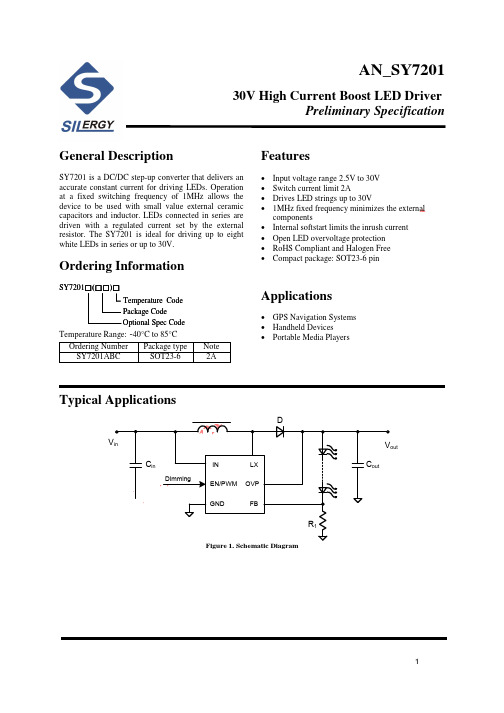
Features
• • • • • • • • Input voltage range 2.5V to 30V Switch current limit 2A Drives LED strings up to 30V 1MHz fixed frequency minimizes the external components Internal softstart limits the inrush current Open LED overvoltage protection RoHS Compliant and Halogen Free Compact package: SOT23-6 pin
Recommended Operating Conditions (Note 3) IN, ------------------------------------------------------------------------------------------------------------------- 2.5V to 30V LX, OVP ----------------------------------------------------------------------------------------------------------- 2.5V to 30V All other pins ------------------------------------------------------------------------------------------------------ 0 to 3.6V Junction Temperature Range ------------------------------------------------------------------------------------ -40°C to 125°C Ambient Temperature Range ----------------------------------------------------------------------------------- -40°C to HDN VREF IFB RDS(ON) ILIM VENH VENL VUVLO VHYS FOSC TSD THYST VOCL
IRFW720中文资料
(Note 4)(Note 4, 5)(Note 4, 5) (Note 4)Notes:1. Repetitive Rating : Pulse width limited by maximum junction temperature2. L = 39mH, I AS =3.3A, V DD = 50V, R G = 25 Ω, Starting T J = 25°C 3. I SD ≤ 3.3A, di/dt ≤ 300A/µs, V DD ≤ BV DSS, Starting T J = 25°C4. Pulse Test : Pulse width ≤300µs, Duty cycle ≤2%5. Essentially independent of operating temperatureI GSSRGate-Body Leakage Current, ReverseV GS = -30 V, V DS = 0 V-----100nAOn CharacteristicsV GS(th)Gate Threshold Voltage V DS = V GS , I D = 250 µA 2.0-- 4.0V R DS(on)Static Drain-Source On-ResistanceV GS = 10 V, I D = 1.65 A -- 1.4 1.75Ωg FSForward TransconductanceV DS = 40 V, I D = 1.65 A--2.8--SDynamic CharacteristicsC iss Input Capacitance V DS = 25 V, V GS = 0 V, f = 1.0 MHz--460600pF C oss Output Capacitance--5572pF C rssReverse Transfer Capacitance--1115pFSwitching Characteristicst d(on)Turn-On Delay Time V DD = 200 V, I D = 3.3 A,R G = 25 Ω--1030ns t r Turn-On Rise Time --3580ns t d(off)Turn-Off Delay Time --3580ns t f Turn-Off Fall Time --3580ns Q g Total Gate Charge V DS = 320 V, I D = 3.3 A,V GS = 10 V--1418nC Q gs Gate-Source Charge -- 2.7--nC Q gdGate-Drain Charge--5.6--nCDrain-Source Diode Characteristics and Maximum RatingsI S Maximum Continuous Drain-Source Diode Forward Current ---- 3.3A I SM Maximum Pulsed Drain-Source Diode Forward Current----13.2A V SD Drain-Source Diode Forward Voltage V GS = 0 V, I S = 3.3 A ---- 1.5V t rr Reverse Recovery Time V GS = 0 V, I S = 3.3 A,dI F / dt = 100 A/µs--220--ns Q rrReverse Recovery Charge-- 1.36--µCDISCLAIMERFAIRCHILD SEMICONDUCTOR RESERVES THE RIGHT TO MAKE CHANGES WITHOUT FURTHER NOTICE TO ANY PRODUCTS HEREIN TO IMPROVE RELIABILITY, FUNCTION OR DESIGN. FAIRCHILD DOES NOT ASSUME ANY LIABILITY ARISING OUT OF THE APPLICATION OR USE OF ANY PRODUCT OR CIRCUIT DESCRIBED HEREIN;NEITHER DOES IT CONVEY ANY LICENSE UNDER ITS PATENT RIGHTS, NOR THE RIGHTS OF OTHERS.LIFE SUPPORT POLICYFAIRCHILD’S PRODUCTS ARE NOT AUTHORIZED FOR USE AS CRITICAL COMPONENTS IN LIFE SUPPORT DEVICES OR SYSTEMS WITHOUT THE EXPRESS WRITTEN APPROVAL OF FAIRCHILD SEMICONDUCTOR CORPORATION.As used herein:1. Life support devices or systems are devices or systems which, (a) are intended for surgical implant into the body,or (b) support or sustain life, or (c) whose failure to perform when properly used in accordance with instructions for use provided in the labeling, can be reasonably expected to result in significant injury to the user.2. A critical component is any component of a life support device or system whose failure to perform can be reasonably expected to cause the failure of the life support device or system, or to affect its safety or effectiveness.PRODUCT STATUS DEFINITIONS Definition of TermsDatasheet Identification Product Status DefinitionAdvance InformationFormative or In Design This datasheet contains the design specifications for product development. Specifications may change in any manner without notice.PreliminaryFirst ProductionThis datasheet contains preliminary data, andsupplementary data will be published at a later date.Fairchild Semiconductor reserves the right to make changes at any time without notice in order to improve design.No Identification Needed Full ProductionThis datasheet contains final specifications. Fairchild Semiconductor reserves the right to make changes at any time without notice in order to improve design.Obsolete Not In ProductionThis datasheet contains specifications on a product that has been discontinued by Fairchild semiconductor.The datasheet is printed for reference information only.TRADEMARKSThe following are registered and unregistered trademarks Fairchild Semiconductor owns or is authorized to use and is not intended to be an exhaustive list of all such trademarks.STAR*POWER is used under licenseACEx™Bottomless™CoolFET™CROSSVOLT ™DenseTrench™DOME™EcoSPARK™E 2CMOS™EnSigna™FACT™FACT Quiet Series™FAST ®FASTr™FRFET™GlobalOptoisolator™GTO™HiSeC™ISOPLANAR™LittleFET™MicroFET™MicroPak™MICROWIRE™OPTOLOGIC™OPTOPLANAR™PACMAN™POP™Power247™PowerTrench ®QFET™QS™QT Optoelectronics™Quiet Series™SLIENT SWITCHER ®SMART START™STAR*POWER™Stealth™SuperSOT™-3SuperSOT™-6SuperSOT™-8SyncFET™TruTranslation™TinyLogic™UHC™UltraFET ®VCX™。
IRF7201TR中文资料
Top View
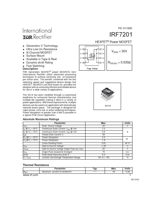
The SO-8 has been modified through a customized leadframe for enhanced thermal characteristics and multiple-die capability making it ideal in a variety of power applications. With these improvements, multiple devices can be used in an application with dramatically reduced board space. The package is designed for vapor phase, infra red, or wave soldering techniques. Power dissipation of greater than 0.8W is possible in a typical PCB mount application.
When mounted on 1 inch square copper board, t<10 sec
2
元器件交易网
ID , Drain-to-Source Current (A)
IRF7201
100
VGS
TOP
15V
10V
7.0V
5.5V
4.5V
0.1 0.4
VGS = 0V A
0.6
0.8
1.0
1.2
VSD , Source-to-Drain Voltage (V)
Fig 4. Typical Source-Drain Diode Forward Voltage
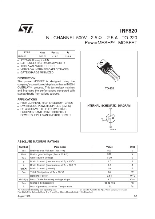
IRF820数据手册
mm TYP. MAX. 4.60 1.32 2.72 1.27 0.70 0.88 1.70 1.70 5.15 2.7 10.40 0.019 0.024 0.044 0.044 0.194 0.094 0.393 MIN. 0.173 0.048 0.094 4.40 1.23 2.40
inch TYP. MAX. 0.181 0.051 0.107 0.050 0.027 0.034 0.067 0.067 0.203 0.106 0.409 0.645 0.551 0.116 0.620 0.260 0.154 0.151
August 1998
1/8
IRF820
THERMAL DATA
R t hj-ca se
Rthj -amb
R thc- si nk Tl
Thermal Resistance Junction-case Max Thermal Resistance Junction-ambient Max Thermal Resistance Case-sink Typ Maximum Lead Temperature For Soldering Purpose
1.56 62.5 0.5 300
C/W oC/W o C/W o C
o
AVALANCHE CHARACTERISTICS
Symb ol I AR E AS Parameter Avalanche Current, Repetitive or Not-Repetitive (pulse width limited by Tj max) Single Pulse Avalanche Energy (starting Tj = 25 o C, I D = IAR , VDD = 50 V) Max Valu e 2.5 210 Unit A mJ
- 1、下载文档前请自行甄别文档内容的完整性,平台不提供额外的编辑、内容补充、找答案等附加服务。
- 2、"仅部分预览"的文档,不可在线预览部分如存在完整性等问题,可反馈申请退款(可完整预览的文档不适用该条件!)。
- 3、如文档侵犯您的权益,请联系客服反馈,我们会尽快为您处理(人工客服工作时间:9:00-18:30)。
ParameterMax.UnitsV DSDrain- Source Voltage30V I D @ T C = 25°C Continuous Drain Current, V GS @ 10V 7.3I D @ T C = 70°C Continuous Drain Current, V GS @ 10V 5.8A I DMPulsed Drain Current 58P D @T C = 25°C Power Dissipation 2.5P D @T C = 70°C Power Dissipation 1.6Linear Derating Factor 0.02W/°C V GS Gate-to-Source Voltage± 20V V GSM Gate-to-Source Voltage Single Pulse tp<10µs 30V E AS Single Pulse Avalanche Energy 70mJ dv/dt Peak Diode Recovery dv/dt5.0V/ns T J, T STGJunction and Storage Temperature Range-55 to + 150°CHEXFET ® Power MOSFETFifth Generation HEXFET ® power MOSFETs from International Rectifier utilize advanced processing techniques to achieve extremely low on-resistance per silicon area. This benefit, combined with the fast switching speed and ruggedized device design that HEXFET MOSFETs are well known for, provides the designer with an extremely efficient and reliable device for use in a wide variety of applications.The SO-8 has been modified through a customized leadframe for enhanced thermal characteristics and multiple-die capability making it ideal in a variety of power applications. With these improvements, multiple devices can be used in an application with dramatically reduced board space. The package is designed for vapor phase, infra red, or wave soldering techniques.Power dissipation of greater than 0.8W is possible in a typical PCB mount application.l Generation V Technology l Ultra Low On-Resistance l N-Channel MOSFET l Surface Mountl Available in Tape & Reel l Dynamic dv/dt Rating l Fast Switching lLead-FreeIRF7201PbFDescription9/30/04ParameterTyp.Max.UnitsR θJAMaximum Junction-to-Ambient–––50°C/WThermal ResistanceAbsolute Maximum RatingsW 1SO-8PD- 95022IRF7201PbFParameterMin.Typ.Max.Units Conditions V (BR)DSSDrain-to-Source Breakdown Voltage 30––––––V V GS = 0V, I D = 250µA∆V (BR)DSS /∆T JBreakdown Voltage Temp. Coefficient –––0.024–––V/°C Reference to 25°C, I D = 1mA ––––––0.030V GS = 10V, I D = 7.3A––––––0.050V GS = 4.5V, I D = 3.7A V GS(th)Gate Threshold Voltage 1.0––––––V V DS = V GS , I D = 250µA g fs Forward Transconductance 5.8––––––S V DS = 15V, ID = 2.3A –––––– 1.0V DS = 24V, V GS = 0V––––––25V DS = 24V, V GS = 0V, T J = 125°C Gate-to-Source Forward Leakage ––––––-100V GS = -20VGate-to-Source Reverse Leakage ––––––100V GS = 20V Q g Total Gate Charge–––1928I D = 4.6A Q gs Gate-to-Source Charge––– 2.3 3.5nC V DS = 24V Q gd Gate-to-Drain ("Miller") Charge ––– 6.39.5V GS = 10V, See Fig. 10 t d(on)Turn-On Delay Time –––7.0–––V DD = 15V t rRise Time–––35–––I D = 4.6At d(off)Turn-Off Delay Time –––21–––R G = 6.2Ωt f Fall Time–––19–––R D = 3.2Ω, C iss Input Capacitance –––550–––V GS = 0V C oss Output Capacitance–––260–––pF V DS = 25V C rssReverse Transfer Capacitance–––100–––ƒ = 1.0MHz, See Fig. 9Electrical Characteristics @ T J = 25°C (unless otherwise specified)I GSS µAΩR DS(on)Static Drain-to-Source On-Resistance I DSS Drain-to-Source Leakage Current nAnsSource-Drain Ratings and CharacteristicsRepetitive rating; pulse width limited bymax. junction temperature. (See fig. 11)I SD ≤ 4.6A, di/dt ≤ 120A/µs, V DD ≤ V (BR)DSS ,T J ≤ 150°CNotes:V DD = 15V, starting T J = 25°C, L = 6.6mHR G = 25Ω, I AS = 4.6A. (See Figure 8)Pulse width ≤ 300µs; duty cycle ≤ 2%.When mounted on 1 inch square copper board, t<10 secIRF7201PbF 3Fig 3. Typical Transfer CharacteristicsFig 2. Typical Output CharacteristicsFig 1. Typical Output Characteristics 1101000.1110DSV , Drain-to-Source Voltage (V)D I , D r a i n -t o -S o u r c e C u r r e n t (A )1101000.1110DSV , Drain-to-Source Voltage (V)D I , D r a i n -t o -S o u r c e C u r r e n t (A )1101003.03.54.04.55.05.5GSV , Gate-to-Source Voltage (V)D I , D r a i n -t o -S o u r c e C u r r e nt (A )Fig 4. Typical Source-Drain DiodeForward Voltage0.11101000.40.60.81.01.2V , Source-to-Drain Voltage (V)I , R e v e r s e D r a i n C u r r e n t (A )SDS DIRF7201PbFFig 5. Normalized On-ResistanceVs. Temperature0.00.51.01.52.0-60-40-2020406080100120140160JT , Junction Temperature (°C)R , D r a i n -t o -S o u r c e O n R e s i s t a n c e D S (o n)(N o r m a l i z e d )Fig 8. Maximum Avalanche EnergyVs. Drain Current04080120160200255075100125150JE , S i n g l e P u l s e A v a l a n c h e E n e r g y (m J )A SStarting T , Junction Temperature (°C)Fig 6. On-Resistance Vs. Drain CurrentFig 7. On-Resistance Vs. Gate Voltage0.020.030.040.05246810121416R , D r a i n -t o -S o u r c e O n R e s i s t a n c e D S (o n)(Ω)GSV , Gate-to-Source Voltage (V)0.000.050.100.150.2010203040I , Drain Current (A)D(Ω)D S (o n)R , D r a i n -t o -S o u r c e O n R e s i s t a n c eIRF7201PbF 5Fig 10. Typical Gate Charge Vs.Gate-to-Source VoltageFig 9. Typical Capacitance Vs.Drain-to-Source Voltage Fig 11. Maximum Effective Transient Thermal Impedance, Junction-to-Ambient02004006008001000110100C , C a p a c i t a n c e (p F )DS V , Drain-to-Source Voltage (V)04812162051015202530Q , Total Gate Charge (nC)GV , G a t e -t o -S o u r c e V o l ta g e (V )G SIRF7201PbFSO-8 Package OutlineIRF7201PbF 7330.00(12.992) MAX.14.40 ( .566 )12.40 ( .488 )NOTES :1. CONTROLLING DIMENSION : MILLIMETER.2. OUTLINE CONFORMS TO EIA-481 & EIA-541.FEED DIRECTIONTERMINAL NUMBER 112.3 ( .484 )11.7 ( .461 )8.1 ( .318 )7.9 ( .312 )NOTES:1. CONTROLLING DIMENSION : MILLIMETER.2. ALL DIMENSIONS ARE SHOWN IN MILLIMETERS(INCHES).3. OUTLINE CONFORMS TO EIA-481 & EIA-541.SO-8 Tape and ReelDimensions are shown in milimeters (inches)Data and specifications subject to change without notice.This product has been designed and qualified for the Consumer market.Qualifications Standards can be found on IR’s Web site.IR WORLD HEADQUARTERS: 233 Kansas St., El Segundo, California 90245, USA Tel: (310) 252-7105TAC Fax: (310) 252-7903Visit us at for sales contact information .09/04分销商库存信息:IRIRF7201TRPBF IRF7201PBF。