TM162AAA6-1中文资料
INA-30311资料

DescriptionHewlett-Packard’s INA-30311 is a Silicon monolithic amplifier for applications to 1.0 GHz. Packaged in a miniature SOT-143 package,it requires very little board space.The INA-30311 uses an internally biased topology which eliminates the need for external components and provides decreased sensitiv-ity to ground inductance.The INA-30311 is designed with an output impedance that varies from near 200 Ω at lowfrequencies to near 50 Ω at higher frequencies. This provides a matching advantage for IF circuits, as well as improved power efficiency, making it suitable for battery powered designs.The INA-30311 is fabricated using HP’s 30 GHz f MAX ISOSAT TM Silicon bipolar process which uses nitride self-alignment sub-micrometer lithography, trench isolation, ion implantation, gold metallization, and polyimide intermetal dielectric and scratch protection to achieve superior performance, uniformity, and reliability.1 GHz Low Noise Silicon MMIC Amplifier Technical DataINA-30311Features• Internally Biased, Single 3 V Supply (6 mA)• 3.5 dB NF • 13 dB Gain• Unconditionally StableApplications• LNA or IF Amplifier for Cellular, Cordless, Special Mobile Radio, PCS, ISM, and Wireless LAN ApplicationsSOT-143 Surface MountPackagePin Connections and Package MarkingEquivalent Circuit (Simplified)GNDOUTPUTINPUTV CCAbsolute Maximum RatingsAbsolute Symbol ParameterUnits Maximum [1]V CC Device Voltage, to ground V 12P in CW RF Input Power dBm +13T j Junction Temperature °C 150T STGStorage Temperature°C-65 to 150INA-30311 Electrical Specifications [3], T C = 25°C, Z O = 50 Ω, V CC = 3 VSymbol Parameters and Test ConditionsUnits Min.Typ.Max.G p Power Gain (|S 21|2) f = 900 MHz dB 1113NF Noise Figuref = 900 MHz dB 3.5P 1dB Output Power at 1 dB Gain Compression f = 900 MHz dBm -11IP 3Third Order Intercept Point f = 900 MHz dBm-2VSWR Input VSWR f = 900 MHz1.7I cc Device Current mA 6.37.5ιdGroup Delayf = 900 MHz ps 325INA-30311 Typical Scattering Parameters [3], T C = 25°C, Z O = 50 Ω, V CC = 3 VFreq.S 11S 21S 12S 22K GHz Mag Ang dB Mag Ang dB Mag Ang Mag Ang Factor 0.050.09-116.12 6.40-6-38.10.01220.57-1 4.350.100.09-216.11 6.39-12-38.20.01240.56-3 4.430.200.10-616.12 6.40-25-38.40.01280.56-7 4.410.300.13-1616.14 6.41-38-38.90.011130.55-11 4.830.400.16-2916.07 6.36-52-39.40.011190.54-14 4.880.500.18-4215.90 6.24-66-40.10.010270.52-18 5.600.600.21-5915.56 6.00-81-40.70.009400.50-20 6.580.700.22-7515.04 5.65-95-40.70.009570.47-237.260.800.24-9214.34 5.21-109-39.60.011740.46-24 6.490.900.25-10713.44 4.70-122-37.60.013860.44-24 6.231.000.26-12212.53 4.23-135-35.50.017940.43-25 5.351.200.27-14410.50 3.35-155-32.30.0241000.42-26 4.831.400.27-1628.50 2.66-173-29.60.0331010.42-27 4.431.600.27-177 6.69 2.16172-27.50.0421000.42-28 4.311.800.27173 5.01 1.78159-25.70.052990.42-30 4.222.000.27163 3.58 1.51147-24.10.062970.42-32 4.172.200.27156 2.35 1.31136-22.50.075950.42-35 3.972.400.26150 1.21 1.15126-21.40.085920.41-37 4.042.500.261470.751.09122-20.90.091910.41-393.99Note:3. Reference plane per Figure 9 in Applications Information section.Thermal Resistance [2]:θj-c = 550°C/WNotes:1. Operation of this device above any one of these limits may cause permanent damage.2. T C = 25°C (T C is defined to be thetemperature at the package pins where contact is made to the circuit board).INA-30311 Typical Performance, T C = 25°C, Z O = 50 Ω, V CC = 3 VFigure 7. Input and Output VSWR vs.Frequency.Figure 8. Supply Current vs. Voltage and Temperature.Figure 1. Power Gain vs. Frequency and Voltage.Figure 2. Noise Figure vs. Frequency and Voltage.G A I N (d B )0.10FREQUENCY (GHz)0.7201051.515 1.10.30.50.9 1.3 3.3 V 3.0 V 2.7 VN O I S E F I G U R E (d B )0.10FREQUENCY (GHz)0.74.02.01.0 1.53.0 1.10.30.50.9 1.3 2.7 V 3.0 V 3.3 V0.51.52.53.5P 1 d B (d B m )0.1-14FREQUENCY (GHz)0.70-6-10 1.5-4 1.10.30.50.9 1.33.3 V 3.0 V2.7 V -12-8-2V S W R (n :1)FREQUENCY (GHz)Figure 5. Noise Figure vs. Frequency and Temperature.Figure 6. Output Power for 1 dB Gain Compression vs. Frequency and Temperature.G A I N (d B )0.10FREQUENCY (GHz)0.7201051.515 1.10.30.50.9 1.3-40+25+85N O I S E F I G U R E (d B )0.10FREQUENCY (GHz)0.7521 1.541.10.30.50.9 1.3-40+25+853P 1 d B (d B m )0.1-12FREQUENCY (GHz)0.7-8-10-111.5-91.10.30.50.9 1.3-40+25+85Figure 3. Output Power for 1 dB Gain Compression vs. Frequency and Voltage.Figure 4. Gain vs. Frequency and Temperature.I C C (mA )V CC (V)INA-30311 Applications InformationIntroductionThe INA-30311 is a silicon RF integrated circuit that provides an easy-to-use solution for low noise or multi-purpose gain block applications up to 1000 MHz. This two-stage amplifier design uses resistive feedback to provide flat gain over a wide frequency range. This device is assembled in a miniature, surface mount package and is intended for use in low cost wireless communication products.A unique feature of the INA-30311 is that it is designed with a 50Ωinput impedance and an output impedance that approaches 200Ωat lower frequencies. This imped-ance converting feature is very useful for applications such as receiver IF circuits in which the INA-30311 is followed by highinput impedance devices like signal processing circuits, filters, or mixed signal ICs.In addition to simplifying the match to higher impedance devices, a key benefit of the higher output impedance feature is an improvement in power efficiency.Phase Reference PlanesThe positions of the reference planes used to measureS-Parameters are shown in Figure9. As seen in the illustra-tion, the reference planes are located at the point where the package leads contact the test circuit.MATCHEDΩOUTPUT BiasingThe INA-30311 is a voltage biaseddevice and operates from a single+3 volt power supply. With acurrent drain of 6 mA, thisamplifier is suitable for use inbattery powered applications. Allbias circuitry is fully integratedinto the IC eliminating the needfor external DC components. RFperformance is very stable for3-volt battery supplies that mayrange from 2.7 to 3.3 volts,depending on battery “freshness”or state of charge in the case ofrechargeable batteries.While the INA-30311 wasdesigned for use in +3 volt batterypowered applications, theinternal bias regulation circuitryallows it to be used with anypower supply voltage from +2.7to +5 volts.Typical ConfigurationsThe way in which the INA-30311is used depends on the particularapplication and operatingfrequency.• For receiver IF amplifier appli-cations up to several hundredMHz, the relatively higher out-put impedance level of theINA-30311 may be used toadvantage when interfacingdirectly with devices havinghigher than 50Ω input imped-ances, such as certain signalprocessing or mixed signal ICs.This application is shown inFigure 10.• A second implementation,shown in Figure 11, uses asimple reactive network at theamplifier’s output to match theoutput impedance to 50 Ω.This matched output arrangementwill provide an additional 0.9 dBof gain and output power at900MHz when driving into a 50Ωstage.• The third way to use the INA-30311 is to simply cascadeseveral INA-30311’s with 50Ωstages and neglect the effects ofthe output mismatch.The 50 Ω cascade withoutimpedance matching, shown inFigure 12, trades off theimprovement in stage gain andoutput power for a moresimplified interstage circuit andreduced circuit board space.Figure 11. Impedance MatchedOutput.Figure 12. Simple Cascade withoutImpedance Matching.Figure 10. INA-30311 Driving a HighInput Impedance Stage.RF RFFigure 13. Basic Amplifier Application.900 MHz Matched ExampleThis section describes ademonstration circuit for900␣MHz that is based on thematched output configurationshown in Figure11.The output VSWR of the INA-30311 is approximately 2.6:1 at900 MHz and results in a 0.9 dBmismatch loss when used in a50Ω system. The use of a simpleimpedance matching circuit at theoutput will increase both gain andoutput power by 0.9 dB. Thenoise figure of the amplifierremains the same and does notdepend on whether or not theoutput is matched.There are many circuit topologiesthat may be used to match theoutput impedance of theINA-30311 to a 50 Ω load. Theexample presented in Figure 15 isdesigned to match the amplifier’soutput for frequencies near900␣MHz.This circuit is representative forapplications in the 800 MHzcellular or 900 MHz unregulatedfrequency bands. This exampleuses a series capacitor to resonatewith a shunt, high impedancetransmission line. The transmis-sion line is tapped at a 50 Ω levelfor the output. This circuitprovides the desired impedancetransformation with a minimumof components, using only onechip capacitor that also doublesas the output DC block.used to the amplifier to the V CCsupply, additional bypasscapacitors may be needed toprevent resonances that wouldotherwise result in undesirablegain responses. A well-bypassedV CC line is also desirable toprevent possible oscillations thatmay occur due to feedbackthrough the bias line from otherstages in a cascade.Adequate grounding is needed toobtain maximum performance.The ground pin of the INA-30311should be connected to directlyto RF ground by using platedthrough holes (vias) near thepackage terminals.FR-4 or G-10 PCB material is agood choice for most low costwireless applications. Typicalboard thickness is 0.025 or0.031␣inches. The width of 50 Ωmicrostriplines in these PCBthicknesses is also convenient formounting chip components suchas the series DC blockingcapacitors.50 Ω ExampleThe demonstration circuit in Figure14 shows the INA-30311 usedwithout output impedancematching and is an example of thecascade depicted in Figure 12. Thislayout illustrates the simplestimplementation of the INA-30311by using 50 Ω microstriplineswith DC blocking capacitors forboth the input and output. TheV CC supply connection is RFbypassed very close to the lead ofthe RFIC. Provision is also madefor an additional bypass capacitoron the V CC line near the edge ofthe PCB.Operating DetailsThe basic application of the INA-30311 is shown in Figure 13. DC blocking capacitors should be placed in series with the RF Input and RF Output to isolate adjoin-ing circuits from the internal bias voltages that are present at these terminals. The values of the blocking capacitors are deter-mined by the lowest frequency of operation for a particular applica-tion. The capacitor’s reactances are chosen to be 5% or less of the amplifier’s input or output imped-ance at the lowest operating frequency. For example, an ampli-fier to be used in an application covering the 902 to 928 MHz band would require an input blocking capacitor of at least 70pF, which is 2.5 Ω of reactance, or 5% of50␣Ω at 902MHz.The V CC connection to the amplifier must be RF bypassed by placing a capacitor to ground directly at the bias pin of the package. Like the DC blocking capacitors, the value of the V CC bypass capacitor is determined by the lowest operating frequency for the ampli-fier. This value is typically the same as that of the DC blocking capacitors. If long bias lines areINA-30311 Part Number Ordering InformationPart Number Devices per ContainerContainer INA-30311-TR13,0007" reel INA-30311-BLK100Antistatic bagFigure 14. 50 Ω Input/Output Example.Figure 15. Matched Output Example.DIMENSIONS ARE IN MILLIMETERS (INCHES)0.10 (0.004) 0.013 (0.0005)END VIEWSIDE VIEWPackage Dimensions。
设备介绍-1662SMC

未经本公司书面授权,任何人不得擅自传播、复制、交流与使用本文档的部分或全部内容。
未经本公司书面授权,任何人不得擅自传播、复制、交流与使用本文档的部分或全部内容。
未经本公司书面授权,任何人不得擅自传播、复制、交流与使用本文档的部分或全部内容。
未经本公司书面授权,任何人不得擅自传播、复制、交流与使用本文档的部分或全部内容。
未经本公司书面授权,任何人不得擅自传播、复制、交流与使用本文档的部分或全部内容。
未经本公司书面授权,任何人不得擅自传播、复制、交流与使用本文档的部分或全部内容。
未经本公司书面授权,任何人不得擅自传播、复制、交流与使用本文档的部分或全部内容。
设备/系统应用组网方式1662SMC 能够在G.652、G.653、G.654等光纤上传输,其主要应用领域包括: 本地和城域环;城域网的多业务数据中心;带中间分插或再生站点的点到点链路; 集成光放大器的超长途传输。
未经本公司书面授权,任何人不得擅自传播、复制、交流与使用本文档的部分或全部内容。
线形结构未经本公司书面授权,任何人不得擅自传播、复制、交流与使用本文档的部分或全部内容。
未经本公司书面授权,任何人不得擅自传播、复制、交流与使用本文档的部分或全部内容。
Edited by Foxit ReaderCopyright(C) by Foxit Software Company,2005-2007未经本公司书面授权,任何人不得擅自 传播、复制、交流与使用本文档的部分或全部内容。
未经本公司书面授权,任何人不得擅自 传播、复制、交流与使用本文档的部分或全部内容。
未经本公司书面授权,任何人不得擅自 传播、复制、交流与使用本文档的部分或全部内容。
顺东SD563A说明书
【品名】顺东SD-563A码表/自行车码表【型号】SD-563A;【材质】工程塑料,LCD显示屏,电子元件等;【尺寸】表头尺寸57*40*17MM,显示屏尺寸:34*31MM;【电源】表头:1节3V CR2032锂电池(含)【包装】PVC吊卡;【附件】中文说明书【功能说明】1.SPD CURRENT SPEED/行车速度;2.ODO ODOMETER/行车总里程(0-9999KM);3.DST TRIP DISTANCE/单次行车里程;4.MAX MAXIMUN SPEED/最大行车速度;5.A VS A VERAGE SPEED/平均速度;6.OTM TOTOL TRIP TIME /累计行车时间;7.TM TRIP TIME/单次行车时间;8.RTM RIDING TRIP TIME/单次行程时间;9.CLK CLOCK/(12H/24H)时钟;10.SW STOP W A TCH/秒表;11.TEMPERTERA TURE /测量环境温度(-10℃~50℃)12.TM UP TRIP TIME UP /行车时间正计;13..TM DN TRIP TIME DOWN /行车时间倒计;14.TRIP UP TRIP DISTANCE UP/行车里程正计;15.TRIP DN TRIP DISTANCE DOWN/行车时间倒计;16..“+”“-”COMPARA TOR/速度对比提示;17.MAINTENANCE ALERT /保养提醒功能;18.LOW-SPEED REMINDER /加油提醒;19.OVER-SPEED REMINDER /超速提醒;20.SEETING TYRE CIRCUMFERENCE/胎圆周设定(0mm-9999mm);21.SEETING THE LAST V ALUE OF ODOMETER/总里程初始值设定(公里/英里);22.SETTING OTM /累计时间初始设定23.FREEZE FRAME MEMORY /行车资料采样功能;24.AUTO ON/OFF / 开/关;设置功能1、将电池装及表头背面的电池槽;2、在15秒内按右键进入车胎圆周长设置;3、参阅轮径与周长对照表,比如28车型轮周长为224cm,按左键将三位数值设定为224(本机预设为208cm4、右键确定;5、怎么还出来一串东西?先不用管它,直接右键确定,试车去吧。
TK2019资料

THERMAL CHARACTERISTICS
TC2001
SYMBOL θJA
PARAMETER JunctFra bibliotekon-to-ambient Thermal Resistance (still air)
Value 80
UNITS °C/W
2
TK2019 – MC/2.1/10-03
元器件交易网
ELECTRICAL CHARACTERISTICS – TK2019
TA = 25 °C. See Application/Test Circuit. Unless otherwise noted, the supply voltage is VDD = 24V.
SYMBOL Iq IMUTE VIH VIL ISC IVPPSENSE PARAMETER Quiescent Current (No load, Mute = 0V) Mute Supply Current (No load, TC2001 Mute = 5V, TPS1035 Sleep = 5V) High-level input voltage (MUTE) Low-level input voltage (MUTE) Short circuit current limit VPPSENSE Threshold Currents CONDITIONS VDD = 24V V5 = 5V VDD = 24V V5 = 5V IIH = See Mute Control Section IIL = See Mute Control Section VDD = 24V, T=25oC Over-voltage turn on (muted) Over-voltage turn off (mute off) Under-voltage turn off (mute off) Under-voltage turn on (muted) Over-voltage turn on (muted) Over-voltage turn off (mute off) Under-voltage turn off (mute off) Under-voltage turn on (muted) 7.5 162 154 79 72 30.3 28.8 14.8 13.5 3.5 1.0 178 87 33.3 16.3 MIN. TYP. 20 27 2 7 MAX. 60 UNITS mA mA µA mA V V A µA µA µA µA V V V V
MX620B芯片手册中文版

概述该产品为电池供电的玩具、低压或者电池供电的运动控制应用提供了一种集成的有刷直流马达驱动解决方案。
电路内部集成了采用N沟和P沟功率MOSFET设计的H桥驱动电路,适合于驱动有刷直流马达或者驱动步进马达的一个绕组。
该电路具备较宽的工作电压范围(从2V到9.6V),最大持续输出电流达到2A,最大峰值输出电流达到 3.5A。
该驱动电路内置过热保护电路。
通过驱动电路的负载电流远大于电路的最大持续电流时,受封装散热能力限制,电路内部芯片的结温将会迅速升高,一旦超过设定值(典型值150℃),内部电路将立即关断输出功率管,切断负载电流,避免温度持续升高造成塑料封装冒烟、起火等安全隐患。
内置的温度迟滞电路,确保电路恢复到安全温度后,才允许重新对电路进行控制。
该驱动电路内置限流保护电路。
当流过功率管的电流超过设定值时,内部电路限流保护电路启动,功率管最大输出电流将被限制在设定值。
该功能可确保电路输出端口与地短路、输出端口之间短路时,电路不烧毁。
特性●低待机电流(小于0.1uA);●低静态工作电流;●集成的H桥驱动电路;●内置防共态导通电路;●低导通内阻的功率MOSFET管;●内置带迟滞效应的过热保护电路(TSD);●内置限流保护电路,输出对地短路,输出与输出短路,不烧电路;●抗静电等级:3KV(HBM)。
典型应用●2-6节AA/AAA干电池供电的玩具马达驱动;●2-6节镍-氢/镍-镉充电电池供电的玩具马达驱动;●1-2节锂电池供电的马达驱动订购信息应用说明1、基本工作模式a)待机模式在待机模式下,INA=INB=L。
包括驱动功率管在内的所有内部电路都处于关断状态。
电路消耗极低极低的电流。
此时马达输出端OUTA和OUTB 都为高阻状态。
b)正转模式正转模式的定义为:INA=H,INB=L,此时马达驱动端OUTA输出高电平,马达驱动端OUTB输出低电平时,马达驱动电流从OUTA流入马达,从OUTB流到地端,此时马达的转动定义为正转模式。
911KD10JX中文资料

182KD10JX*thru180LD10JX*11 to 1000 VoltsVaristor2.6 to 247JouleFeatures• High Surge, High Energy• Designed to be Operated Continuously Across AC Power Lines • No Derating Up to 85к Ambient• Available in Tape and Reel or Bulk PackMaximum Ratings• Operating Ambient Temperature Range: -55к to +85к• Storage Temperature Range: -55к to +125к• Temperature Coefficient (өV) of Clamping Voltage (V C ) at Specified Test Current:<0.05%/к•Varistor voltage temperature coefficient:CURRENT, ENERGY AND POWER DERATING CURVE-551606080100120204060AMBIENT TEMPERATURE (°C)PERCENT OF RATED VALUE14080100120•UL Recognized File # E306895(UL1449) and E306942(UL1414)omp onents 20736 Marilla Street Chatsworth! "# $ % ! "#TMMicro Commercial ComponentsNote : 'X' can be S, C, I or Y .*'S' denotes straight lead'C' denotes out crimped lead 'I' denotes inner crimped lead 'Y' denotes kink lead160x(100/ć)182KD10JX thru 180LD10JX*680K-180L Max. Clamping Voltage testing current 5A .(V)(V)(J)(V)(V)182KD10JX 10001465247.01800(1620-1980)2970112KD10JX 680895155.01100(990-1210)1815102KD10JX 625825140.01000(900-1100)1650911KD10JX 550745127.0910(819-1001)1500821KD10JX 510670118.0820(738-902)1355781KD10JX 485640116.0780(702-858)1290751KD10JX 460615115.0750(675-825)1240681KD10JX 420560112.0680(612-748)1120621KD10JX 385505107.0620(558-682)1025561KD10JX 350460102.0560(504-616)920511KD10JX 32041892.0510(459-561)845471KD10JX 30038585.0470(423-517)775431KD10JX 27535080.0430(387-473)710391KD10JX 25032070.0390(351-429)650361KD10JX 23030065.0360(324-396)595331KD10JX 21027558.0330(297-363)550301KD10JX 19525052.0300(270-330)505271KD10JX 17522549.0270(243-297)455241KD10JX 15020042.0240(216-264)395221KD10JX 14018039.0220(198-242)360201KD10JX 13017035.0200(180-220)330181KD10JX 11515032.0180(162-198)300151KD10JX 9512525.0150(135-165)250121KD10JX 7510022.0120(108-132)200101KD10JX 608518.0100(90-110)165820KD10JX 506514.082(74-90)135680KD10JX 40569.868(61-75)*135560KD10JX 35458.156(50-62)*110470KD10JX 3038 6.847(42-52)*93390KD10JX 2531 5.639(35-43)*77330KD10JX 2026 4.833(30-36)*65270KD10JX 1722 3.927(24-30)*53220KD10JX 1418 3.222(20-24)*43180LD10J X11142.618(15-21)*36V25A (A)10005000.05350025000.4Rated WattageVaristor VoltageMaximum Clamping Voltage ACrms DC 10/1000us1 time2 times(W)V1mA Part NumberMaximum AllowableVoltageMaximum EnergyWithstanding Surge Current 8/20usElectrical Characteristics @ 25O C Unless Otherwise NotedMicro Commercial Components570504030AV-I Curve (820K to 561K)V100908060200907069580605020400300200150100AV-I Curve (180L to 680K)VTMMicro Commercial Components2000400030005000AV-I Curve (621K to 182K)V1100101000100V-I Surge Life Time Ratings (180L to 680K)AµsImpulse Current – AmperesImpulse Width – Micro seconds101001001000V-I Surge Life Time Ratings (820K to182K)AµsImpulse Current – Amperes Impulse Width – Micro secondsMicro Commercial ComponentsNote 2.T Thickness (max.)Unit:mmMicro Commercial ComponentsPart CodeD05D07D10D14D20182K 12.612.813.5112K 10.510.711.2102K 9.910.110.7911K 9.49.610.1821K 8.38.89.09.5781K 8.18.68.89.3751K 7.97.98.48.69.1681K 7.57.58.08.28.7621K 7.27.27.67.88.3561K 6.9 6.97.37.58.0511K 6.6 6.67.07.27.7471K 6.4 6.4 6.87.07.5431K 6.1 6.1 6.5 6.77.2391K 5.3 5.3 5.7 5.9 6.4361K 5.1 5.1 5.5 5.7 6.2331K 4.9 4.9 5.3 5.5 6.0301K 4.8 4.8 5.2 5.4 5.9271K 4.6 4.6 5.0 5.2 5.7241K 4.4 4.4 4.8 5.0 5.5221K 4.3 4.3 4.7 4.9 5.4201K 4.2 4.2 4.6 4.8 5.3181K 4.1 4.1 4.5 4.7 5.2151K 4.5 4.5 4.9 5.1 5.6121K 4.1 4.1 4.5 4.6 5.3101K 3.9 3.9 4.4 4.5 5.1820K 3.8 3.8 4.3 4.4 4.9680K 5.5 5.5 6.0 6.1 6.1560K 5.0 5.0 5.5 5.6 5.6470K 5.0 5.0 5.5 5.6 5.6390K 4.7 4.7 5.1 5.2 5.4330K 4.7 4.7 5.1 5.2 5.4270K 4.7 4.7 5.1 5.2 5.4220K 4.5 4.5 4.9 5.0 5.3180L4.54.54.95.05.2Micro Commercial Components***IMPORTANT NOTICE***Micro Commercial Components Corp.reserve s the right to make changes without further notice to any product herein to make corrections, modifications , enhancements , improvements , or other changes .Micro Commercial Components Corp.does not assume any liability arising out of the application or use of any product described herein; neither does it convey any license under its patent rights ,northe rights of others . The user of products in such applications shall assume all risks of such use and will agree to hold Micro Commercial Components Corp.and all the companies whoseproducts are represented on our website, harmless against all damages.***APPLICATIONS DISCLAIMER***Products offer by Micro Commercial Components Corp.are not intended for use in Medical,Aerospace or Military Applications.。
TVR07471中文资料
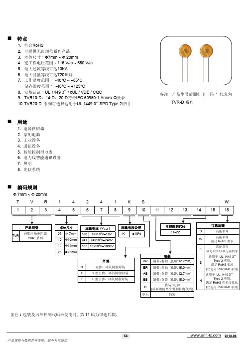
产品类型 TVR 兴勤压敏电阻器 TVR 系列
本体尺寸 07 10 14 20 Φ 7mm Φ10mm Φ14mm Φ20mm
压敏电压 (V1mA ) 180 241 18x10 V=18V 24x10 V=240V
2 1 0
压敏电压公差 K ±10%
内部控制代码 01~ZZ D W K 包装
可选后辍
S
N
备注:包装及内部控制代码未使用时, 第 11 码为可选后辍。
54
2013.03
产品规格与数据若有变更,恕不另行通知
压敏电阻交易www.unit-ic.com
结构与尺寸
S 型 (直脚)
D T
A
Max. 3.0
P W
仰视图
P
d
L
W
(单位:mm) 系列 TVR07-D TVR10-D TVR14-D TVR20-D D 7.5~9.5 12.0~14.0 16.0~18.5 22~24.5 Lmin. 26.5 26.5 26.5 22.5 d 0.6±0.02 0.8±0.02 0.8±0.02 1.0±0.02 P 5±1 7.5±1 7.5±1 10±1 Amax. 12.5 17.5 21.5 28.5
请见电气特性表
Tmax.
W
F 型 (Y型引脚)
D T
Max.3.0
A
MAX 30
0
P
C d
(单位:mm) 系列 TVR07-D TVR10-D TVR14-D TVR20-D D 7.5~9.5 12.0~14.0 16.0~18.5 22~24.5 Cmin. 20 20 20 20 d 0.6±0.02 0.8±0.02 0.8±0.02 1.0±0.02 P 5±1 7.5±1 7.5±1 10±1 Amax. 12.5 18.0 22.0 29.0
(参考资料)SJ-D主轴参数

12 0 0 0 0 0 0 0 0 0 0 0 2
22 120
0 10000
1500 1800 1262
73 3252 2427 1947
145 0 0 0
Name SP145 SP146 SP147 SP148 SP149 SP150 SP151 SP152 SP153 SP154 SP155 SP156 SP157 SP158 SP159 SP160 SP161 SP162 SP163 SP164 SP165 SP166 SP167 SP168 SP169 SP170 SP171 SP172 SP173 SP174 SP175 SP176 SP177 SP178 SP179 SP180 SP181 SP182 SP183 SP184 SP185 SP186 SP187 SP188 SP189 SP190 SP191 SP192
Set1 15 33 15 0 150
1900 0
150 1900
0 0 0 0 50 100 20 000C 0000 2000 2000 60 120 120 875 875 10000 25 1000 30 0 2200 0019 0000 0000 1600 0000 100 0 0 0 0 0 0 0 0 0 100 0
[Set1] Drive unit
:MDS-D-SP-160
[Set2] Drive unit
:MDS-D-SPJ3-75
Power supply unit:MDS-D-CV-□
Power supply unit:FCUA-RB□/R-UNIT□
Motor
:SJ-D7.5/100-01+MBE205(2000kp/rev)
- 1、下载文档前请自行甄别文档内容的完整性,平台不提供额外的编辑、内容补充、找答案等附加服务。
- 2、"仅部分预览"的文档,不可在线预览部分如存在完整性等问题,可反馈申请退款(可完整预览的文档不适用该条件!)。
- 3、如文档侵犯您的权益,请联系客服反馈,我们会尽快为您处理(人工客服工作时间:9:00-18:30)。
! "#$ % #1.1 Display type: TN1.2 Display color*:Display color: Blue-BlackBackground: White1.3 Polarizer mode: Reflective/Positive1.4 Viewing Angle: 6:001.5 Driving Method: 1/16 Duty 1/5 Bias1.6 Backlight: None1.7 Display Fonts: 5 x 7 dots + Cursor (1 Character)1.8 Controller: HCD66701A001.9 Data Transfer: 8 Bit Parallel1.10 Operating Temperature: 0----+50Storage Temperature: -20----+601.11 Outline Dimensions: Refer to outline drawing on next page1.12 Dot Matrix: 16 Characters X 2 Lines1.13 Dot Size: 0.55X0.50(mm)1.14 Dot Pitch: 0.60X0.55 (mm)1.15 Weight: 20g1.16 PCB edtion: TM162AD P1-2* Color tone is slightly changed by temperature and driving voltage.2. Outline Drawing) * + '# '! !NONE 6!, ' -# !. #' + / !'!Item Symbol Min. Max. Unit RemarkPower Supply Voltage V V -0.3 7.0LCD Driving Voltage V -0.3 13.0 VOperating Temperature RangeT0 +50Storage TemperatureRangeT-20 +60NoCondensation0 # # '6.1 Electrical characteristicsItem SymbolMin.Typ.Max.Unit Supply Voltage(Logic)V V 4.5 5.0 5.5 VSupply Voltage(LCD Drive)V - 4.7 - VHighVV=5.00.7V - V +0.3 VInput SignalVoltageLowVV=5.0-0.3 - 0.2 VVSupply current (Logic)IV V =5.0- 1.5 2.0mASupply current(LCD Drive) I - 0.40 0.6mA6.2 Interface SignalsPin No. Symbol Level DescriptionGround1 Vss 0V2 Vcc 5.0V Power supply voltage for logic and LCD(+)3 Vee 0.3V Power supply voltage for LCD(-)4 RS H/LregistersSelects5 R/W H/L Selects read or write6 E H/L Starts data read/writebit07 DB0 H/LDatabit1Data8 DB1 H/Lbit2Data9 DB2 H/Lbit3Data10 DB3 H/Lbit4Data11 DB4 H/Lbit5Data12 DB5 H/Lbit6Data13 DB6 H/Lbit7Data14 DB7 H/L" NC -signalNoNC -signalNo6.3 Interface Timing ChartAC Characteristics (VCC= 2.7 to 5.5V, Ta= –30 to +75°C*3)Write OperationItem Symbol Min Typ Max Unit Test ConditionEnable cycle time tcycE1000 — — nsEnable pulse width (high level)PWEH450——Enable rise/fall time tEr, tEf——25Address set-up time (RS, R/W to E)tAS40——Address hold time tAH20——Data set-up time tDSW195——Data hold time tH10——Read OperationItem Symbol Min Typ Max Unit Test ConditionEnable cycle time tcycE1000 — — nsEnable pulse width (high level)PWEH450——Enable rise/fall time tEr, tEf——25Address set-up time (RS, R/W to E)tAS40——Address hold time tAH20——Data delay time tDDR——350Data hold time tDHR10——Timing Characteristics Write OperationRead Operation6.4 Instruction CodeCodeExecution Time(max) (when fcporInstruction RS R/W DB7DB6DB5DB4DB3DB2DB1DB0Description fOSCis 320 kHz) Cleardisplay0000000001Clears entire display andsets DDRAM address 0 inaddress counter.1.28 msReturnhome000000001—Sets DDRAM address 0 inaddress counter. Alsoreturns display from beingshifted to original position.DDRAM contents remainunchanged.1.28 msEntry modeset00000001I/D S Sets cursor move directionand specifies display shift.These operations areperformed during data writeand read.31 µsDisplayon/offcontrol0000001D C B Sets entire display (D)on/off, cursor on/off (C), andblinking of cursor positioncharacter (B).31 µsCursor ordisplay shift000001S/C R/L——Moves cursor and shiftsdisplay without changingDDRAM contents.31 µsFunctionset00001DL N F——Sets interface data length(DL), number of displaylines (L), and character font(F).31 µsSetCGRAMaddress0001ACG ACG ACG ACG ACG ACG Sets CGRAM address.CGRAM data is sent andreceived after this setting.31 µsSetDDRAMaddress001ADD ADD ADD ADD ADD ADD ADD Sets DDRAM address.DDRAM data is sent andreceived after this setting.31 µsRead busyflag &address01BF AC AC AC AC AC AC AC Reads busy flag (BF)indicating internal operationis being performed andreads address countercontents.0 µsCode Execution Time (max) (when fcporInstruction RS R/W DB7DB6DB5DB4DB3DB2DB1DB0Description fOSCis 320 kHz)Write data to CG or DDRAM 10Write data Writes data into DDRAMor CGRAM.31 µstADD= 4.7 µs*Read data from CG or DDRAM 11Read data Reads data from DDRAMor CGRAM.31 µstADD= 4.7 µs*I/D= 1:IncrementI/D= 0:DecrementS= 1:Accompanies display shiftS/C= 1: Display shiftS/C= 0:Cursor moveR/L= 1:Shift to the rightR/L= 0:Shift to the leftDL= 1:8 bits, DL = 0: 4 bitsN= 1: 2 lines, N = 0: 1 lineF= 1: 5 × 10 dots, F = 0: 5 × 7 dotsBF= 1:Internally operatingBF= 0: Instructions acceptableDDRAM:Display dataRAMCGRAM:Charactergenerator RAMACG:CGRAM addressADD:DDRAM address(corresponds tocursor address)AC:Address counterused for both DD andCGRAM addressesExecution timechanges whenfrequency changesExample:When fcpor fOSCis 270 kHz,31 µs × = 37 µs320270Note:— indicates no effect.*After execution of the CGRAM/DDRAM data write or read instruction, the RAM address counter is incremented or decremented by 1. The RAM address counter is updated after the busy flagturns off. In Figure 10, tADDis the time elapsed after the busy flag turns off until the address counter is updated.Figure 10 Address Counter Update6.5 Character generator ROM(HCD66701A00)Note:The user can specify any pattern for character-generator RAM.1 #7.1 Optical Characteristics Ta=25Item Symbol Condition Min. Typ. Max. Unit=035 -- 10Viewing AngleC=0-30 -- 30DegContrast RatioC=20=03.0 - -Turnon T- - 150ResponseTimeTurn offT=20=0- - 150ms7.2 Definition of Optical Characteristics7.2.1 Definition of Viewing AngleTop TopBottom Bottom 7.2.2 Definition of Contrast RatioMeasuring Conditions: 1) Ambient Temperature: 25; 2) Frame frequency: 64Hz7.2.3 Definition of Response timeTurn on time: = + Turnoff time: = + Measuring Condition:1) Operating Voltage: 4.7V 2) Frame frequency: 64Hz2 # #8.1 Content of Reliability Test Ta=25No. Test Item Content of Test Test condition 1 High TemperatureStorageEndurance test applying the highstorage temperature for a long time6096H2Low TemperatureStorageEndurance test applying the lowstorage temperature for a long time-2096H3High TemperatureOperationEndurance test applying theelectric stress (voltage current)and the thermal stress to theelement for a long time5096H4Low TemperatureOperationEndurance test applying theelectric stress under lowtemperature for a long time96H5High Temperature/Humidity StorageEndurance test applying the hightemperature and high humiditystorage for a long time4090%RH96H6TemperatureCycleEndurance test applying the lowand high temperature cycle-2025602530min 5min 30min 5min1 cycle-20/6010 cycles7Vibration Test(package state)Endurance test applying thevibration during transportation10Hz~150Hz,50m/s ,40min8Shock Test(package state)Endurance test applying the shockduring transportationHalf- sine wave,100m/s ,11ms9AtmosphericPressure TestEndurance test applying theatmospheric pressure duringtransportation by air40kPa16H8.2 Failure Judgment CriterionTest Item No.CriterionItem 1 2 3 4 5 6 7 8 9Failure Judgement CriterionBasicSpecificationOut of the basic SpecificationElectrical specification Out of the electricalspecificationMechanical SpecificationOut of the mechanicalspecificationOpticalCharacteristicOut of the optical specification Note For test item refer to 8.1Remark Basic specification = Optical specification + Mechanical specification3 45 * 67 * *InspectionExamination or Test At Ta=25 (unless otherwise stated)Min. Max. Unit ILAQLExternalVisualInspectionUnder normal illumination and eyesight condition, thedistance between eyes andLCD is 25cm.See Appendix A IIMajor1.0 Minor2.5 DisplayDefects Under normal illumination and eyesight condition, display on inspection. See Appendix BIIMajor 1.0 Minor 2.5Note: Major defects: Open segment or common, Short, Serious damages, Leakage Miner defects: Others Sampling standard conforms to GB2828$8 ' 5 * + '#10.1 Handling Precautions10.1.1 The display panel is made of glass. Do not subject it to a mechanicalshock by dropping it from a high place, etc.10.1.2 If the display panel is damaged and the liquid crystal substance inside itleaks out, be sure not to get any in your mouth, if the substance comesinto contact with your skin or clothes, promptly wash it off using soapand water.10.1.3 Do not apply excessive force to the display surface or the adjoining areassince this may cause the color tone to vary.10.1.4 The polarizer covering the display surface of the LCD module is soft andeasily scratched. Handle this polarizer carefully.10.1.5 If the display surface is contaminated, breathe on the surface and gentlywipe it with a soft dry cloth. If still not completely clear, moisten clothwith one of the following solvents:Isopropyl alcoholEthyl alcoholSolvents other than those mentioned above may damage the polarizer.Especially, do not use the following:WaterKetoneAromatic solvents10.1.6 Do not attempt to disassemble the LCD Module.10.1.7 If the logic circuit power is off, do not apply the input signals.10.1.8 To prevent destruction of the elements by static electricity, be careful tomaintain an optimum work environment.a. Be sure to ground the body when handling the LCD Modules.b. Tools required for assembly, such as soldering irons, must be properlyground.c. To reduce the amount of static electricity generated, do not conductassembly and other work under dry conditions.d. The LCD Module is coated with a film to protect the display surface.Be care when peeling off this protective film since static electricity maybe generated.10.2 Storage precautions 10.2.1 When storing the LCD modules, avoid exposure to direct sunlight or tothe light of fluorescent lamps.10.2.2 The LCD modules should be stored under the storage temperature range.If the LCD modules will be stored for a long time, the recommendcondition is:Temperature : 0 40Relatively humidity: 80%10.2.3 The LCD modules should be stored in the room without acid, alkali andharmful gas.10.3 The LCD modules should be no falling and violent shocking duringtransportation, and also should avoid excessive press, water, damp andsunshine.Inspection items and criteria for appearance defectsItems Contents Criteria Leakage Not permittedRainbowAccording to the limit specimen Wrong polarizer attachment Not permitted Not counted Max. 3 defects allowed Bubble between polarizer and glass φ<0.3mm0.3mm φ0.5mmPolarizerScratches of polarizerAccording to the limit specimen Not counted Max. 3 spots allowed X<0.2mm 0.2mm X 0.5mmBlack spot (in viewing area)X=(a+b)/2Not counted Max. 3 lines allowed Black line (in viewing area)a<0.02mm 0.02mm a 0.05mm b 2.0mmMax. 3spots (lines) allowedProgressive cracksNot permittedInspection items and criteria for display defectsItems ContentsCriteria Open segment or open commonNot permittedShort Not permitted Wrong viewing angle Not permittedContrast radio uneven According to the limit specimen Crosstalk According to the limit specimen Not counted Max.3 dots allowed X<0.1mm 0.1mm X 0.2mmX=(a+b)/2 Not counted Max.2 dots allowedPin holes and cracks in segment (DOT)A<0.1mm0.1mm A 0.2mm D<0.25mmMax.3 dots allowedNot counted Max.3 spots allowed X<0.1mm 0.1mm X 0.2mmBlack spot (in viewing area)X=(a+b)/2Not counted Max.3 lines allowedBlack line (in viewing area)a<0.02mm0.02mm a 0.05mm b 0.5mmMax.3 spots (lines) allowed元器件交易网Copyright © Each Manufacturing Company.All Datasheets cannot be modified without permission.This datasheet has been download from :100% Free DataSheet Search Site.Free Download.No Register.Fast Search System.。