MTD6505T-ENA;ADM00345;中文规格书,Datasheet资料
德鲁明-650半自动 全自动万能硬度计 - 德鲁明仪器说明书

Duramin-650Semi- and fully automatic universal testerVersatile universal hardness testingthat ensures repeatability over a wideload rangeDuramin-650 is the universal tester suited for laboratory use. Each model in the range has a motorised test head and turret, and is available either with a fixed anvil or with a motorised XY-stage and overview camera, primarily suitable for high volume testing. Duramin-650 is available in three load ranges.• S uitable for Vickers, Knoop, Brinell and Rockwell hardness testing• A vailable in three load ranges: 1-250 kgf, 3-750 kgf, 5-3000 kgf• M otorised test head• M otorised XY-stage (optional)• A utomatic illumination• A nti-collision system• O verview camera (optional)• L aser positioning system• E mbedded PC, operated by mouse or touch screenDuramin-650 M1/M2/M3Duramin-650 AC1/AC2/AC3LOADS AND APPLICATIONSModel Load range (main loads)M11 kgf - 250 kg M23 kgf - 750 kgf M35 kgf - 3000 kgf AC11 kgf - 250 kg AC23 kgf - 750 kgf AC35 kgf - 3000 kgfVickers capability Yes YesKnoop capability Yes YesBrinell capabilty Yes YesRockwell capability Yes YesHVT/HVB Yes YesSTAGES AND TURRETSXY-stage Manual AutomaticXY-stage or anvil size (mm)ø 80350x265390x262390x262XY-stage stroke, max (mm)-220x160250x160250x160Vertical capacity (mm)300300Throat depth (mm)220220Motorized Z-axis Yes YesMotorized turret Yes YesTurret positions 67Anti-collision protection Yes YesMachine weight 255 kg 260 kgCAMERAS AND OPTICSOverview camera No YesOverview cam FOV (mm)-200x160Overview camera resolution - 5 MPEvaluation camera resolution 5 MP 5 MPAuto illumination Yes YesStage illumination Yes YesLaser or LED guider -YesDual view No YesSOFTWARE AND MODULESJominy module No YesCHD measurement Optional OptionalEdge detection No OptionalMapping No OptionalWelding module Optional OptionalKc fracture meas.Optional OptionalReport editor Yes YesData export Yes YesINTERFACES AND CONNECTIVITYOperation Embedded Windows 7 PC with 15" touch screen. Mouse and keyboard operation is munication Ports HDMI, VGA, RJ45, WLAN, USB, RS232WiFi Yes YesBlue tooth Optional Optional 05.2017 / 62140663 Printed in Denmark AUSTRALIA & NEW ZEALAND Struers Australia 27 Mayneview Street Milton QLD 4064Australia Phone +61 7 3512 9600Fax +61 7 3369 8200******************BELGIQUE (Wallonie)Struers S.A.S.370, rue du Marché Rollay F- 94507 Champigny sur Marne Cedex Téléphone +33 1 5509 1430 Télécopie +33 1 5509 1449******************BELGIUM (Flanders)Struers GmbH Nederland Zomerdijk 34 A 3143 CT Maassluis Telefoon +31 (10) 599 7209Fax +31 (10) 5997201**********************CANADA Struers Ltd.7275 West Credit Avenue Mississauga, Ontario L5N 5M9Phone +1 905-814-8855Fax +1 905-814-1440****************CHINA Struers Ltd.No. 1696 Zhang Heng Road Zhang Jiang Hi-Tech Park Shanghai 201203, P .R. China Phone +86 (21) 6035 3900Fax +86 (21) 6035 3999******************CZECH REPUBLIC & SLOVAKIA Struers GmbH Organizační složka vědeckotechnický park Přílepská 1920,CZ-252 63 Roztoky u Prahy Phone +420 233 312 625Fax +420 233 312 640*******************************************DEUTSCHLAND Struers GmbH Carl-Friedrich-Benz-Straße 5D- 47877 Willich Telefon +49 (0) 2154 486-0Fax +49 (0) 2154 486-222******************FRANCE Struers S.A.S.370, rue du Marché Rollay F-94507 Champigny sur Marne Cedex Téléphone +33 1 5509 1430 Télécopie +33 1 5509 1449******************HUNGARY Struers GmbH Magyarországi Fióktelep Tatai ut 53 2821 Gyermely Phone +36 (34) 880546 Fax +36 (34) 880547 ******************IRELAND Struers Ltd.Unit 11 Evolution@ AMP Whittle Way, Catcliffe Rotherham S60 5BL Tel. +44 0845 604 6664Fax +44 0845 604 6651***************.uk ITALY Struers Italia Via Monte Grappa 80/420020 Arese (MI)Tel. +39-02/38236281Fax +39-02/38236274*********************JAPAN Marumoto Struers K.K.Takara 3rd Building 18-6, Higashi Ueno 1-chome Taito-ku, Tokyo 110-0015 Phone +81 3 5688 2914 Fax +81 3 5688 2927******************.jpNETHERLANDS Struers GmbH Nederland Zomerdijk 34 A 3143 CT Maassluis Telefoon +31 (10) 599 7209Fax +31 (10) 5997201**********************NORWAY Struers ApS, Norge Sjøskogenveien 44C 1407 Vinterbro Telefon +47 970 94 285***************ÖSTERREICH Struers GmbH Zweigniederlassung Österreich Betriebsgebiet Puch Nord 85412 Puch Telefon +43 6245 70567Fax +43 6245 70567-78******************POLAND Struers Sp. z o.o.Oddział w Polsce ul. Jasnogórska 4431-358 Kraków Phone +48 12 661 20 60Fax +48 12 626 01 46 *****************ROMANIA Struers GmbH, Sucursala Bucuresti Str. Preciziei nr. 6R 062203 sector 6, Bucuresti Phone +40 (31) 101 9548 Fax +40 (31) 101 9549******************SCHWEIZ Struers GmbH Zweigniederlassung Schweiz Weissenbrunnenstraße 41CH-8903 Birmensdorf Telefon +41 44 777 63 07 Fax +41 44 777 63 09**********************SINGAPORE Struers Singapore 627A Aljunied Road, #07-08 BizTech Centre Singapore 389842Phone +65 6299 2268 Fax +65 6299 2661*********************SPAIN Struers España Camino Cerro de los Gamos 1Building 1 - Pozuelo de Alarcón CP 28224 Madrid Teléfono +34 917 901 204 Fax +34 917 901 112*********************SUOMI Struers ApS, Suomi Hietalahdenranta 1300180 Helsinki Puhelin +358 (0)207 919 430Faksi +358 (0)207 919 431******************SWEDEN Struers Sverige Ekbacksvägen 22168 69 Bromma Telefon +46 (0)8 447 53 90 Telefax +46 (0)8 447 53 99***************UNITED KINGDOM Struers Ltd.Unit 11 Evolution @ AMP Whittle Way, Catcliffe Rotherham S60 5BL Tel. +44 0845 604 6664Fax +44 0845 604 6651***************.uk USA Struers Inc.24766 Detroit Road Westlake, OH 44145-1598Phone +1 440 871 0071 Fax +1 440 871 8188****************Struers ApS Pederstrupvej 84 DK-2750 Ballerup, Denmark Phone +45 44 600 800Fax +45 44 600 801****************** Technical data。
ESDH155ADM用户手册

MT35中文资料
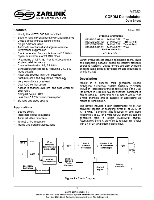
Ordering InformationMT352/CG/GP1N 64 Pin LQFP TraysMT352/CG/GP1Q 64 Pin LQFP Tape & Reel MT352/CG/GP2Q 64 Pin LQFP*Tape & Reel MT352/CG/GP2N 64 Pin LQFP*Trays* Pb Free Matte Tin0o C to +70o CMT352COFDM DemodulatorData SheetFigure 1 - Block DiagramRF inADCAGCSecondary Tuner controlImpulse SuppressionIF to Baseband conversion &InterpolatorFFTSymbol,Carrier &Timing RecoveryPilot &Channel Processor Control engineSymbol & Bit De-interleaver & DemapperFECMPEGTS2-wire busPrimary 2-wire busMT352Data SheetUnique algorithms that actively filter out impulse noise, without affecting normal performance, have been implemented. This reduces the interference effect from vehicles and electrical appliances, which is known to have significant detrimental effect on the quality of digital TV reception.Programming is simplified utilizing a high level command driven interface. A sophisticated engine controls all acquisition and tracking operations as well as controlling the tuner via a 2-wire bus. Any frequency range can be automatically scanned for digital TV channels. This mechanism ensures minimal interaction, maximum flexibility,fastest acquisition and the fastest auto scan capability of any chip in the market.Blind acquisition mode enables automatic detection of all OFDM signal parameters, including mode, guard and spectral inversion. The frequency capture range is sufficient to compensate for the combined offset introduced by the tuner and broadcaster.The device is packaged in a 64 pin LQFP and consumes less than 220mW of power.Figure 2 - Package OutlineMT352 CG YYWW *W ∆•Pin 1 CornerMT352Data Sheet Pin DescriptionPin Description TablePin No Name Description I/O Type V mA MPEG pins47MOSTRT MPEG packet start OCMOS Tristate 3·3148MOVAL MPEG data valid O3·31 49-53, 56-58MDO(0:7)MPEG data bus O3·31 61MOCLK MPEG clock out O3·31 62BKERR Block error O3·31 63MICLK MPEG clock in I CMOS 3·311STATUS Status output O3·31 6IRQ Interrupt output O Open drain56 Control pins4CLK1Serial clock I CMOS55DATA1Serial data I/O Open drain 56 23XTI Low phase noiseoscillatorICMOS24XTO O10SLEEP Device power down I3·3 12, 15-18SADD(4:0)Serial address set I3·344SMTEST Scan mode enable I3·335CLK2/GPP0Serial clock tuner I/OOpen drain 5636DATA2/GPP1Serial data tuner I/O56 42AGC1Primary AGC O56 41AGC2/GPP2Secondary AGC I/O56 43GPP(3)General purpose I/O I/O56 9RESET Device reset I CMOS527OSCMODE Crystal oscillator mode I CMOS3·326PLLTEST PLL analogue test OAnalog inputs30VIN positive input I31VIN negative input ISupply pinsMT352Data Sheet21PLLVDD PLL supplyS 1·822PLLGND S 07, 19, 37, 39, 59, 64CVDD Core logic power S 1·82, 13, 45, 54, VDD I/O ring power S 3·31, 3, 8, 14, 20, 25, 38, 40, 46, 55, 60GND Core and I/O ground S 028AVDD ADC analog supplyS 1·829, 32AGND S 033DVDD ADC digital supply S 1·834DGNDSPin Description Table (continued)Pin NoName Description I/O TypeV mATable of ContentsFeatures . . . . . . . . . . . . . . . . . . . . . . . . . . . . . . . . . . . . . . . . . . . . . . . . . . . . . . . . . . . . . . . . . . . . . . . . . . . . . . . . . 1 Applications . . . . . . . . . . . . . . . . . . . . . . . . . . . . . . . . . . . . . . . . . . . . . . . . . . . . . . . . . . . . . . . . . . . . . . . . . . . . . 1 Description . . . . . . . . . . . . . . . . . . . . . . . . . . . . . . . . . . . . . . . . . . . . . . . . . . . . . . . . . . . . . . . . . . . . . . . . . . . . . . 1 Pin Description . . . . . . . . . . . . . . . . . . . . . . . . . . . . . . . . . . . . . . . . . . . . . . . . . . . . . . . . . . . . . . . . . . . . . . . . . . . 3 1.0 Functional Description . . . . . . . . . . . . . . . . . . . . . . . . . . . . . . . . . . . . . . . . . . . . . . . . . . . . . . . . . . . . . . . . . .81.1 Analogue-to-Digital Converter. . . . . . . . . . . . . . . . . . . . . . . . . . . . . . . . . . . . . . . . . . . . . . . . . . . . . . . . . . .91.2 Automatic Gain Control. . . . . . . . . . . . . . . . . . . . . . . . . . . . . . . . . . . . . . . . . . . . . . . . . . . . . . . . . . . . . . . .91.3 IF to Baseband Conversion. . . . . . . . . . . . . . . . . . . . . . . . . . . . . . . . . . . . . . . . . . . . . . . . . . . . . . . . . . . . .91.4 Adjacent Channel Filtering . . . . . . . . . . . . . . . . . . . . . . . . . . . . . . . . . . . . . . . . . . . . . . . . . . . . . . . . . . . .101.5 Interpolation and Clock Synchronisation. . . . . . . . . . . . . . . . . . . . . . . . . . . . . . . . . . . . . . . . . . . . . . . . . .101.6 Carrier Frequency Synchronisation. . . . . . . . . . . . . . . . . . . . . . . . . . . . . . . . . . . . . . . . . . . . . . . . . . . . . .101.7 Symbol Timing Synchronisation . . . . . . . . . . . . . . . . . . . . . . . . . . . . . . . . . . . . . . . . . . . . . . . . . . . . . . . .101.8 Fast Fourier Transform . . . . . . . . . . . . . . . . . . . . . . . . . . . . . . . . . . . . . . . . . . . . . . . . . . . . . . . . . . . . . . .101.9 Common Phase Error Correction . . . . . . . . . . . . . . . . . . . . . . . . . . . . . . . . . . . . . . . . . . . . . . . . . . . . . . .101.10 Channel Equalisation . . . . . . . . . . . . . . . . . . . . . . . . . . . . . . . . . . . . . . . . . . . . . . . . . . . . . . . . . . . . . . .101.11 Impulse Filtering . . . . . . . . . . . . . . . . . . . . . . . . . . . . . . . . . . . . . . . . . . . . . . . . . . . . . . . . . . . . . . . . . . .101.12 Transmission Parameter Signalling (TPS) . . . . . . . . . . . . . . . . . . . . . . . . . . . . . . . . . . . . . . . . . . . . . . .111.13 De-Mapper. . . . . . . . . . . . . . . . . . . . . . . . . . . . . . . . . . . . . . . . . . . . . . . . . . . . . . . . . . . . . . . . . . . . . . . .111.14 Symbol and Bit De-Interleaving. . . . . . . . . . . . . . . . . . . . . . . . . . . . . . . . . . . . . . . . . . . . . . . . . . . . . . . .111.15 Viterbi Decoder . . . . . . . . . . . . . . . . . . . . . . . . . . . . . . . . . . . . . . . . . . . . . . . . . . . . . . . . . . . . . . . . . . . .111.16 MPEG Frame Aligner . . . . . . . . . . . . . . . . . . . . . . . . . . . . . . . . . . . . . . . . . . . . . . . . . . . . . . . . . . . . . . .111.17 De-interleaver . . . . . . . . . . . . . . . . . . . . . . . . . . . . . . . . . . . . . . . . . . . . . . . . . . . . . . . . . . . . . . . . . . . . .111.18 Reed-Solomon Decoder . . . . . . . . . . . . . . . . . . . . . . . . . . . . . . . . . . . . . . . . . . . . . . . . . . . . . . . . . . . . .111.19 De-scrambler. . . . . . . . . . . . . . . . . . . . . . . . . . . . . . . . . . . . . . . . . . . . . . . . . . . . . . . . . . . . . . . . . . . . . .121.20 MPEG Transport Interface. . . . . . . . . . . . . . . . . . . . . . . . . . . . . . . . . . . . . . . . . . . . . . . . . . . . . . . . . . . .122.0 Software control. . . . . . . . . . . . . . . . . . . . . . . . . . . . . . . . . . . . . . . . . . . . . . . . . . . . . . . . . . . . . . . . . . . . . . .123.0 Interfaces . . . . . . . . . . . . . . . . . . . . . . . . . . . . . . . . . . . . . . . . . . . . . . . . . . . . . . . . . . . . . . . . . . . . . . . . . . . .123.1 2-Wire Bus. . . . . . . . . . . . . . . . . . . . . . . . . . . . . . . . . . . . . . . . . . . . . . . . . . . . . . . . . . . . . . . . . . . . . . . . .133.2 Host. . . . . . . . . . . . . . . . . . . . . . . . . . . . . . . . . . . . . . . . . . . . . . . . . . . . . . . . . . . . . . . . . . . . . . . . . . . . . .133.2.1 Tuner . . . . . . . . . . . . . . . . . . . . . . . . . . . . . . . . . . . . . . . . . . . . . . . . . . . . . . . . . . . . . . . . . . . . . . . .133.2.2 Examples of 2-Wire Bus Messages. . . . . . . . . . . . . . . . . . . . . . . . . . . . . . . . . . . . . . . . . . . . . . . . .143.2.3 Primary 2-Wire Bus Timing . . . . . . . . . . . . . . . . . . . . . . . . . . . . . . . . . . . . . . . . . . . . . . . . . . . . . . .143.3 MPEG . . . . . . . . . . . . . . . . . . . . . . . . . . . . . . . . . . . . . . . . . . . . . . . . . . . . . . . . . . . . . . . . . . . . . . . . . . . .153.3.1 Data Output Header Format. . . . . . . . . . . . . . . . . . . . . . . . . . . . . . . . . . . . . . . . . . . . . . . . . . . . . . .153.3.2 MPEG data output signals. . . . . . . . . . . . . . . . . . . . . . . . . . . . . . . . . . . . . . . . . . . . . . . . . . . . . . . .163.3.3 MPEG Output Timing. . . . . . . . . . . . . . . . . . . . . . . . . . . . . . . . . . . . . . . . . . . . . . . . . . . . . . . . . . . .163.3.3.1 MOCLKINV = 1. . . . . . . . . . . . . . . . . . . . . . . . . . . . . . . . . . . . . . . . . . . . . . . . . . . . . . . . . . . .173.3.3.2 MOCLKINV = 0. . . . . . . . . . . . . . . . . . . . . . . . . . . . . . . . . . . . . . . . . . . . . . . . . . . . . . . . . . . .174.0 Electrical Characteristics . . . . . . . . . . . . . . . . . . . . . . . . . . . . . . . . . . . . . . . . . . . . . . . . . . . . . . . . . . . . . . .194.1 Recommended Operating Conditions. . . . . . . . . . . . . . . . . . . . . . . . . . . . . . . . . . . . . . . . . . . . . . . . . . . .194.2 Absolute maximum ratings . . . . . . . . . . . . . . . . . . . . . . . . . . . . . . . . . . . . . . . . . . . . . . . . . . . . . . . . . . . .194.3 DC Electrical Characteristics . . . . . . . . . . . . . . . . . . . . . . . . . . . . . . . . . . . . . . . . . . . . . . . . . . . . . . . . . .204.4 Crystal Specification and External Clocking . . . . . . . . . . . . . . . . . . . . . . . . . . . . . . . . . . . . . . . . . . . . . . .215.0 Application Circuit. . . . . . . . . . . . . . . . . . . . . . . . . . . . . . . . . . . . . . . . . . . . . . . . . . . . . . . . . . . . . . . . . . . . .22Figure 1 - Block Diagram. . . . . . . . . . . . . . . . . . . . . . . . . . . . . . . . . . . . . . . . . . . . . . . . . . . . . . . . . . . . . . . . . . . . . 1 Figure 2 - Package Outline . . . . . . . . . . . . . . . . . . . . . . . . . . . . . . . . . . . . . . . . . . . . . . . . . . . . . . . . . . . . . . . . . . . 2 Figure 3 - OFDM Demodulator Diagram . . . . . . . . . . . . . . . . . . . . . . . . . . . . . . . . . . . . . . . . . . . . . . . . . . . . . . . . . 8 Figure 4 - FEC Block Diagram. . . . . . . . . . . . . . . . . . . . . . . . . . . . . . . . . . . . . . . . . . . . . . . . . . . . . . . . . . . . . . . . . 8 Figure 5 - Primary Interfaces. . . . . . . . . . . . . . . . . . . . . . . . . . . . . . . . . . . . . . . . . . . . . . . . . . . . . . . . . . . . . . . . . 12 Figure 6 - Primary 2-Wire Bus Timing . . . . . . . . . . . . . . . . . . . . . . . . . . . . . . . . . . . . . . . . . . . . . . . . . . . . . . . . . . 14 Figure 7 - DVB Transport Packet Header Byte . . . . . . . . . . . . . . . . . . . . . . . . . . . . . . . . . . . . . . . . . . . . . . . . . . . 15 Figure 8 - MPEG Output Data Waveforms. . . . . . . . . . . . . . . . . . . . . . . . . . . . . . . . . . . . . . . . . . . . . . . . . . . . . . . 16 Figure 9 - MPEG Timing - MOCLKINV = 1 . . . . . . . . . . . . . . . . . . . . . . . . . . . . . . . . . . . . . . . . . . . . . . . . . . . . . . 17 Figure 10 - MPEG Timing - MOCLKINV = 0 . . . . . . . . . . . . . . . . . . . . . . . . . . . . . . . . . . . . . . . . . . . . . . . . . . . . . 18 Figure 11 - Crystal Oscillator Circuit. . . . . . . . . . . . . . . . . . . . . . . . . . . . . . . . . . . . . . . . . . . . . . . . . . . . . . . . . . . . 21 Figure 12 - Typical Application Circuit . . . . . . . . . . . . . . . . . . . . . . . . . . . . . . . . . . . . . . . . . . . . . . . . . . . . . . . . . . 22Table 1 - Programmable Address Details for 2-Wire Bus in TNIM Evaluation Application. . . . . . . . . . . . . . . . . . . 13 Table 2 - Timing of 2-Wire Bus. . . . . . . . . . . . . . . . . . . . . . . . . . . . . . . . . . . . . . . . . . . . . . . . . . . . . . . . . . . . . . . . 15 Table 3 - MOCLKINV = 1. . . . . . . . . . . . . . . . . . . . . . . . . . . . . . . . . . . . . . . . . . . . . . . . . . . . . . . . . . . . . . . . . . . . 17 Table 4 - MDOSWAP = 0. . . . . . . . . . . . . . . . . . . . . . . . . . . . . . . . . . . . . . . . . . . . . . . . . . . . . . . . . . . . . . . . . . . . 17 Table 5 - MDOSWAP = 1. . . . . . . . . . . . . . . . . . . . . . . . . . . . . . . . . . . . . . . . . . . . . . . . . . . . . . . . . . . . . . . . . . . . 181.0 Functional DescriptionA functional block diagram of the MT352 OFDM demodulator is shown in Figure 3. This accepts an IF analogue signal and delivers a stream of demodulated soft decision data to the on-chip Viterbi decoder. Clock, timing and frequency synchronization operations are all digital and there are no analogue control loops except the AGC. The frequency capture range is large enough for all practical applications. This demodulator has novel algorithms to combat impulse noise as well as co-channel and adjacent channel interference. If the modulation is hierarchical, the OFDM outputs both high and low priority data streams. Only one of these streams is FEC-decoded, but the FEC can be switched from one stream to another with minimal interruption to the transport stream.Figure 3 - OFDM Demodulator DiagramThe FEC module shown in Figure 4 consists of a concatenated convolutional (Viterbi) and Reed-Solomon decoder separated by a depth-12 convolutional de-interleaver. The Viterbi decoder operates on 5-bit soft decisions to provide the best performance over a wide range of channel conditions. The trace-back depth of 128 ensures minimum loss of performance due to inevitable survivor truncation, especially at high code rates. Both the Viterbi and Reed-Solomon decoders are equipped with bit-error monitors. The former provides the bit error rate (BER) at the OFDM output. The latter is the more useful measure as it gives the Viterbi output BER. The error collecting intervals of these are programmable over a very wide range.Figure 4 - FEC Block DiagramThe FSM controller shown in Figure 3 above controls both the demodulator and the FEC. It also drives the 2-wire bus to the tuner. The controller facilitates the automated search of all parameters or any sub-set of parameters of the received signal. It can also be used to scan any defined frequency range searching for OFDM channels. Thismechanism provides the fast channel scan and acquisition performance, whilst requiring minimal software overhead in the host driver.The algorithms and architectures used in the MT352 have been heavily optimized to minimize hardware and chip area. This is proven by its 220mW (typical) power consumption, which is the lowest of any OFDM device in the market today.1.1 Analogue-to-Digital ConverterThe MT352 has a high performance 10-bit analogue-to-digital converter (ADC) which can sample a 6, 7 or 8MHz bandwidth OFDM signal, with its spectrum centred at:• 4.57MHz near-zero IF•36.17MHz IF•43.75MHz IFThe ADC can be clocked using:•Crystal oscillator with a 20.48MHz crystal• 4 MHz or 27MHz clock inputAn on-chip programmable phase locked loop (PLL) is used to generate the ADC sampling clock. The crystal frequency of 20.48MHz is used for 36.17MHz IF sampling and 19.6267MHz is used for 43.75MHz IF sampling. Note that this 19.6267MHz sampling clock can be generated from the 20.48MHz crystal by appropriately programming the PLL. Hence the same 20.48MHz crystal can support 6, 7 and 8MHz OFDM as well as 36.17 and 43.75MHz IF.1.2 Automatic Gain ControlAn AGC module compares the absolute value of the digitized signal with a programmable reference. The error signal is filtered and is used to control the gain of the amplifier. A sigma-delta modulated output is provided, which has to be RC low-pass filtered to obtain the voltage to control the amplifier. Upper and lower limits can be set to the AGC control voltage using registers.The programmable AGC reference has been optimized. A large value for the reference leads to excessive ADC clipping and a small value results in excessive quantization noise. Hence the optimum value has been determined assuming the input signal amplitude to be Gaussian distributed. The latter is justified by applying the central limit theorem in statistics to the OFDM signal, which consists of a large number of randomly modulated carriers. This reference or target value may have to be lowered slightly for some applications. Slope control bits have been provided for the AGCs and these have to be set correctly depending on the Gain-versus-Voltage slope of the gain control amplifiers.The bandwidth of the AGC is set to a large value for quick acquisition then reduced to a small value for tracking. The AGC is free running during OFDM channel changes and locks to the new channel while the tuner lock is being established. This is one of the features of MT352 used to minimize acquisition time. A robust AGC lock mechanism is provided and the other parts of the MT352 begin to acquire only after the AGC has locked. Two AGC control outputs are available, one to drive an RF amplifier and the other to control an IF amplifier. The parameters for both loops are programmable. In the default mode, only the IF AGC loop is activated.1.3 IF to Baseband ConversionSampling a 36.17MHz IF signal at 20.48MHz results in a spectrally inverted OFDM signal centred at 4.79MHz. Sampling a 43.75MHz IF signal at 19.6267MHz gives a non-inverted signal at 4.5MHz. The first step of the demodulation process is to convert this signal to a complex (in-phase and quadrature) signal in baseband. A correction for spectral inversion is implemented during this conversion process. Note also that the MT352 has control mechanisms to search automatically for an unknown spectral inversion status.1.4 Adjacent Channel FilteringAdjacent channels, in particular the Nicam digital sound signal associated with analogue channels, are filtered prior to the FFT.1.5 Interpolation and Clock SynchronisationMT352 uses digital timing recovery and this eliminates the need for an external VCXO. The ADC samples the signal at a fixed rate, for example, 20.48MHz. Conversion of the 20.48MHz signal to the OFDM sample rate is achieved using the time-varying interpolator. The OFDM sample rate is 64/7MHz for 8 MHz and this is scaled by factors 6/8 and 7/8 for 6 and 7MHz channel bandwidths. The nominal ratio of the ADC to OFDM sample rate is programmed in a MT352 register (defaults are for 20.48MHz sampling and 8MHz OFDM). The clock recovery phase locked loop in the MT352 compensates for inaccuracies in this ratio due to uncertainties of the frequency of the sampling clock.1.6 Carrier Frequency SynchronisationThere can be frequency offsets in the signal at the input to OFDM, partly due to tuner step size and partly due to broadcast frequency shifts, typically 1/6MHz. These are tracked out digitally, without the need for an analogue frequency control (AFC) loop.The default frequency capture range has been set to ±285kHz in the 2K mode and ±142kHz in the 8K mode. However, these values can be doubled, if necessary, by programming an on-chip register. It is recommended that this larger capture range be used for channel scan in order to find channels with broadcast frequency shifts, without having to adjust the tuner.After the OFDM module has locked, the frequency offset can be read from an on-chip register.1.7 Symbol Timing SynchronisationThis module computes the optimum sample position to trigger the FFT in order to eliminate or minimize inter-symbol interference in the presence of multi-path distortion. Furthermore, this trigger point is continuously updated to dynamically adapt to time-variations in the transmission channel.1.8 Fast Fourier TransformThe FFT module uses the trigger information from the timing synchronization module to set the start point for an FFT. It then uses either a 2K or 8K FFT to transform the data from the time domain to the frequency domain. An extremely hardware-efficient and highly accurate algorithm has been used for this purpose.1.9 Common Phase Error CorrectionThis module subtracts the common phase offset from all the carriers of the OFDM signal to minimize the effect of the tuner phase noise on system performance.1.10 Channel EqualisationThis consists of two parts. The first part involves estimating the channel frequency response from pilot information. Efficient algorithms have been used to track time-varying channels with a minimum of hardware. The second part involves applying a correction to the data carriers based on the estimated frequency response of the channel. This module also generates dynamic channel state information (CSI) for every carrier in every symbol.1.11 Impulse FilteringMT352 contains several mechanisms to reduce the impact of impulse noise on system performance.1.12 Transmission Parameter Signalling (TPS)An OFDM frame consists of 68 symbols and a superframe is made up of four such frames. There is a set of TPS carriers in every symbol and all these carry one bit of TPS. These bits, when combined, include information about the transmission mode, guard ratio, constellation, hierarchy and code rate, as defined in ETS 300 744. In addition, the first eight bits of the cell identifier are contained in even frames and the second eight bits of the cell identifier are in odd frames. The TPS module extracts all the TPS data, and presents these to the host processor in a structured manner.1.13 De-MapperThis module generates soft decisions for demodulated bits using the channel-equalized in-phase and quadrature components of the data carriers as well as per-carrier channel state information (CSI). The de-mapping algorithm depends on the constellation (QPSK, 16QAM or 64QAM) and the hierarchy α = 0, 1, 2 or 3). Soft decisions for both low- and high-priority data streams are generated.1.14 Symbol and Bit De-InterleavingThe OFDM transmitter interleaves the bits within each carrier and also the carriers within each symbol. The de-interleaver modules consist largely of memory to invert these interleaving functions and present the soft decisions to the FEC in the original order.1.15 Viterbi DecoderThe Viterbi decoder accepts the 5-bit soft decision data from the OFDM demodulator and outputs a decoded bit-stream. The decoder does the de-puncturing of the input data for all code rates other than 1/2. It then evaluates the branch metrics and passes these to a 64-state path-metric updating unit, which in turn outputs a 64-bit word to the survivor memory. The Viterbi decoded bits are obtained by tracing back the survivor paths in this memory. A trace-back depth of 128 is used to minimize any loss in performance, especially at high code rates.The decoder re-encodes the decoded bits and compares these with received data (delayed) to compute bit errors at its input, on the assumption that the Viterbi output BER is significantly lower than its input BER.1.16 MPEG Frame AlignerThe Viterbi decoded bit stream is aligned into 204-byte frames. A robust synchronization algorithm is used to ensure correct lock and to prevent loss of lock due to noise impulses.1.17 De-interleaverErrors at the Viterbi output occur in bursts and the function of the de-interleaver is to spread these errors over a number of 204-byte frames to give the Reed-Solomon decoder a better chance of correcting these. The de-interleaver is a memory unit which implements the inverse of the convolutional interleaving function introduced by the transmitter.1.18 Reed-Solomon DecoderEvery 188-byte transport packet is encoded by the transmitter into a 204-byte frame, using a truncated version of a systematic (255,239) Reed-Solomon code. The corresponding (204,188) Reed-Solomon decoder is capable of correcting up to eight byte errors in a 204-byte frame. It may also detect frames with more than eight byte errors. In addition to efficiently performing this decoding function, the Reed-Solomon decoder in MT352 keeps a count of the number of bit errors corrected over a programmable period and the number of uncorrectable blocks. This information can be used to compute the post-Viterbi BER.1.19 De-scramblerThe de-scrambler de-randomizes the Reed-Solomon decoded data by generating the exclusive-OR of this with a pseudo-random bit sequence (PRBS). This outputs 188-byte MPEG transports packets. The TEI bit of the packet header is set to indicate uncorrectable packets.1.20 MPEG Transport InterfaceMPEG data can be output in parallel or serial mode. The output clock frequency is automatically chosen to present the MPEG data as uniformly spaced as possible to the transport processor. This frequency depends on the guard ratio, constellation, hierarchy and code rate. There is also an option for the data to be extracted from the MT352 with a clock provided by the user.2.0 Software controlAcquisition of an OFDM channel and frequency scan for OFDM channels are controlled by an on-chip state machine, which minimizes the software requirement in the host processor. To acquire a channel, the host programs the channel frequency in the MT352. The on-chip state machine then writes the frequency information to the tuner, awaits tuner lock and acquires the OFDM channel to generate the transport stream. The controller can be made to automatically search for every parameter in the OFDM signal, including spectral inversion status. Furthermore, this controller will re-acquire the channel in the event of an interruption to the incoming signal.To scan a frequency range, the host programs the start and end frequencies for the search as well as the step size, which defaults to 8 MHz. The MT352 then automatically scans the frequency range by appropriately programming the tuner and searching for OFDM signals. Once a channel has been located, the host is interrupted to read the channel information from the MT352. Then MT352 continues the search. By default, only the channels which can generate a reliable transport stream are reported, but there is also provision for locating very weak channels. The frequency capture range of MT352 can be maximized to capture channels with frequency offsets without re-programming the tuner, in both 2K and 8K modes.The above approach to channel acquisition and scan has resulted in very fast acquisition and scan times whilst minimizing software overhead in the host processor. Furthermore, all this functionality has very efficiently been mapped into hardware to result in a device consuming less than 220mW of power.3.0 InterfacesFigure 5 - Primary InterfacesThe MT352 interfaces to other parts of a terrestrial receiver system can be partitioned into three groups: the host controller, the tuner and the MPEG decoder. One other pin, the Status output, is multi-functional and can directlydrive a LED to show the status of a range of different internal lock flags. Alternatively, it can drive an audio transducer to give an audio frequency that is dependent upon the error rate of the received signal.This feature can be used for faster installation of a system where the aerial may need to be adjusted, as signal strength is not the best guide for the optimum aerial position for COFDM reception.3.1 2-Wire Bus3.2 HostThe primary 2-wire bus serial interface uses pins:•DATA1 (pin 5) serial data, the most significant bit is sent first.•CLK1 (pin 4) serial clock.The 2-wire bus address is determined by applying VDD or VSS to the SADD[4:0] pins.In the current TNIM evaluation application, the 2-wire bus address is 0001 111 R/ W with the pins connected as follows:ADDR[7] ADDR[6] ADDR[5] ADDR[4] ADDR[3] ADDR[2] ADDR[1]Not programmable SADD[4] SADD[3] SADD[2] SADD[1] SADD[0]VSS VSS VSS VDD VDD VDD VDD Table 1 - Programmable Address Details for 2-Wire Bus in TNIM Evaluation ApplicationWhen the MT352 is powered up, the RESET pin 28 should be held low for at least 50ms after VDD has reached normal operation levels. As the RESET pin goes high, the logic levels on SADD[4:0] are latched as the 2-wire bus address. ADDR[0] is the R/ W bit.The circuit works as a slave transmitter with the lsb set high or as a slave receiver with the lsb set low. In receive mode, the first data byte is written to the RADD virtual register, which forms the register sub-address. The RADD register takes an 8-bit value that determines which of 256 possible register addresses is written to by the following byte. Not all addresses are valid and many are reserved registers that must not be changed from their default values. Multiple byte reads or writes will auto-increment the value in RADD, but care should be taken not to access the reserved registers accidentally.Following a valid chip address, the 2-wire bus STOP command resets the RADD register to 00. If the chip address is not recognized, the MT352 will ignore all activity until a valid chip address is received. The 2-wire bus START command does NOT reset the RADD register to 00. This allows a combined 2-wire bus message, to point to a particular read register with a write command, followed immediately with a read data command. If required, this could next be followed with a write command to continue from the latest address. RADD would not be sent in this case. Finally, a STOP command should be sent to free the bus.When the 2-wire bus is addressed (after a recognized STOP command) with the read bit set, the first byte read out is the contents of register 00.3.2.1 TunerThe MT352 has a General Purpose Port that can be configured to provide a secondary 2-wire bus. Master control mode is selected by a single register control bit.The allocation of the pins is: GPP0 pin 35 = CLK2, GPP1 pin 36 = DATA2.。
RCR-650A iVD650 产品说明书
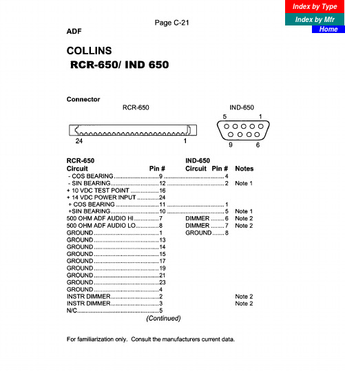
For familiarization only. Consult the manufacturers current data.
volts out 13 to voltage converter, 14 volts in 25. 4. For 14 volts, 48 to Dimmer, 20 ground. For 28 volts, 20 to Dimmer, 18 open.
Index by Type
Index by Mfr Home
N/C.. ..............................................
.6
SENSE ANTENNA ......................... 18
X LOOP ANTENNA.. ..................... .22
Y LOOP ANTENNA.. ..................... .20
20
N/C.. ...............................................
I
N/C.. ..............................................
.I0
N/C.. ..............................................
Notes 1. For top mount antenna, reverse 2. For 14 volts, 7 and 3 to Dimmer,
Dimmer, 7 and 3 open.
2 and 5. 6 and 2 to ground.
For 28 volts, 6 and 2 to
E53NA50中文资料

E53NA50中文资料STE53NA50N -CHANNEL ENHANCEMENT MODEFAST POWER MOS TRANSISTORs TYPICAL R DS(on)=0.075?s HIGH CURRENT POWER MODULE s AVALANCHE RUGGED TECHNOLOGYsVERY LARGE SOA -LARGE PEAK POWER CAPABILITYs EASY TO MOUNTsSAME CURRENT CAPABILITY FOR THE TWO SOURCE TERMINALSs EXTREMELY LOW Rth (Junction to case)sVERY LOW INTERNAL PARASITIC INDUCTANCEsISOLATED PACKAGE UL RECOGNIZEDAPPLICATIONS s SMPS &UPS s MOTOR CONTROL s WELDING EQUIPMENT s OUTPUT STAGE FOR PWM,ULTRASONIC CIRCUITSINTERNAL SCHEMATIC DIAGRAMFebruary 1998ABSOLUTE MAXIMUM RATINGSSymbol ParameterValue Unit V DS Drain-source Voltage (V GS =0)500V V DGR Drain-gate Voltage (R GS =20k ?)500V V GS Gate-source Voltage ±30V I D Drain Current (continuous)at T c =25oC 53A ID Drain Current (continuous)at T c =100o C 33A I DM(?)Drain Current (pulsed)212A P to t Total Dissipation at T c =25oC 460W Derating Factor 3.68W/o CT st g Storage Temperature-55to 150o C T j Max.Operating Junction Temperature 150oCV ISOInsulation Withhstand Voltage (AC-RMS)2500V (?)Pulse width limited by safe operating areaTYPE V DSS R DS(on)I D STE53NA50500V<0.085?53AISOTOP1/7THERMAL DATAR t hj-ca se R thc-h Thermal Resistance Junction-case Max Thermal Resistance Case-heatsink With ConductiveGrease Applied Max0.270.05o C/Wo C/WAVALANCHE CHARACTERISTICSSymbol Parameter Max Value UnitI AR Avalanche Current,Repetitive or Not-Repetitive(pulse width limited by T j max,δ <1%)26AE AS Single Pulse Avalanche Energy(starting T j=25o C,I D=I AR,V DD=50V)1014mJELECTRICAL CHARACTERISTICS(T case=25o C unless otherwise specified)OFFSymbol Parameter Test Conditions Min.Typ.Max.Unit V(BR)DSS Drain-sourceBreakdown VoltageI D=1mA V GS=0500VI DSS Zero Gate VoltageDrain Current(V GS=0)V DS=Max RatingV DS=Max Rating T c=125o C1001000μAμAI GSS Gate-body LeakageCurrent(V DS=0)V GS=±30V±400nA ON(?)Symbol Parameter Test Conditions Min.Typ.Max.Unit V GS(th)Gate ThresholdVoltageV DS=V GS I D=1mA 2.253 3.75VR DS(on)Static Drain-source OnResistanceV GS=10V I D=27A0.0750.085?I D(o n)On State Drain Current V DS>I D(on)x R DS(on)maxV GS=10V53A DYNAMICSymbol Parameter Test Conditions Min.Typ.Max.Unit g fs(?)ForwardTransconductanceV DS>I D(on)X RDS(on)MAX I D=27A25SC iss C oss C rss Input CapacitanceOutput CapacitanceReverse TransferCapacitanceV DS=25V f=1MHz V GS=0131500450162000650nFpFpFSTE53NA50 2/7ELECTRICAL CHARACTERISTICS(continued) SWITCHING ONSymbol Parameter Test Conditions Min.Typ.Max.Unit t d(on) t r Turn-on TimeRise TimeV DD=250V I D=27AR G=4.7 ?V GS=10V(see test circuit,figure1)579280130nsnsQ g Q gs Q gd Total Gate ChargeGate-Source ChargeGate-Drain ChargeV DD=400V I D=53A V GS=10V47054219658nCnCnCSWITCHING OFFSymbol Parameter Test Conditions Min.Typ.Max.Unit t r(Vof f) t ft c Off-voltage Rise TimeFall TimeCross-over TimeV DD=400V I D=53AR G=4.7 ?V GS=10V(see test circuit,figure3)1053614514550205nsnsnsSOURCE DRAIN DIODESymbol Parameter Test Conditions Min.Typ.Max.Unit I SD I SDM(?)Source-drain CurrentSource-drain Current(pulsed)53212AAV SD(?)Forward On Voltage I SD=53A V GS=0 1.6V t rr Q rr I RRM Reverse RecoveryTimeReverse RecoveryChargeReverse RecoveryCurrentI SD=53A di/dt=100A/μsV R=100V T j=150o C(see test circuit,figure3)100031.563nsμCA(?)Pulsed:Pulse duration=300μs,duty cycle1.5% (?)Pulse width limited by safe operating areaSafe Operating Area for Thermal ImpedanceSTE53NA503/7Output Characteristics TransconductanceGate Charge vs Gate-source Voltage Transfer Characteristics Static Drain-source On Resistance Capacitance VariationsSTE53NA50 4/7Normalized Gate Threshold Voltage vs TemperatureSource-drain Diode Forward Characteristics Fig.2:Gate Charge test Circuit Normalized On Resistance vs Temperature Fig.1:Switching Times Test Circuits For Resistive Load Fig.3:Test Circuit For Inductive Load Switching And Diode Recovery TimesSTE53NA505/7DIM.mm inch MIN.TYP.MAX.MIN.TYP.MAX.A 11.812.20.4660.480B 8.99.10.3500.358C 1.95 2.050.0760.080D 0.750.850.0290.033E 12.612.80.4960.503F 25.1525.50.990 1.003G 31.531.71.240 1.248H 40.157J 4.1 4.30.1610.169K 14.915.10.5860.594L 30.130.31.185 1.193M 37.838.21.488 1.503N 40.157O7.88.20.3070.322BEHONJ K L MFACGDISOTOP MECHANICAL DATASTE53NA506/7Information furnished is believed to be accurate and reliable.However,SGS-THOMSON Microelectronics assumes no responsability for the consequences of use of such information nor for any infringement of patents or other rights of third parties which may results from its use.No license is granted by implication or otherwise under any patent or patent rights of SGS-THOMSON Microelectronics.Specifications mentioned in this publication are subject to change without notice.This publication supersedes and replaces all information previously supplied.SGS-THOMSON Microelectronics products are not authorized for use as critical components in life support devices or systems without express written approval of SGS-THOMSON Microelectonics.1998SGS-THOMSON Microelectronics -Printed in Italy -All Rights ReservedSGS-THOMSON Microelectronics GROUP OF COMPANIESAustralia -Brazil -Canada -China -France -Germany -Italy -Japan -Korea -Malaysia -Malta -Morocco -The Netherlands -Singapore -Spain -Sweden -Switzerland -Taiwan -Thailand -United Kingdom -U.S.A...STE53NA50 7/7。
RadiPower 产品手册说明书

Models: RPR3006W RadiPower ®Product ManualRF Power MetersPage 2 of 19RadiPower® product manualThis product manual pertains to the RadiPower®.Models: RPR3006W - RPR3008W - By Raditeq 16/08/21All trademarks used in this manual are the property of their respective ownersSupplier InformationRaditeq B.V.Vijzelmolenlaan 33447 GX, WoerdenThe NetherlandsTel.: +31 (0)348 200 100Internet: Email: *****************Read this manual carefully before operating the product and make sure all the safety instructions are strictly followed.For your convenience, a Quick Start Guide has been added to this product. This Quick Start Guide contains the basic start-up steps and the safety warnings.Please keep the Quick Start Guide (and this regular manual) close at hand when you operate your new Raditeq product(s).Please contact your local reseller if you have any questions.Table of contentsWARNINGS & PRECAUTIONS 4 Introduction 5 The RadiPower® Series 6 Product characteristics 6 Functional description 7 The RadiPower® 3000 Series 8 Model RPR3006W 8 RadiPower® Installation 9 Stand-alone Configuration 9 Software Configuration 10 How to configure the RadiPower® in RadiMation® 10 How to connect the RadiPower® to the RadiCentre® 11 How to check whether the RadiPower® is properly connected to RadiMation® 11 Adding coupler values in RadiMation®12 Theory of operation in burst mode 13 Prefix & Communication example: 13 Remarks about the general commands 14 Stand-alone command set 14 Burst Mode 15 Specifications RPR3006W16 Warranty Conditions18Page 3 of 19WARNINGS & PRECAUTIONSRead the contents of this product manual carefully and become familiar with the safety markings, the product instructions and the handling of the system. Please refer to the applicable product manual(s) for further information regarding the operation and control of the product(s).Only Raditeq qualified maintenance personnel is allowed to perform maintenance and/or repair service on the equipment.This product® contains materials that can be recycled and reused to minimize material waste. At the ‘end-of-life’, specialized companies can dismantle the discarded system to collect the reusable and recyclable materials. If your product is at its ‘end-of-life’, please return it to your local reseller or to Raditeq for recycling.For cleaning, use a clean, dry cloth (or a damp cloth where needed) and wipe the surface of equipment.This product contains no hazardous substances as described in the RoHS Directive (2015/863/EU).This product contains embedded software, which is field upgradeable.For more information contact your local reseller or go to Page 4 of 19IntroductionThis manual contains information about the RadiPower® RPR3006W RF power meters.An accurate power meter is indispensable to perform reliable EMC measurements. The RadiPower® is a RF power meter especially designed for power measurements during EMC tests. The RadiPower® is an affordable, accurate and fast power meter. It provides accurate measurements over a wide frequency range, which enables effective measurements in accordance with the latest EMC standards.Please read this manual carefully and make sure to pay special attention to the chapters regarding your new product(s).RadiCentre® SystemThe RadiCentre® is a modular EMC/RF test system that serves as the interface between user and computer for all the RadiCentre® plug-in cards and modules.RadiMation® SoftwareRadiMation ® is the EMC software package from Raditeq used for remote controland automated testing of the RadiCentre® plug-in cards and modules and is sold separately. RadiField® Electric Field GeneratorThe patented RadiField® Triple A is no less than a revolution in EMC immunity testing.A complete paradigm shift involves a combination of high-level integration anda field combining technique, making several discrete components like combiner,coupler, power meters and cabling superfluous. This product is sold separately.RadiMationShielded USB cable Model: USB A male to USB mini B5 male.To connect the RF power sensor to a USB connector.The RadiPower® 3000 SeriesMMCX Trigger cable For measurements on multiple ports.RadiPower® RF power sensor Model: RPR3006W.Supporting documentation is supplied on a USB stick containing:•The (digital) User Manual and Quick Start Guide.•The installation of RadiMation® Free software and drivers.• Optional - The calibration certificate for the power meter.The RadiPower® RF power sensor is optimized for EMC measurements, where a high dynamic range, together with fast measurements, are required even at low power levels. Where most power sensors require long measurement times at low RF levels, the RadiPower® RF power sensor is able to perform accurate power measurements, with a high measurement speed, at power levels close to the noise floor, without the need for zero adjustment!Fast - EMC immunity measurements are time consuming. This is mainly dependent on the number of frequency points, the dwell time and the speed of the power meter. As the first two parameters are generally prescribed by standards, the only one that can be optimized is the speed of the power meter. The unprecedented detector technology of Raditeq’s power meters makes extremely fast and accurate power measurements a reality, even at low power levels.Accurate - Accuracy is another concern in addition to speed, when performing EMC measurements. The RadiPower® allows for high precision EMC measurements with a large dynamic range. Because the RadiPower® has a high accuracy over the complete band, it is suitable for measurements in accordance to automotive, military, telecom and EMC basic standards such as the IEC61000-4-3/6 standards.Simultaneous power measurements on multiple ports - The RadiPower®RPR3006W has two trigger ports (MMCX) which can be used to synchronizemultiple power meters. These power meters connected through a daisy chaintrigger each other to make time synchronized measurements. Due to this functionmeasurements of WLAN and/or MIMO devices according to the EN 300 328 andEN 301 893 standards.All necessary parameters can be set and calculated by RadiMation® Free (or ahigher version) making the setup and measurements effortless.Low measurement uncertainties - Impedance mismatches contribute to themeasurement uncertainty. The RadiPower® has a very low Standing Wave Ratio(SWR) and as a result, measurement uncertainties are low compared to othercontributions in the EMC measurement setups.Robust housingThe RadiPower® RF power sensor is mounted in a rugged metal housing to ensure a long life and excellent RF shielding. The power sensor is equipped with an N-type precision RF input connector and a mini USB-B connector for communication with a computer.Easy to use - With the USB interface the RadiPower® is easy to use. In addition, the RadiPower® can be controlled by both the RadiMation® integral EMC measurement software and any other EMC measurement packages, because all the software commands needed to control the unit are available. For ‘stand-alone use’ of the RadiPower®, RadiMation® Free measurement software is delivered with the power meters. The RadiPower® 3000 SeriesProduct characteristicsFunctional descriptionThe RadiPower® uses a high speed power detector to measure the RF signal, independent of the crest factor of the input signal waveform. The detected signal is sampled, at high speed, by a high speed ADC and the samples are processed by a powerful DSP. The sophisticated software enables unique functions, such as envelope tracing and burst logging. The table below shows which models support the different measurement modes.0 : CW1 : Peak √√2 : Envelope tracing√3 : Burst√CW modeThe RadiPower® performs RMS power measurements of CW-signals. In RMS mode the RadiPower® samples the signal at high speed. The RMS value of the power is calculated over the number of samples defined by the filter setting and can be read by a simple command. Due to the high sampling speed the number of readings is high, even at large filter settings. This mode is supported for all the RadiPower® models.Peak modePeak mode keeps track of the maximum power that is measured during a specific time interval. In PEAK mode, the “power?”-command will return the highest value that was measured since the last “power?”-command. After each cycle of the command the previous peak value is cleared,Burst modeIn burst mode, the RadiPower can measure a burst of RF power. It is even possible to measure a burst on multiple powermeters at the sime time (using the MMCX trigger ports). The power readings of each powermeter can be combined to a total power by RadiMation according to the EN 300 328 and EN 301 893 standards..In this mode the sample speed can be set to either 1 MS/s or 5 MS/s. The RadiPower can store a total of 100.000 bursts and is independent of the observation time. The stored data of a single burst consists of the RMS power and the start/stop-time of the burst. The start and stop time are defined by how long the power was higher than the threshold value. The threshold value can be set in RadiMation.The RMS power of a burst is calculated according to the following formula:Where m is the number of RMS power samples within the start and stop time. When measuring on a MIMO device with more than one port. It is possible to use multiple power meters. The burst values of each power meter can be combined to a single RF power using RadiMaiton. This can also be done manual by using the following formula:i is the number of power metersIt is also possible to add corrections for the coupler, beamforming gain (Y) and the assembly gain (G) of the DUT. RadiMation can compensate for these values.Connect the RadiPower® sensor to a Windows computer with a USB port for ‘stand-alone’ use. Use the supplied USB cable to connect the sensor to your computer. Windows will prompt that new hardware has been found. The USB-driver for the RadiPower® is Windows certified and will be loaded automatically from the Windows update. If the drivers are not loaded automatically, these can be installed manually from the supplied USB-key. Follow the normal instructions from Windows to install the drivers manually.Once the drivers are loaded successfully, the RadiPower® will be shown in the device list.RadiPower® InstallationStand-alone Configuration Connect the RadiPower® sensor to a Windows computer with a USB 2.0 compatible port. Use the supplied USB cable to connect the RadiPower® sensor. The hardware installation for the RadiPower® sensor is now complete.Software ConfigurationIn order to control the RadiPower® from a computer, the RadiMation® EMC software package can be used. RadiMation® from Raditeq is sold separately. A free version of RadiMation® is available on: https://www. /automated-emc-software/radimation-free/.If the RadiPower® is operated manually, this chapter can be skipped.The RadiPower® device driver is part of the Power Meter Device Driver familyHow to configure the RadiPower® in RadiMation®1. Start the latest version of RadiMation®; https:///radimation-download/2. Select the button ‘Device’ at the top menu bar, followed by clicking ‘Configure’;3. In the configuration screen select ‘Device Drivers’ and Select ‘Power meter’ or any of the otherdrivers as driver type;4. Click the ‘Add’ button to open the selection of available drivers in RadiMation®;5. Enter ‘RadiPower’ in the search bar which will show all available RadiPower® drivers;6. Select the correct driver, double click it (Optional, rename it) and press ‘OK’.2354How to check whether the RadiPower® is properly connected to RadiMation®1. Select ‘Devices’ in the top menu bar2. Open ‘Device Drivers’ and select device driver type: ‘Power Meter’3. Double click the recently configured RadiPower® or click ‘Edit’.4. Finally select the ‘Check’ button on the right side of the opened screen.5. When correctly configured, RadiMation® will notify you that the device is correctly installed.23Adding coupler values in RadiMation®In a MIMO test setup, power measurements are often performed using a coupler on the antenna port. Coupling factors can be compensated by RadiMation® using a correction file. If no couplers or additional attenuators are used in the setup, there is no need to create and apply these correction files.To create a correction file, select “File” – “New” – “Correction” from the menu bar.Press “Colums/units” to create to columns for Frequency and Attenuation.To create a constant correction versus frequency:• Press “Add Row” and enter the lowest frequency with the corresponding attenuation.• Press “Add Row” again and enter the highest frequency with the corresponding attenuation.If calibration data of the coupler is available, this data can be used to create an accurate correction for the coupler.After all data has been entered, select “File” – “Save Correction As” to save the data.Next, the correction data of the coupler has to be added to the correct power meter. Select “Configuration” and “Configuration” again. In the Configuration window select the “Device drivers” tab and select the power meter for which the correction has to be added. Press “Edit”.Press the “file open”- button in de Correction Files area to select the correction file. Perform this procedure for each power meter for which a coupler correction has to be added. RadiMation® will now automatically calculate the power values, including the coupler values.Stand-alone command setCommunication with the RadiPower® sensor is possible using a virtual COM-port (VCP)For more information see chapter ‘stand alone configuration’.NOTE: All commands can be found in the RadiCentre® Manual under the programming manual.Specifications RPR3006W & RPR3008W1. In burst mode only 1 and 5 MS/s can be set and used.• All specifications are measured after 10 minutes warm-up time and 0dBm unless specified otherwise.• T ypical specifications indicate that the measured values a re met on at least 80% of the points.• Three years warranty will be granted only after you register the product at . Without registration, a 1 year warranty period applies.For more information about the current and new Raditeq products at:T:+31348200100M:*****************W: Warranty ConditionsRaditeq B.V. offers a standard warranty term of three (3) years on their products, calculated from the shipping date, under the condition that the product is registered on . For registration of the product, the customer should provide the product model, serial number and the responsible reseller (if applicable). If the product is not registered, a limited warranty term of one (1) year will be applicable.Return Material Authorization (RMA) & Warranty repairIf a defect occurs to our product within the warranty term, a Return Material Authorization (RMA) ‘Warranty Repair’ request can be issued using the RMA link at /support. Upon receipt of the request, an RMA number will be provided. Please do not send the product without this RMA number! The defective product should be shipped to our service department at the following address:Raditeq B.V. – Service DepartmentVijzelmolenlaan 33447GX WOERDENThe NetherlandsThere will be no charge for repair services (materials or labour) within the (extended) warranty term.These warranty terms are not applicable to:• Normal wear and tear• Fibre optic cables• Products that have been improperly used• Products that have been used outside their specified range• Products that have been improperly installed and/or maintained• Products that have been modified without approval of Raditeq• Calibration and/or re-calibration of the productRepair services on products that are not covered by the Raditeq warranty will be charged to the customer.Repairs outside warrantyIf a defect is not covered under warranty, an RMA fixed-repair can be ordered on the RMA link: /support If a re-calibration is needed after repair, this calibration should be ordered separately. The calibration will be performed at the ISO17025 accredited calibration laboratories of DARE!! Calibrations, based on the applicable service code / prices. Warranty after repairFor repairs outside the original warranty period, a limited warranty of six months is applicable on the performed repair. Shipping conditions are the same as with repairs that are covered within the original warranty period.ShippingThe customer will need to arrange shipping and cover for the costs (like e.g. transportation costs, duties, taxes) for sending the defect product the service department of Raditeq in The Netherlands. Raditeq will arrange the courier and cover for the costs for the return shipment after repair.EU Declaration of Conformity WeRaditeq B.V.ofVijzelmolenlaan 3NL-3447GX WoerdenThe Netherlandsdeclare under our sole responsibility that theProduct: RadiPower® Seriesmodels: RPR3006Ware in accordance with the European directives:EMC Directive 2014/30/EULow Voltage Directive 2015/35/EURoHS Directive: 2015/863/EUper the provisions of the applicable requirements of the following harmonized standards: Emission: EN 61326-1:2013, Class A1Electrical equipment for measurement, control and laboratory use.Immunity:EN 61326-1:2013, Industrial level, performance criteria AElectrical equipment for measurement, control and laboratory use.Safety:EN 61010-1:2010, Safety requirements for electrical equipmentfor measurement, control, and laboratory useThe technical construction files are maintained at the adress specified above.Date of issue:16/08/21Place of issue:Woerden, The NetherlandsAuthorized by:P.W.J. DijkstraTitle of authority: DirectorRaditeq B.V. | Vijzelmolenlaan 3 | 3447GX Woerden | The Netherlands | T:+31 348 200 100。
麦格纳电子MT系列大功率机柜式可扩展至多兆瓦的可编程直流电源型号订购指南说明书

MT 系列大功率机柜式程控直流电源 • 可扩展至多兆瓦概述麦格纳电子设备公司的MT系列产品使用与MagnaDC程控电源产品线中的其他产品具有相同的可靠电流馈电式功率处理工艺技术和控制方式,但具有更大的功率型号:分别为100kW、150 kW和250 kW规格。
基于高频IGBT的MT系列产品是市场上单体功率最大的标准程控直流电源产品之一,与小功率型号产品相比,最大限度地减少了开关元器件的数量。
使用UID47装置可实现兆瓦功率级的扩展,该装置可提供主从控制:一个主控电源产品控制其他从机电源产品,以实现真正的系统级操作控制。
所有MT系列产品均配备额定全功率的交流输入断路器,作为额外的安全防护措施。
250 kW型号标配嵌入式12脉冲谐波中和器,确保较低THD(总谐波失真)。
通过外部附加的500kW 24脉冲或1,000 kW 48脉冲谐波中和器可获得更优质的交流波形,此项功能由麦格纳电子设100 kW 和 150 kW 型号250 kW 型号备公司为其MT系列产品专门设计和制造。
1标准型号规定纹波。
对于具有高转换速率输出(+HS)的型号,纹波更高。
详情请参考选项页。
2通过多个250 kW MT系列型号的主从并联可实现大于250 kW的功率等级。
关于此类配置的更多详情,请联系您的麦格纳电子设备公司销售代表。
第 26 页麦格纳电子设备公司第 27 页数据表 (4.4.0)MagnaDC 程控直流电源规格通过 RoHS 认证是(170.2 x 182.9 x 80.0 cm)GPIB: IEEE-488额定型号 >1000 Vdc 或具有+ISO选项的型号±6000 Vdc, 对地最大输出电压主要特性• SCPI远程编程API (应用程序界面)• 程控设置保护限制• 高精度测量 • 主从式操作功能• 快速瞬态响应• 远地感应•远程接口软件• 37-pin外部模拟量I/O接口• NI LabVIEW™IVI驱动• RS232接口• 联锁功能迅速切断输入• 可选配以太网接口和GPIB接口•在美国设计和制造可用选项• 阻流二极管(+BD)• 高隔离输出(+ISO)• 高转换速率输出(+HS)• IEEE-488 GPIB通信(+GPIB)•LXI TCP/IP以太网通信(+LXI)注:参数如有更改,恕不另行通知。
ONT-5xxOTN测试表使用手册(英文)

BN 3061/98.35 05.09 (V 4.x.x) EnglishPlease direct all enquiries to your localActerna sales company. The addressesare given at the end of this handbook.CopyrightsThis product or parts of it are based upon Recommendations and/or Standards of the Standardization Sector of the International Telecommunication Union - ITU-T and/or of the European Telecommunications Standards Institute - ETSI. These Recommendations and Standards are subject to copyrights of these organizations. Without written permission of the ITU-T and/or ETSI it is not permitted to copy ITU-T Recommendations or ETSI standards or parts thereof and/or make them available to third parties.Acterna Germany GmbHMühleweg 5, 72800 Eningen u. A.Note: Specifications, terms and conditions aresubject to change without prior notice.© Copyright 2005 Acterna, LLC.All rights reserved.Acterna, Communications T est and ManagementSolutions, and its logo are trademarks of Acterna,LLC. All other trademarks and registeredtrademarks are the property of their respectiveowners.Printed in GermanyOrder no.: BN 3061/98.35Edition: 05.09 (V 4.x.x)Previous Edition: 05.02 (V 3.x.x)Contents1OTN G.709 Test Set . . . . . . . . . . . . . . . . . . . . . . . . . . . . . . .11.1Introduction. . . . . . . . . . . . . . . . . . . . . . . . . . . . .11.2Functions. . . . . . . . . . . . . . . . . . . . . . . . . . . . . . .21.2.1Wrapper analysis. . . . . . . . . . . . . . . . . . . . . . . . .21.2.2TCM analysis. . . . . . . . . . . . . . . . . . . . . . . . . . . .21.2.3Error tests . . . . . . . . . . . . . . . . . . . . . . . . . . . . . .31.2.4Alarm tests . . . . . . . . . . . . . . . . . . . . . . . . . . . . .41.2.5Overhead analysis. . . . . . . . . . . . . . . . . . . . . . . .51.3Use of symbols and icons. . . . . . . . . . . . . . . . . .62Safety instructions. . . . . . . . . . . . . . . . . . . . . . . . . . . . . . . .92.1General safety instructionsand operating conditions. . . . . . . . . . . . . . . . . . .92.2Installation. . . . . . . . . . . . . . . . . . . . . . . . . . . . . .92.3Laser radiation. . . . . . . . . . . . . . . . . . . . . . . . . .102.4Optical surfaces. . . . . . . . . . . . . . . . . . . . . . . . .112.5Important operating instructions . . . . . . . . . . . .123Setting the Test Set . . . . . . . . . . . . . . . . . . . . . . . . . . . . . .133.1Connecting the Test Moduleto the device under test. . . . . . . . . . . . . . . . . . .133.1.1OTN Module 2.5G/2.7G FEC . . . . . . . . . . . . . .133.1.2OTN Module 10G/10.7G FEC 1550nm . . . . . .133.2Starting the OTN G.709 Test Set. . . . . . . . . . . .143.3Making the basic settings . . . . . . . . . . . . . . . . .173.3.1Setting the default values . . . . . . . . . . . . . . . . .173.3.2Manual configuration. . . . . . . . . . . . . . . . . . . . .183.3.2.1Configuration - Overview. . . . . . . . . . . . . . . . . .183.3.2.2Configuration - Interface . . . . . . . . . . . . . . . . . .18 Acterna ONT-506/512: OTN G.709iContents3.3.2.3Configuration - Test Signal(for OTN-Bulk only). . . . . . . . . . . . . . . . . . . . . . 213.3.2.4Configuration - Advanced. . . . . . . . . . . . . . . . . 223.3.2.5Configuration - TCM. . . . . . . . . . . . . . . . . . . . . 223.4Saving and loading settings. . . . . . . . . . . . . . . 264Running the tests . . . . . . . . . . . . . . . . . . . . . . . . . . . . . . . 294.1Signal verification. . . . . . . . . . . . . . . . . . . . . . . 294.1.1Checking the LED panel. . . . . . . . . . . . . . . . . . 294.2Starting and running tests . . . . . . . . . . . . . . . . 324.2.1Starting tests . . . . . . . . . . . . . . . . . . . . . . . . . . 324.2.2Stopping tests. . . . . . . . . . . . . . . . . . . . . . . . . . 334.2.3Inserting errors or alarms. . . . . . . . . . . . . . . . . 354.2.4Generating a G.709 overhead . . . . . . . . . . . . . 364.2.4.1Entering a byte sequence. . . . . . . . . . . . . . . . . 374.2.4.2Entering a Payload Structure Identifier (PSI) . . 384.2.4.3Entering a Fault Type Fault Location (FTFL) . . 394.2.5Entering traces and reference traces. . . . . . . . 404.2.5.1Traces SM/PM page(Section Monitoring/Path Monitoring). . . . . . . . 404.2.5.2Traces TCM page (Tandem ConnectionMonitoring). . . . . . . . . . . . . . . . . . . . . . . . . . . . 424.2.5.3Traces Ref. TCM page(Reference Tandem Connection Monitoring) . . 43 5Evaluating the tests. . . . . . . . . . . . . . . . . . . . . . . . . . . . . . 455.1Evaluating the LED panel. . . . . . . . . . . . . . . . . 455.2Wrapper analysis evaluation . . . . . . . . . . . . . . 465.3TCM analysis evaluation . . . . . . . . . . . . . . . . . 495.4Error Test evaluation. . . . . . . . . . . . . . . . . . . . . 525.4.1Error Test - Errors. . . . . . . . . . . . . . . . . . . . . . . 525.4.2Error Test - TCM-Errors . . . . . . . . . . . . . . . . . . 54 ii Acterna ONT-506/512: OTN G.709Contents5.4.3Error Test - Event List . . . . . . . . . . . . . . . . . . . .555.4.4Error Test - Graph. View . . . . . . . . . . . . . . . . . .575.5Alarm Test evaluation . . . . . . . . . . . . . . . . . . . .595.5.1Alarm Test - Alarms. . . . . . . . . . . . . . . . . . . . . .595.5.2Alarm Test - TCM-Alarms . . . . . . . . . . . . . . . . .615.5.3Alarm Test - Event List . . . . . . . . . . . . . . . . . . .635.5.4Alarm Test - Graph. View . . . . . . . . . . . . . . . . .655.6G.709 overhead evaluation. . . . . . . . . . . . . . . .675.6.1Overhead - Wrapper OH. . . . . . . . . . . . . . . . . .675.6.2Overhead - Sequence. . . . . . . . . . . . . . . . . . . .685.6.3Overhead - PSI . . . . . . . . . . . . . . . . . . . . . . . . .695.6.4Overhead - FTFL. . . . . . . . . . . . . . . . . . . . . . . .705.7Saving and loading resultswith device settings. . . . . . . . . . . . . . . . . . . . . .715.8Exporting results. . . . . . . . . . . . . . . . . . . . . . . .735.8.1Access to exported results . . . . . . . . . . . . . . . .745.9Importing results . . . . . . . . . . . . . . . . . . . . . . . .755.10Printing results . . . . . . . . . . . . . . . . . . . . . . . . .766Specifications. . . . . . . . . . . . . . . . . . . . . . . . . . . . . . . . . . .776.1General information. . . . . . . . . . . . . . . . . . . . . .776.1.1Generator . . . . . . . . . . . . . . . . . . . . . . . . . . . . .776.1.2Receiver . . . . . . . . . . . . . . . . . . . . . . . . . . . . . .796.2OTN Module 2.5/2.7G FEC. . . . . . . . . . . . . . . .816.2.1Optical interfaces. . . . . . . . . . . . . . . . . . . . . . . .816.2.2Electrical interfaces. . . . . . . . . . . . . . . . . . . . . .826.3OTN Module 10/10.7G FEC 1550nm . . . . . . .846.3.1Optical interfaces. . . . . . . . . . . . . . . . . . . . . . . .846.3.2Electrical interfaces. . . . . . . . . . . . . . . . . . . . . .85IndexActerna ONT-506/512: OTN G.709iiiContentsiv Acterna ONT-506/512: OTN G.709Acterna ONT-506/512: OTN G.70911OTN G.709 Test Set This chapter is designed to familiarize you with the features and functions of the OTN G.709 Test Set. It also explains the uses of the OTN G.709 Test Set and its special characteristics.1.1IntroductionY ou can perform G.709 tests on OTN interfaces with the OTN G.709 Test Set. The following tests can be performed for in-depth analysis:•Wrapper analyses •TCM analyses •E rror tests •Alarm tests •Overhead analysesThe OTN G.709 T est Set is available for the following interfaces:The OTN G.709 Test Set is assigned to one Test Module. It can, however be started more than once. Y ou can therefore run several OTN G.709 Test Sets in parallel on several Test Modules.Note:If the OTN G.709 Test Set is running on a T est Module, you cannotrun another Test Set on the same Test Module.InterfaceBit rate OTN OTU12.666057 Gbit/s OC-1/STM-0OC-3/STM-1OC-12/STM-4OC-48/STM-1651.840 Mbit/s 155.520 Mbit/s 622.080 Mbit/s 2.488320 Gbit/s OTN OTU210.709225 Gbit/s OC-192/STM-649.532800 Gbit/s1 OTN G.709 Test Set1.2FunctionsThe sections below describe the functions of the OTN G.709 Test Set. 1.2.1Wrapper analysisErrors can be inserted and evaluated in the various hierarchy levels in orderto perform wrapper analysis to G.709.Evaluation is performed in the following levels:•Frame Alignment (FAS, MFAS)•Section/Path (SM-BIP, SM-BEI; PM-BIP, PM-BEI)•Test Signal (bit error, for OTN-Bulk only)Errors are displayed with their count, error ratio and duration.Errors (FEC-UNCOR, FEC-CORR, FEC-STRESS and FEC-ADV) can beinserted in the OTU-FEC field to stress test automatic error correction.The status of the interface is also displayed (frequency offset and opticalinput power level).1.2.2TCM analysisThe following TCM errors can be inserted and evaluated to perform TCManalysis to G.709:•on page TCM1/TCM2:TCM1-BIP, TCM1-BEI orTCM2-BIP, TCM2-BEI•on page TCM3/TCM4:TCM3-BIP, TCM3-BEI orTCM4-BIP, TCM4-BEI•on page TCM5/TCM6:TCM5-BIP, TCM5-BEI orTCM6-BIP, TCM6-BEIThe status of the interface is also displayed (frequency offset and opticalinput power level).Errors are displayed with their count, error ratio and duration.2 Acterna ONT-506/512: OTN G.7091.2 FunctionsEvaluation of each TCM level can be activated or deactivated individually onthe Configuration - TCM page. All 6 TCM levels are activated in the defaultsetting.1.2.3Error testsThe error test allows you to insert errors in the various hierarchy levels of theoutput signal. The following errors can be inserted as single errors (Once),as an error rate (Rate) or as an error burst (Burst-Once and Burst-Continuous):•Random, FAS, MFAS, FEC, OPU payload errors•SM BIP-8, SM BEI•PM BIP-8, PM BEI•TCM1 BIP-8 through TCM6 BIP-8, TCM1 BEI through TCM6 BEIThese errors are evaluated on the receive side. The errors are displayed inseveral ways:•Numerically (counter value, error ratio, duration)•As a table (with start time, end time, duration)•Graphically as a horizontal bar chart (histogram)The numerical display gives a quick overview of the current state of thereceived signal.The errors in the received signal can also be easily monitored and recordedover a long period using the table display.The graphical display gives a rapid overview of the time distribution of theerrors.Acterna ONT-506/512: OTN G.70931 OTN G.709 Test Set1.2.4Alarm testsThe alarm test allows you to insert alarms in the various hierarchy levels ofthe output signal. The following alarms can be inserted:•LOS, LOF, OOF, LOM, OOM•OTU-AIS, SM BDI, SM IAE, SM BIAE•ODU-AIS, ODU-OCI, ODU-LCK, PM-BDI•TCM1 BDI through TCM6 BDI, TCM1 IAE through TCM6 IAETCM1 BIAE through TCM6 BIAE•SD, SF for forward and return directionsThe following alarms are evaluated on the receive side:•LOS, LOF, OOF, LOM, OOM•OTU-AIS, SM BDI, SM IAE, SM BIAE, SM-TIM•ODU-AIS, ODU-OCI, ODU-LCK, PM-BDI, PM-TIM•TCM1 BDI through TCM6 BDI, TCM1 TIM through TCM6 TIMTCM1 BIAE through TCM6 BIAE•SD, SF for forward and return directions•Client-Loss (CL-LOSS) and Payload T ype Mismatch (PT-MISM)The alarms are displayed in several ways:•Numerically (duration)•As a table (with start time, end time, duration)•Graphically as a horizontal bar chart (histogram)The numerical display gives a quick overview of the current state of thereceived signal.The alarms in the received signal can also be easily monitored andrecorded over a long period using the table display.The graphical display gives a rapid overview of the time distribution of theerrors.4 Acterna ONT-506/512: OTN G.7091.2 Functions 1.2.5Overhead analysisThe G.709 overhead of the OTN signal can be manipulated for overheadanalysis. A byte sequence with a length of 16, 32, 64, 128 or 256 bytes canbe entered and inserted for a selected overhead byte. Trace sequences canbe entered for Section and Path monitoring as well as for TandemConnection Monitoring.All the bytes of the G.709 overhead that are received, together with the bytesequence are displayed on the receive side for evaluation. SM-TIM, PM-TIMand TCMn-TIM alarms are displayed if the received trace values do notmatch the expected values (Reference Trace) which can be entered.The PSI sequence can be manipulated on the TX side. The 256 bytes of thePSI sequence are displayed on the RX side.Y ou can also alter the Fault Indication Field and Operator Identifier Field inthe TX FTFL sequence for the forward and return directions. These valuesare displayed on the RX side.1 OTN G.709 Test Set1.3Use of symbols and iconsFollowing symbols and icons are used in this operating manual:CAUTION General safety instruction - CautionFollow the instructions carefully to avoid damage!WARNING Genereal safety instruction - WarningFollow the instructions carefully to avoid damage or injury!DANGER General safety instruction - DangerFollow the instructions carefully to avoid damage or severeinjury!DANGER Safety Instruction - High VoltageFollow the instructions carefully to avoid damage or severeinjury!This safety instruction is given when high voltage causes thedangerWARNING Safety instruction - LaserFollow the instructions carefully to avoid damage or injury!This safety instruction is given when laser radiation causes thedanger. Additional information is given to specify the laserclass.!Very important instructionFollow carefully the advice, e.g.!Make sure that you protect yourself and others fromexposure to laser light.✓RequirementThis requirement has to be checked first, e.g.✓The system is switched on1.3 Use of symbols and icons⇒InstructionHere is your input requested, e.g.:⇒Select modeitalics ResultResult following an action, e.g.The page opens.bold type face Pages and display elementsButtons that can be found on the ONT screen pages are marked in bold type face.1 OTN G.709 Test Set2Safety instructions 2.1General safety instructions and operating conditions For general safety instruction and operating conditions please refer to the operating manual of the mainframe.2.2InstallationFor inserting or removing of ONT-506/512 modules please refer to the installation instructions.In any case and before connecting the ONT-506/512 to the mains power all slots not occupied by an ONT-506/512 module must be closed with blind slot covers:•for safety reasons (modules may have high voltage and /or high energy circuits),•for proper ventilation,•for electromagnetic compatibility reasons.CAUTION Particularly in all cases where the ONT-506/512 or its plug-in modulesare labelled with a warning symbol, the operating manual of the device concerned needs to be consulted in order to find out the nature of the potential hazard and any actions that have to be taken.2 Safety instructions2.3Laser radiationWARNING Danger due to optical radiationSome ONT-506/512 modules include laser sources. Optical radiation -most invisible - is present at the output connectors of these modules.Also, interfaces or test cables connected to the inputs of the ONT-506/512 modules may emitting optical laser radiation.The laser classification or hazard level of each different ONT-506/512module is specified in the “Specifications” chapter for each individualmodule or application description.WARNING Class 1M Laser ProductThe 10 Gbit module contains a Class 1M Laser Product according toIEC 60825-1:2001.Viewing the laser output with certain opticalinstruments (for example eye loupes, magnifiers, microscopes) within adistance of 100mm may pose an eye hazard.WARNING Class 1 Laser ProductThe 2.5 Gbit module contains a Class 1 Laser Product according to IEC60825-1:2001.2.4 Optical surfaces2.4Optical surfaces Dust and fingerprints can damage optical surfaces, particularly when such surfaces are pressed together. To protect the instrument and cables, every cable should be cleaned before it is connected to the instrument. The opticalconnectors on the instrument should also be cleaned regularly.⇒To clean the cable, dab the end surfaces lightly with cleaning tape.⇒To clean the optical connectors, remove the test adapters, dab the endsurfaces of the plug pins with cleaning tape and blow out the test adapterusing compressed air.⇒Always fit the protective caps to optical connectors that are not in use.WARNING Danger of blinding due to invisible laser radiationLaser radiation can cause irreparable damage to the retina if allowed toenter the eye.!Follow the laser safety regulations that apply in your area.!Make sure that you protect yourself and others from exposure to laserradiation.!Never look into the source outputs of the individual modules or into theplug end surfaces (free ends) of optical fibers connected to them.!Always cover the open plug ends of test cables with protective caps.!Take note of the laser class of the device under test.!Always switch off the instrument and disconnect it from any fiber opticcables before inspecting or cleaning the optical cable connectors.!Make sure that the fiber optic cables to be used are disconnected from allsources of radiation before they are cleaned or inspected and ensure thatthey are not reconnected until cleaning or inspection has been completed.2 Safety instructions2.5Important operating instructionsCAUTION Destruction of optical inputsDo not exceed the maximum permitted input power level of 3 dBm (up toOC-48/STM-16) or 2 dBm (OC-192/STM-64), otherwise the optical inputsmay be destroyed.!Always use an optical attenuator between the device under test and theoptical input if higher power levels are present.CAUTION Damage to optical inputs and outputsThe optical inputs and outputs can be damaged if the connecting cables areangled when they are being connected.!Make sure that the connecting cables are not angled by more than 10°.!Make sure that the lug on the connecting cable is located precisely in thenotch in the test adapter before screwing up the cable fastening.3Setting the Test Set This chapter describes how to start and configure the OTN G.709 Test Set.3.1Connecting the Test Module to the device under test 3.1.1OTN Module 2.5G/2.7G FEC1.Connect the receiver input [37] (OC-1/3/12) or [36] (OC-48) of the Module to the output of the device under test.2.Connect the generator output [35] (1310 nm) to the input of the device under test.– or –Connect the generator output [34] (1550 nm) to the input of the device under test.3.1.2OTN Module 10G/10.7G FEC 1550nm1.Connect the receiver input [32] of the Module to the output of the device under test.2.Connect the generator output [31] to the input of the device under test.WARNING Danger of blinding due to invisible laser lightLaser light can cause irreparable damage to the retina if allowed to enter the eye.!Follow carefully the instructions given in chapter 2 on page 9ff.3 Setting the Test Set3.2Starting the OTN G.709 Test Set✓The ONT-506/512 is switched on.✓ A device under test is connected.✓The appropriate module has been selected in the Ports page.(For more information about selecting modules, loading applications andstarting measurements please refer to the Mainframe operating manual,sec. 4.2.1 “Basic operation”)✓The Applications page is displayed.Fig.1Applications page⇒Click desired application of the slot/module it is assigned to.The application is loaded.⇒Click Measurements to start measurement.The measurement is started and the OTN G.709 T est Set opens.This takes a few seconds.3.2 Starting the OTN G.709 Test SetFig.2OTN G.709 Test Set (SONET) displaying the Configuration – Overview pageNote:Y ou can only start one of the three OTN G.709 Test Sets on one Test Module at a time.The title bar shows which of the three OTN G.709 T est Sets is loaded:•OTN-SONET•OTN-SDH•OTN-BulkThe Test Module assigned to the Test Set is also displayed,e.g. OTN-SONET [Slot 2] - Configuration.The button is shown in the status line for OTN-SONET and OTN-SDH. Y ou can use this button to switch to the SONET or SDH CLIENT. The client is used to configure the SONET or SDH hierarchy level. The clients are practically identical with the SONET Expert and SDH ExpertT est Sets and are described in the Operating Manuals for these Test Sets. Note:There are only minor differences between the individual OTN G.709 Test Sets. Additional information is given where the OTN G.709 Test Sets differ.3 Setting the Test SetThe OTN G.709 Test Set must be matched to the test interface before youcan make measurements. The Configuration chapter is used to do this.The LED panel gives you a rapid overview of the signal states of theindividual slots, so you can also see if the configuration is correct.After this, you can start the following tests or analyses:•Wrapper analysis•TCM analysis•Error test•Alarm test•Overhead analysisTo start a measurement, press the Start button at the bottom right edge ofthe page. The button label changes to Stop. The measurement ends whenthe pre-set Gate Time has elapsed (Elapsed Time = Gate Time) or whenyou press the Stop button. Continuous measurements can be made byselecting Continuous as the Gate Time.3.3 Making the basic settings 3.3Making the basic settingsThe OTN G.709 T est Set must be matched to the test interface before youcan make measurements or perform analysis. There are various ways to dothis:•Set the default values•Manual configurationThe LED panel gives you a rapid overview of the signal states of theindividual slots, so you can also see if the configuration is correct.The following chapters describe how to match the OTN G.709 Test Set tothe test interface.3.3.1Setting the default values1.Press Config.The Configuration - Overview page opens.This page gives you an overview of the current settings.Fig.3Configuration – Overview page3 Setting the Test Set2.Press Defaults.The OTN G.709 Test Set is configured according to the factory defaultvalues.3.3.2Manual configurationThe OTN G.709 Test Set can be configured manually on the followingpages:•Configuration - Overview (summary)•Configuration - Interface•Configuration - Test Signal (for OTN-Bulk only)•Configuration - Advanced•Configuration - Clock•Configuration - TCMThe configuration can be set on the following pages in the SONET-CLIENTor SDH-CLIENT:•Configuration - Overview•Configuration - SONET (or SDH)•Configuration - Payload•Configuration - AnalysisNote:Y ou should keep to the above order when configuring the Test Set manually.3.3.2.1Configuration - Overview⇒Press Config.The Configuration - Overview page opens.This page gives you an overview of the current settings.Note:The link Test Signal is shown instead of Client Signal for OTN-Bulk.3.3.2.2Configuration - Interface⇒Press Interface.The Configuration - Interface page opens.3.3 Making the basic settingsFig.4Configuration – Interface pageTX configurationNote:The interface bit rate is automatically set and displayed. The settingdepends on the selected Interface Mode.1.Select the mode, e.g. uncoupled (TX ≠ RX).2.Enter the Frequency Offset for the OTU-1, e.g. 0.0ppm.3.Select the Wavelength–for STM-64/OC-192: 1550nm (1310 nm not yet available),–for STM-16/OTU1: 1550nm or 1310nm.Note:•If coupled (TX = RX) mode is selected, the generator andreceiver are configured identically.•If uncoupled (TX ≠ RX) mode is selected, the receiver must be configured separately.•Through Mode : The received signal is looped through to thegenerator.•Wrapper Test : Configures the generator to the SDH/SONETsignal and the receiver to the OTN signal.•Dewrapper Test : Configures the generator to the OTN signal and the receiver to the SDH/SONET signal.3 Setting the Test SetRX configurationThe interface bit rate is automatically set and displayed. The settingdepends on the selected Interface Mode.Transferring the generator (TX) configuration to the receiver (RX)✓uncoupled mode is selected on the Configuration - Interface page.⇒Press the TX-->RX button.The receiver will be set to the same configuration as the generator.Transferring the receiver (RX) configuration to the generator (TX)✓uncoupled mode is selected on the Configuration - Interface page.⇒Press the RX-->TX button.The generator will be set to the same configuration as the receiver.Setting the default values⇒Press the Defaults button.The generator and receiver will be configured using the factory defaultvalues.Note:The TX and RX settings are coupled in various Interface Modes (e.g.Dewrapper Test, Wrapper Test, Through Monitor). The RX-->TX andTX-->RX buttons are disabled in these modes and are grayed out.Activating the laser⇒Press the Laser button.The laser source is activated. The laser warning label next to the buttonis displayed in yellow.Deactivating the laser⇒Press the Laser button.The laser source is deactivated. The laser warning label next to thebutton is displayed in gray.3.3 Making the basic settings3.3.2.3Configuration - Test Signal (for OTN-Bulk only)⇒Press on Test Signal.The Configuration - Test Signal page opens.Fig.5Configuration – Test Signal pageTX configuration1.Select the pattern, e.g. PRBS31.2.Select the mode, e.g. Normal.– or –1.Select the pattern, e.g. DW.2.Select the mode, e.g. Normal.3.Enter the digital word, e.g. B (hexadecimal) or 1011 (binary).RX configuration1.Select the pattern, e.g. PRBS31.2.Select the mode, e.g. Normal.– or –1.Select the pattern, e.g. DW.2.Select the mode, e.g. Normal.3.Enter the digital word, e.g. B (hexadecimal) or 1011 (binary).3 Setting the Test Set3.3.2.4Configuration - Advanced⇒Press on Advanced.The Configuration - Advanced page opens.Fig.6Configuration – Advanced pageActivating/deactivating FEC Generation/FEC Correction⇒Activate or deactivate FEC Generation/FEC Correction for TX and RX separately.Activating/deactivating Scrambler/Descrambler⇒Activate or deactivate the Scrambler/Descrambler for TX and RX separately.3.3.2.5Configuration - TCM⇒Press TCM.The Configuration - TCM page opens.3.3 Making the basic settingsFig.7Configuration – TCM pageActivate/deactivate TCM Evaluation Level⇒On the RX side, deactivate the TCM Evaluation Levels that are not to be evaluated.3 Setting the Test SetSONET CLIENT configuration (for OTN-SONET only)⇒Press on CLIENT.The OTN-SONET CLIENT opens and the Client Configuration -Overview page is displayed.Fig.8OTN-SONET CLIENT – Client Configuration – Overview pageThe OTN-SONET CLIENT is practically identical to the SONET Expert TestSet and is described in the SONET Expert Test Set Operating Manual.Note:Pages and settings that cannot be activated are hidden or cannot be selected.。
- 1、下载文档前请自行甄别文档内容的完整性,平台不提供额外的编辑、内容补充、找答案等附加服务。
- 2、"仅部分预览"的文档,不可在线预览部分如存在完整性等问题,可反馈申请退款(可完整预览的文档不适用该条件!)。
- 3、如文档侵犯您的权益,请联系客服反馈,我们会尽快为您处理(人工客服工作时间:9:00-18:30)。
RPROG sense
DS22281A-page 2
2011 Microchip Technology Inc.
/
MTD6505
Typical Application
Km0 Km1,2 Km3 VBIAS VBIAS R2
VDD R1 FG RPROG VBIAS
1.0 ELECTRICAL CHARACTERISTICS
† Notice: Stresses above those listed under “Maximum Ratings” may cause permanent damage to the device. This is a stress rating only and functional operation of the device at those or any other conditions above those indicated in the operational listings of this specification is not implied. Exposure to maximum rating conditions for extended periods may affect device reliability. Note 1: Reference PCB, according standard EIA/JESD 51-9. to JEDEC
FG
VDD
VDD CPU + peripherals
Output Drive Circuit
OUT3 OUT2 OUT1
PWM
DIR
GND
Non-volatile memory RPROG Adjustable Km
Thermal protection Overcurrent protection
Short-circuit protection Motor Phase Detection Circuit
Description
The MTD6505 device is a 3-phase full-wave sensorless driver for brushless DC (BLDC) motors. It features 180° sinusoidal drive, high torque output and silent drive. With the adaptive features, parameters and wide range of power supplies (2V to 5.5V), the MTD6505 is intended to cover a broad range of motor characteristics, while requiring minimum external components. Speed control can be achieved through either power supply modulation (PSM) or pulse-width modulation (PWM). The compact packaging and the minimal bill-ofmaterial make the MTD6505 device extremely cost efficient in fan applications. For example, the CPU cooling fans in notebook computers require designs that provide low acoustic noise, low mechanical vibration, and are highly efficient. The frequency generator (FG) output enables precision speed control in closed-loop applications. The MTD6505 device includes Lockup Protection mode to turn off the output current when the motor is in a lock condition, with an automatic recovery feature to restart the fan when the lock condition is removed. Motor overcurrent limitation and thermal shutdown protection are included for safety enhanced operations. The MTD6505 is available in a compact, thermally enhanced, 3mm x 3mm 10-lead UDFN package.
2: IOUT is also internally limited, according to the limits defined in the Electrical Characteristics table.
ELECTRICAL CHARACTERISTICS
Electrical Specifications: Unless otherwise specified, all limits are established for VDD = 5.5V to 2.0V, TA = +25°C Parameters Power Supply Voltage Power Supply Current Standby Current OUT1 High Resistance OUT2 Low Resistance OUT3 Total Resistance VBIAS Internal Supply Voltage PWM Input Frequency PWM Input H Level PWM Input L Level PWM Internal Pull-Up Resistor PWM Internal Pull-Up Resistor DIR Input H Level DIR Input L Level DIR Internal Pull-Down Resistor FG Output Pin Low Level Voltage FG Output Pin Leakage Current Note 1: 2: Sym VDD IVDD IVDD_STB RON(H) RON(L) RON(H+L) VBIAS fPWM VPWM_H VPWM_L RPWM_0 RPWM VDIR_H VDIR_L RDIR VOL_FG ILH_FG Min 2 — — — — — — — 1 0.55*VDD 0 — — 0.55*VDD 0 100 — -10 Typ — 5 30 0.75 0.75 1.5 3 VDD – 0.2 — — — 266 133 — — — — — Max 5.5 10 40 — — — — — 100 VDD 0.2*VDD — — VDD 0.2*VDD 200 0.25 10 Units V mA µA Ω Ω Ω V V kHz V V kΩ kΩ V V kΩ V µA IFG = -1 mA VFG = 5.5V VDD 4.5V VDD 4.5V PWM = 0V PWM duty-cycle > 0% VDD 4.5V VDD 4.5V VDD = 5V PWM = 0V, VDD = 5V (Standby mode) IOUT = 0.5A, VDD = 5V IOUT = 0.5A, VDD = 5V IOUT = 0.5A, VDD = 5V VDD = 3.2V to 5.5V VDD < 3.2V Conditions
2011 Microchip Technology Inc.
DS22281A-page 3
/
MTD6505
NOTES:
DSபைடு நூலகம்2281A-page 4
2011 Microchip Technology Inc.
/
MTD6505
1
10
PWM DIR VDD OUT3 GND
C1
MTD6505
2 3 4 5
9 8 7 6
VDD
C2
OUT1 OUT2
Recommended External Components for Typical Application Element C1 C2 R1 R2 Type/Value >1 µF >1 µF >10 kΩ 3.9 kΩ or 24 kΩ Comment Connect as close as possible to IC input pins. Connect as close as possible to IC input pins. Connect to Vlogic on microcontroller side (FG Pull-Up). Select appropriate programming resistor value, see Table 4-2: Km Settings.
*Includes Exposed Thermal Pad (EP); see Table 3-1.
2011 Microchip Technology Inc.
DS22281A-page 1
/
MTD6505
Functional Block Diagram
VBIAS
Package Types
MTD6505 3x3 UDFN* FG 1 RPROG 2 VBIAS 3 OUT1 4 OUT2 5 EP 11 10 PWM 9 DIR 8 VDD 7 OUT3 6 GND