DTC143ZCA-TP;中文规格书,Datasheet资料
DTC143TM3T5G资料
∞ቤተ መጻሕፍቲ ባይዱ
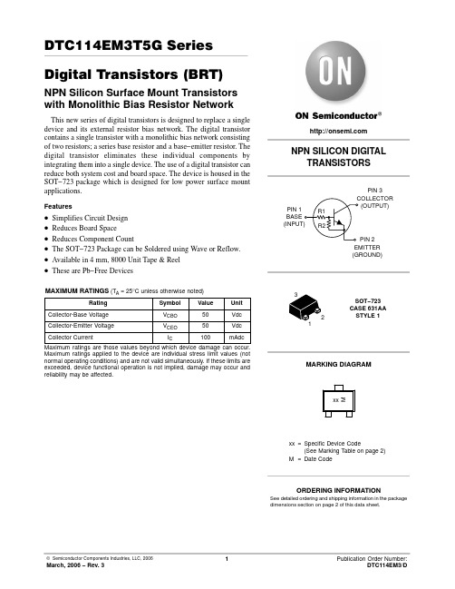
DTC123EM3T5G DTC143EM3T5G
8H 8J
2.2
2.2
SOT−723
4.7
4.7
(Pb−Free)
8000/Tape & Reel
DTC143ZM3T5G*
8K
4.7
47
DTC124XM3T5G*
8L
22
47
DTC123JM3T5G
8M
2.2
47
DTC115EM3T5G
8N
100
Device DTC114EM3T5G
Marking 8A
R1 (K) 10
R2 (K) 10
Package
Shipping†
DTC124EM3T5G
8B
22
22
DTC144EM3T5G
8C
47
47
DTC114YM3T5G
8D
10
47
DTC114TM3T5G
8E
10
∞
DTC143TM3T5G
8F
4.7
DTC114TM3T5G
160
350
−
DTC143TM3T5G
160
350
−
DTC123EM3T5G
8.0
15
−
DTC143EM3T5G
15
30
−
DTC143ZM3T5G
80
200
−
DTC124XM3T5G
80
150
−
DTC123JM3T5G
80
140
−
DTC115EM3T5G
80
150
DTC143TS3中文资料

BCE BCE BCE BCE BCE BCE BCE BCE DAUL DAUL DAUL DAUL DAUL DAUL DAUL DAUL
N+P
SOT-363 (P.29)
MMDT2412 MMDT3904 MMDT2222 MMDT2411 MMDT1036 MMDT1037 MMDT3906 MMDT2907 MMDT2227 MMDT3946
---------------------------------------------------------
FOSAN富信电子 三极管 DTC143Z-产品规格书

安徽富信半导体科技有限公司ANHUI FOSAN SEMICONDUCTOR TECHNOLOGY CO.,LTD.DTC143Z SOT-23Digital Transistor数字晶体管▉Features特点NPN With Bias Resistor Network带偏置电阻▉Absolute Maximum Ratings最大额定值Characteristic特性参数Symbol符号Rat额定值Unit单位Supply Voltage电源电压V CC50V Input Voltage输入电压V IN-5~+30V Output Current输出电流I O100mA Power dissipation耗散功率P C(T a=25℃)200mW Thermal Resistance Junction-Ambient热阻RΘJA625℃/WJunction and Storage TemperatureT J,T stg-55to+150℃结温和储藏温度■Device Marking产品打标DTC143Z=E23ANHUI FOSAN SEMICONDUCTOR TECHNOLOGY CO.,LTD.DTC143Z■ElectricalCharacteristics 电特性(T A =25℃unless otherwise noted 如无特殊说明,温度为25℃)Characteristic 特性参数Symbol 符号Min 最小值Type 典型值Max 最大值Unit 单位Input Voltage 输入电压(V CC =5V ,I O =100µA)V I(off)0.5——VInput Voltage 输入电压(V O =0.3V ,I O =5mA)V I(on)—— 1.3V Output Voltage 输入电压(I O /I I =5mA/0.25mA)V O(on)—0.10.3VInput Current 输入电流(V I =5V)I I —— 1.8mAOutput Current 输出电流(V CC =5V ,V I =0)I O(off)——0.5µADC Current Gain 直流电流增益(V O =5V ,I O =10mA)G I 80——Input Resistor 输入电阻R13.34.7 6.1KΩResistor Ratio 电阻比率R2/R181012Transition frequency 特征频率(V O =10V ,I O =5mA)f T—250—MHzANHUI FOSAN SEMICONDUCTOR TECHNOLOGY CO.,LTD.DTC143Z ■Typical Characteristic Curve典型特性曲线ANHUI FOSAN SEMICONDUCTOR TECHNOLOGY CO.,LTD.DTC143Z■Dimension外形封装尺寸Symbol Dimensions In Millimeters Dimensions In Inches Min Max Min Max A 0.900 1.1500.0350.045A10.0000.1000.0000.004A20.900 1.0500.0350.041b 0.3000.5000.0120.020c 0.0800.1500.0030.006D 2.800 3.0000.1100.118E 1.200 1.4000.0500.055E1 2.2502.5500.0890.100e 0.950TYP0.037TYPe1 1.8002.0000.0710.079L 0.550REF0.022REFL10.3000.5000.0120.020θ0o8o 0o8o。
DTC143ECA中文资料

DTC143ESA
TO-92S
l Any changing of specification will not be informed individua
01-Jun-2002 Rev. A
Page 1 of 2
DTC143EE/DTC143EUA/DTC143EKA DTC143ECA/TC143ESA
Elektronische Bauelemente
NPN Digital Transistors (Built-in Resistors)
Absolute maximum ratings(Ta=25℃)
Parameter Supply voltage Input voltage Output current Power dissipation Junction temperature Storage temperature
Typ Max. 0.5 Unit V V mA µA Conditions VCC=5V ,IO=100µA VO=0.3V ,IO=20 mA IO/II=10mA/0.5mA VI=5V VCC=50V ,VI=0 VO=5V ,IO=10mA 4.7 1 250 6.11 1.2 MHz KΩ
PIN CONNENCTIONS AND MARKING
DTC143EE DTC143EUA
SOT-523
Abbreviated symbol: 23
SOT-323
Abbreviated symbol: 23
DTC143EKA
DTA114ECA DTC143ECA
SOT-23-3L Abbreviated symbol: 23 SOT-23 Abbreviated symbol: 23
DDTC124XUA-7-F;DDTC143XUA-7-F;DDTC114WUA-7-F;DDTC114YUA-7-F;DDTC143FUA-7-F;中文规格书,Datasheet资料

DDTC (R1≠R2 SERIES) UANPN PRE-BIASED SMALL SIGNAL SURFACE MOUNT TRANSISTORFeatures• Ordering Information: See Page 4 • Weight: 0.006 grams (approximate)P/N R1 (NOM) R2 (NOM) Type CodeDDTC113ZUA DDTC123YUA DDTC123JUA DDTC143XUA DDTC143FUA DDTC143ZUA DDTC114YUA DDTC114WUA DDTC124XUA DDTC144VUA DDTC144WUA 1K Ω2.2K Ω2.2K Ω 4.7K Ω4.7K Ω 4.7K Ω 10K Ω10K Ω22K Ω47K Ω47K Ω10K Ω 10K Ω 47K Ω 10K Ω 22K Ω 47K Ω 47K Ω 4.7K Ω 47K Ω 10K Ω 22K Ω N02 N05 N06 N09 N10 N11 N14 N15 N18 N21 N22SOT-323Dim Min Max A 0.25 0.40 B 1.15 1.35 C 2.00 2.20 D0.65 NominalE 0.30 0.40 G1.20 1.40 H 1.802.20 J 0.0 0.10 K 0.90 1.00 L 0.25 0.40 M0.100.18α0° 8° All Dimensions in mmMaximum Ratings @T A = 25°C unless otherwise specifiedCharacteristicSymbol Value Unit Supply Voltage, (3) to (2)V CC50 VInput Voltage, (1) to (2) DDTC113ZUA DDTC123YUA DDTC123JUA DDTC143XUA DDTC143FUA DDTC143ZUA DDTC114YUA DDTC114WUA DDTC124XUA DDTC144VUA DDTC144WUA V IN -5 to +10 -5 to +12 -5 to +12 -7 to +20 -6 to +30 -5 to +30 -6 to +40 -10 to +30 -10 to +40 -15 to +40 -10 to +40 VOutput Current DDTC113ZUA DDTC123YUA DDTC123JUA DDTC143XUA DDTC143FUA DDTC143ZUA DDTC114YUA DDTC114WUA DDTC124XUA DDTC144VUA DDTC144WUA I O 100 100 100 100 100 100 70 100 50 30 30 mAOutput Current AllI C (Max) 100mANotes: 1. No purposefully added lead. 2. Diodes Inc.'s "Green" policy can be found on our website at /products/lead_free/index.php. 3. Product manufactured with Date Code 0627 (week 27, 2006) and newer are built with Green Molding Compound. Product manufactured prior to Date Code 0627 are built with Non-Green Molding Compound and may contain Halogens or Sb2O3 Fire Retardants.R1OUT B CE R2321IN GND(0)132GND (0)C BIN OUTESchematic and Pin Configuration Equivalent Inverter CircuitMaximum Ratings (continued)@T A = 25°C unless otherwise specifiedCharacteristic Symbol Value Unit Output Current All I C (Max) 100 mA Power Dissipation P d200 mW Thermal Resistance, Junction to Ambient Air (Note 4) RθJA625 °C/W Operating and Storage Temperature Range T j, T STG-55 to +150 °CNotes: 4. Mounted on FR4 PC Board with recommended pad layout at /datasheets/ap02001.pdf.Electrical Characteristics@T A = 25°C unless otherwise specifiedCharacteristic Symbol Min Typ Max Unit Test ConditionInput Voltage DDTC113ZUADDTC123YUADDTC123JUADDTC143XUADDTC143FUADDTC143ZUADDTC114YUADDTC114WUADDTC124XUADDTC144VUADDTC144WUAV l(off)0.30.30.50.30.30.50.30.80.41.00.8⎯⎯V CC = 5V, I O = 100μAInput Voltage DDTC113ZUADDTC123YUADDTC123JUADDTC143XUADDTC143FUADDTC143ZUADDTC114YUADDTC114WUADDTC124XUADDTC144VUADDTC144WUAV l(on)⎯⎯3.03.01.12.51.31.31.43.02.55.04.0V V O = 0.3V, I O = 20mAV O = 0.3V, I O = 20mAV O = 0.3V, I O = 5mAV O = 0.3V, I O = 20mAV O = 0.3V, I O = 3mAV O = 0.3V, I O = 5mAV O = 0.3V, I O = 1mAV O = 0.3V, I O = 2mAV O = 0.3V, I O = 2mAV O = 0.3V, I O = 2mAV O = 0.3V, I O = 2mAOutput Voltage V O(on)⎯0.1 0.3 V I O/I l = 5mA/0.25mA DDTC123JUA I O/I l = 5mA/0.25mA DDTC143ZUA I O/I l = 5mA/0.25mA DDTC114YUA I O/I l = 10mA/0.5mA All OthersInput Current DDTC113ZUADDTC123YUADDTC123JUADDTC143XUADDTC143FUADDTC143ZUADDTC114YUADDTC114WUADDTC124XUADDTC144VUADDTC144WUAI l⎯⎯7.23.83.61.81.81.80.880.880.360.160.16mA V I = 5VOutput Current I O(off)⎯⎯0.5 μA V CC = 50V, V I = 0VDC Current Gain DDTC113ZUADDTC123YUADDTC123JUADDTC143XUADDTC143FUADDTC143ZUADDTC114YUADDTC114WUADDTC124XUADDTC144VUADDTC144WUAG l3333803068806824683356⎯⎯⎯V O = 5V, I O = 5mAV O = 5V, I O = 10mAV O = 5V, I O = 10mAV O = 5V, I O = 10mAV O = 5V, I O = 10mAV O = 5V, I O = 10mAV O = 5V, I O = 5mAV O = 5V, I O = 10mAV O = 5V, I O = 5mAV O = 5V, I O = 5mAV O = 5V, I O = 5mAInput Resistor Tolerance ΔR1-30 ⎯+30 % ⎯Resistance Ratio Tolerance ΔR2/R1-20 ⎯+20 % ⎯Gain-Bandwidth Product* f T⎯250 ⎯MHz V CE = 10V, I E = 5mA,f = 100MHz* Transistor - For Reference OnlyTypical Curves – DDTC123JUA-5005010025020015050100T , AMBIENT TEMPERATURE (C)Fig. 1 Derating CurveA °150P , P O W E R D I S S I P A T I O N (m W )D 0.0010.010.111020304050V , C O L L E C T O R E M I T T E R V O L T A G E (V )C E (S A T )I , COLLECTOR CURRENT (mA)Fig. 2 V vs. IC CE(SAT) C101,000100110h , D 100C C U R R E N T G A I NF E I , COLLECTOR CURRENT (mA)Fig. 3 DC Current GainC012342030C , C A P A C IT A N C E (p F )O B V , REVERSE BIAS VOLTAGE (V)Fig. 4 Output CapacitanceR 10515250.0010.01110100012348910I , C O L L E C T O R C U R R E N T (m A )C V , INPUT VOLTAGE (V)Fig. 5 Collector Current vs. Input Voltagein 5670.10.111010203040I , COLLECTOR CURRENT (mA)Fig. 6 Input Voltage vs. Collector CurrentC 50V , I N P U T V O L T A G E (V )i nOrdering Information (Note 3 & 5)Device Packaging Shipping DDTC113ZUA-7-F SOT-323 3000/Tape & ReelDDTC123YUA-7-F SOT-323 3000/Tape & ReelDDTC123JUA-7-F SOT-323 3000/Tape & ReelDDTC143XUA-7-F SOT-323 3000/Tape & ReelDDTC143FUA-7-F SOT-323 3000/Tape & ReelDDTC143ZUA-7-F SOT-323 3000/Tape & ReelDDTC114YUA-7-F SOT-323 3000/Tape & ReelDDTC114WUA-7-F SOT-323 3000/Tape & ReelDDTC124XUA-7-F SOT-323 3000/Tape & ReelDDTC144VUA-7-F SOT-323 3000/Tape & ReelDDTC144WUA-7-F SOT-323 3000/Tape & Reel Notes: 5. For packaging details, go to our website at /datasheets/ap02007.pdf.Marking InformationDate Code Key NXXYMNXX = Product Type Marking CodeSee Page 1 DiagramsYM = Date Code MarkingY = Year ex: T = 2006M = Month ex: 9 = SeptemberYear20022003200420052006200720082009201020112012 Code N P R S T U V W X Y ZMonth Jan Feb Mar Apr May Jun Jul Aug Sep Oct Nov Dec Code 1 2 3 4 5 6 7 8 9 O N DIMPORTANT NOTICEDiodes Incorporated and its subsidiaries reserve the right to make modifications, enhancements, improvements, corrections or other changes without further notice to any product herein. Diodes Incorporated does not assume any liability arising out of the application or use of any product described herein; neither does it convey any license under its patent rights, nor the rights of others. The user of products in such applications shall assume all risks of such use and will agree to hold Diodes Incorporated and all the companies whose products are represented on our website, harmless against all damages.LIFE SUPPORTDiodes Incorporated products are not authorized for use as critical components in life support devices or systems without the expressed written approval of the President of Diodes Incorporated.分销商库存信息:DIODESDDTC124XUA-7-F DDTC143XUA-7-F DDTC114WUA-7-F DDTC114YUA-7-F DDTC143FUA-7-F DDTC143ZUA-7-F DDTC144VUA-7-F DDTC144WUA-7-F DDTC144WUA-7 DDTC144VUA-7DDTC143ZUA-7DDTC123JUA-7 DDTC123JUA-7-F DDTC114WUA-7DDTC113ZUA-7 DDTC113ZUA-7-F DDTC114YUA-7DDTC124XUA-7 DDTC123YUA-7-F DDTC143FUA-7DDTC123YUA-7 DDTC143XUA-7。
DTC143ZUBTL;中文规格书,Datasheet资料
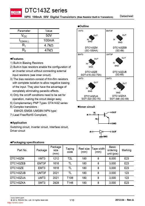
DTC143ZE SOT-416 (SC-75A)
UMT3 OUT IN GND SMT3
DTC143ZUB (SC-85)
OUT IN GND
DTC143ZUA SOT-323 (SC-70)
DTC143ZKA SOT-346 (SC-59)
lInner circuit
lPackaging specifications Part No. DTC143ZM DTC143ZEB DTC143ZE DTC143ZUB DTC143ZUA DTC143ZKA Package VMT3 EMT3F EMT3 UMT3F UMT3 SMT3 Package size (mm) 1212 1616 1616 2021 2021 2928 Taping code T2L TL TL TL T106 T146 Basic Reel size Tape width ordering (mm) (mm) unit (pcs) 180 180 180 180 180 180 8 8 8 8 8 8 8,000 3,000 3,000 3,000 3,000 3,000 Marking E23 E23 E23 123 123 E23
Data Sheet
EMT3F
D
A
x
S A
b e
HE
E
c
e
A2
A
A1
S
l1
b2
Patterm of terminal position areas
MILIMETERS MIN MAX 0.65 0.85 0.00 0.10 0.60 0.80 0.21 0.36 0.08 0.18 1.50 1.70 0.76 0.96 0.50 1.50 1.70 0.37 0.35 0.55 0.10 MILIMETERS MIN MAX 1.05 0.46 0.65 INCHES MIN 0 0.024 0.008 0.003 0.059 0.03 0.02 0.059 0.015 0.014 INCHES MIN MAX 0.041 0.018 0.026 0.022 0.004 0.067 MAX 0.004 0.031 0.014 0.007 0.067 0.038
DDTA143ECA中文资料
2005 S
Jan
Feb March Apr
May Jun
1
2
3
4
5
6
2006 T
2007 U
Jul Aug Sep
7
8
9
2008 V
2009 W
Oct
Nov Dec
O
N
D
DS30333 Rev. 2 - 2
2 of 3
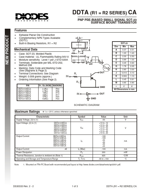
DDTA (R1 = R2 SERIES) CA
NEW PRODUCT
Pd, POWER DISSIPATION (MILLIWATTS)
Output Current
All
Power Dissipation
Thermal Resistance, Junction to Ambient Air (Note 1)
Operating and Storage and Temperature Range
Symbol VCC
VIN
IO
IC (Max) Pd RqJA
J 0.013
K 0.903 1.10
L
0.45 0.61
M
0.85 0.80
a
0°
8°
All Dimensions in mm
SCHEMATIC DIAGRAM
Maximum Ratings @ TA = 25°C unless otherwise specified
Characteristic
hFE, DC CURRENT GAIN (NORMALIZED)
TYPICAL CURVES - DDTA143ECA
250
200
150
100
PDTC143T中文资料

PDTC143T series
VALUE 250 500 500 625 500 500 833
UNIT K/W K/W K/W K/W K/W K/W K/W
MIN. − − − − 200 − 3.3 −
TYP. − − − − − − 4.7 −
MAX. 100 1 50 100 − 100 6.1 2.5
2004 Aug 06
2
Philips Semiconductors
Product specification
NPN resistor-equipped transistors; R1 = 4.7 kΩ, R2 = open
SIMPLIFIED OUTLINE, SYMBOL AND PINNING
ORDERING INFORMATION PACKAGE TYPE NUMBER NAME PDTC143TE PDTC143TEF PDTC143TK PDTC143TM PDTC143TS PDTC143TT PDTC143TU − − − − − − − DESCRIPTION plastic surface mounted package; 3 leads plastic surface mounted package; 3 leads plastic surface mounted package; 3 leads
2004 Aug 06
4
Philips Semiconductors
Product specification
NPN resistor-equipped transistors; R1 = 4.7 kΩ, R2 = open
THERMAL CHARACTERISTICS SYMBOL Rth(j-a) SOT54 SOT23 SOT346 SOT323 SOT490 SOT883 SOT416 Notes 1. Refer to standard mounting conditions. 2. Reflow soldering is the only recommended soldering method. 3. Refer to SOT883 standard mounting conditions; FR4 with 60 µm copper strip line. CHARACTERISTICS Tamb = 25 °C unless otherwise specified. SYMBOL ICBO ICEO IEBO hFE VCEsat R1 Cc PARAMETER collector-base cut-off current collector-emitter cut-off current emitter-base cut-off current DC current gain collector-emitter saturation voltage input resistor collector capacitance IE = ie = 0 A; VCB = 10 V; f = 1 MHz CONDITIONS VCB = 50 V; IE = 0 A VCE = 30 V; IB = 0 A VCE = 30 V; IB = 0 A; Tj = 150 °C VEB = 5 V; IC = 0 A VCE = 5 V; IC = 1 mA IC = 5 mA; IB = 0.25 mA PARAMETER thermal resistance from junction to ambient CONDITIONS in free air note 1 note 1 note 1 note 1 notes 1 and 2 notes 2 and 3 note 1
- 1、下载文档前请自行甄别文档内容的完整性,平台不提供额外的编辑、内容补充、找答案等附加服务。
- 2、"仅部分预览"的文档,不可在线预览部分如存在完整性等问题,可反馈申请退款(可完整预览的文档不适用该条件!)。
- 3、如文档侵犯您的权益,请联系客服反馈,我们会尽快为您处理(人工客服工作时间:9:00-18:30)。
DTC143ZCA
Digital Transistors
Features
x Epitaxial Planar Die Construction
x Complementary NPN Types Available x Built-In Biasing Resistors
Absolute maximum ratings @ 25к
Symbol Parameter Min Typ Max Unit I C Collector current --- 100--- mA V IN Input voltage -5 --- +30
V
P d Power dissipation --- 200--- mW
T j Junction temperature --- 150--- ć
T stg Storage temperature -55--- 150ć
Electrical Characteristics @ 25к
Symbol Parameter Min Typ Max Unit
V I(off) --- --- 1.3 V V I(on)Input voltage (V CC =5V, I O =100A)
(V O =0.3V, I O =5mA)
0.5--- --- V V O(on) Output voltage (I O =5mA,I i =0.25mA) --- --- 0.3 V
I I Input current (V I =5V) --- --- 1.8 mA
I O(off) Output current (V CC =50V, V I =0) --- --- 0.5 A G I DC current gain (V O =5V, I O =10mA)80 --- --- R 1 Input resistance 3.29 4.7 6.11 K ¡
R 2/R 1 Resistance ratio 8 10 12 f T
Transition frequency (V CE =10V, I E =5mA, f=100MHz) --- 250--- MHz omp onents 20736 Marilla Street Chatsworth
! "# $ % ! "#
Revision: A 2011/01/01
1.IN
2.GND
TM
Micro Commercial Components
www.mccsemi .com
1 of 2x Marking :E23
• Lead Free Finish/RoHS Compliant ("P" Suffix designates RoHS Compliant. See ordering information)• Epoxy meets UL 94 V-0 flammability rating • Moisure Sensitivity Level 1tp:///
Revision: A 2011/01/01
Micro Commercial Components
www.mccsemi .com
2 of 2
Ordering Information :
***IMPORTANT NOTICE***
Micro Commercial Components Corp. reserve s the right to make changes without further notice to any product herein to make corrections, modifications , enhancements , improvements , or other changes . Micro Commercial Components Corp . does not assume any liability arising out of the application or use of any product described herein; neither does it convey any license under its patent rights ,nor the rights of others . The user of products in such applications shall assume all risks of such use and will agree to hold Micro Commercial Components Corp . and all the companies whose products are represented on our website, harmless against all damages.
***LIFE SUPPORT***
MCC's products are not authorized for use as critical components in life support devices or systems without the express written
approval of Micro Commercial Components Corporation.
***CUSTOMER AWARENESS***
Counterfeiting of semiconductor parts is a growing problem in the industry. Micro Commercial Components (MCC) is taking strong measures to protect ourselves and our customers from the proliferation of counterfeit parts. MCC strongly encourages customers to purchase MCC parts either directly from MCC or from Authorized MCC Distributors who are listed by country on our web page cited below . Products customers buy either from MCC directly or from Authorized MCC Distributors are genuine parts, have full traceability, meet MCC's quality standards for handling and storage. MCC will not provide any warranty coverage or other assistance for parts bought from Unauthorized Sources. MCC is committed to combat this global problem and encourage our customers to do their part in stopping this practice by buying direct or from authorized distributors.
Device
Packing
Part Number-T P
Tape&Reel;3Kpcs/Reel
/
分销商库存信息: MICRO-COMMERICAL-CO DTC143ZCA-TP。