300SP1J5BLKM7RE;中文规格书,Datasheet资料
SP300;中文规格书,Datasheet资料

PRODUCT DESCRIPTIONFEATURESTYPICAL APPLICATIONS•Precision Instrumentation Systems •Power Supply Monitoring •Test Boxes•Panel-Mount IndicationORDERING INFORMATIONStock Number Standard MeterSP 300LASCAR ELECTRONICS LTD.MODULE HOUSE WHITEPARISHWILTSHIRE SP52SJ UKTEL:+44(1794)884567FAX:+44(1794)884616E-mail:sales@LASCAR ELECTRONICS INC.PO BOX 50727PALO ALTO CA 94303-0727USATEL:+1(650)8389027FAX:+1(650)8335432E-mail:lascarus@LASCAR ELECTRONICS (HK)LIMITED FLAT C,5/FL.,LUCKY FTY.BLDG.63-65HUNG TO ROAD KWUN TONG KOWLOON HONG KONGTEL:+852********FAX:+852********SP 3003½Digit LED Voltmeter ModuleSAFETYT o comply with the Low V oltage Directive (LVD 93/68/EEC),input voltages to the module’s pins must not exceed 60Vdc.The user must ensure that the incorporation of the panel meter into the user’s equipment conforms to the relevant sections of BS EN 61010(Safety Requirements for Electrical Equipment for Measuring,Control and Laboratory Use).ELECTRICAL SPECIFICATIONS••200mV d.c.Full Scale Reading •50mA @+5V d.c.Power Supply •••Bright Red 9.4mm (0.37")Digit Height Programmable Decimal Points LED Display •Display Blanking Facility •Simplified Connection •Splash ProofAuto-zero and Auto-polarity The SP 300features a 200mV d.c.measurement range with auto-zero and auto-polarity.Decimal points are user selectable.The SP 300features a negative rail generator which enables the meter to measure a signal referenced to its own power supply 0V .The bright red LED display ensures excellent readability under low light conditions.It can be blanked in applications requiring low power operation.The module is easily fitted into the panel,using the fixing clip provided.The module's low cost means it will suit high and low volume applications.The design of the panel meter's housing and seal ensures splash proofing in many applications.SpecificationMin.Typ.Max.UnitAccuracy (overall error)*0.1%(±1count)Linearity ±1count Sample rate2.5samples/secOperating temperature range 050°C Warm-up time10minute Temperature stability 150ppm/°C Supply voltage 4.755 5.25V 50mA Input leakage current (Vin =0V)110pA*To ensure maximum accuracy,re-calibrate periodically.Supply currentPO Box 770, Londonderry, NH 03053 1-800-821-0023PIN FUNCTIONS1.V+Positive power supply to the meter.2.0V 0V power supply connection to the meter. Ground for analogue section of A/D converter.It is actively held at 3.05V (nom)below V+and must not be allowed to sink excessive current (>100A)by,for instance,connecting to a higher voltage.4.IH Positive measuring input.5.IL Negative measuring input.6.DP1Connect to 0V to display DP1(199.9).7.DP2Connect to 0V to display DP2(19.99).8.DP3Connect to 0V to display DP3(1.999).A negative supply is generated internally and mirrors the positive supply.For example:if V+is +5V ,then the internally generated V-is -5V .When measuring with the input referenced to the same supply rail as that of the panel meter,then the limitations on the input range are (V-+1.5V)to (V+-1.5V).LCOM Normally Open.Connects IL to COM.µNote:Solder Links:14532691678分销商库存信息: MARTEL-ELECTRONICS SP300。
SD387EVKNOPB;中文规格书,Datasheet资料
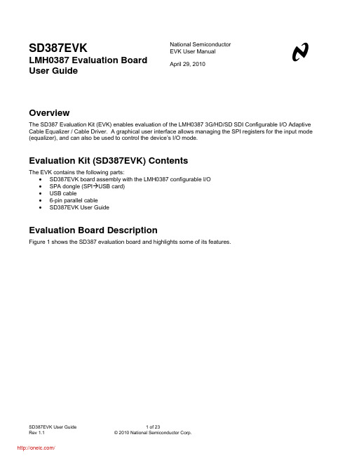
SD387EVKLMH0387 Evaluation Board User Guide National Semiconductor EVK User ManualApril 29, 2010OverviewThe SD387 Evaluation Kit (EVK) enables evaluation of the LMH0387 3G/HD/SD SDI Configurable I/O Adaptive Cable Equalizer / Cable Driver. A graphical user interface allows managing the SPI registers for the input mode (equalizer), and can also be used to control the device’s I/O mode.Evaluation Kit (SD387EVK) ContentsThe EVK contains the following parts:•SD387EVK board assembly with the LMH0387 configurable I/O•SPA dongle (SPIÆUSB card)• USB cable•6-pin parallel cable• SD387EVK User GuideEvaluation Board DescriptionFigure 1 shows the SD387 evaluation board and highlights some of its features.FIGURE 1. SD387 Evaluation BoardInputs and Outputs: BNC_IO Input/Output, SDI Input, and SDO OutputThe bidirectional I/O (J1) is a 75Ω BNC connector. When the LMH0387 is configured as an input, the input signal on the BNC_IO pin should conform to the SMPTE 424M, SMPTE 292M, or SMPTE 259M standards. When the LMH0387 is configured as an output, the BNC_IO pin will drive SMPTE SDI signal levels (800 mV P-P into 75Ω).The SDI input connectors (J2 and J3) are 50Ω SMA connectors. This cable driver input includes a 100Ω differential termination resistor (R5) at the LMH0387 device and is optimized for 100Ω differential input.The SDO output connectors (J4 and J5) are 50Ω SMA connectors. When using only one side of this equalizer output pair, the other side should be terminated with a 50Ω SMA termination. For example, when only using theSDO output, SDO¯¯¯¯ should be terminated with a 50Ω SMA termination.DC Power ConnectorsThe VCC and GND power connectors should be powered with a DC input voltage of 3.3V ± 5% (3.6V maximum).JP2 ControlsCD ¯¯¯JP2 allows monitoring of the Carrier Detect (CD¯¯¯ ) at the BNC_IO pin while in the input mode (equalizer). CD ¯¯¯ is asserted low when an input signal is detected at the BNC_IO pin, and high when no input signal is present. TX_ENJP2 allows control of the TX_EN pin to enable or disable the cable driver. The LMH0387 TX_EN pin has aninternal pullup to enable the cable driver by default, so this pin may be left unconnected when using the LMH0387 in the output mode. To disable the cable driver, place a jumper to tie TX_EN to GND. When using the LMH0387 in the input mode, the cable driver must be disabled by tying TX_EN low. TX_EN may optionally be controlled via the GUI using the SPA dongle as described below. SD/HD¯¯¯ JP2 allows control of the SD/HD¯¯¯ pin for setting the slew rate for the BNC_IO pin while the LMH0387 is in the output mode (cable driver). This pin may be connected to GND for the faster HD/3G slew rate or connected to V CC for theslower SD slew rate. The LMH0387 SD/HD¯¯¯ pin has an internal pulldown to enable the HD/3G slew rate by default.SPI Header (JP1)JP1 is the SPI (Serial Peripheral Interface) header. It allows access to the SPI pins (SS ¯¯¯ , MISO, MOSI, and SCK) to control the SPI registers of the LMH0387 equalizer. To use the SPI interactive GUI, plug the 6-pin parallel cable between this header and JP7 on the SPA dongle to connect the pins one-for-one as shown in Table 1. The SPA dongle requires special software and must be connected to the PC via the USB – see the Software Setup section.TABLE 1. SPI Connections between SD387 and SPA DongleSD387 JP1 SPA Dongle JP7 Pin # Name Pin # Name1 GND Æ 1 GND2 SCK Æ 2 MCK3 MOSI Æ 3 MOSI4 MISO Æ 4 MOSI5 SS Æ 5 SS6 GND Æ 6 GNDCarrier Detect LED (D1)D1 shows the status of Carrier Detect at the LMH0387 equalizer input. This LED is GREEN when an input signal has been detected at the BNC_IO pin, and OFF when no input is detected.SPA Dongle DescriptionThe SPA dongle is required to use the SPI interactive GUI. The SPA dongle connects between the LMH0387 SPI pins and the USB input of a PC. The SPA dongle is shown in Figure 2. JP7 is the SPI Header. The SPA dongle is powered through the USB, and the D1 LED is RED when the SPA dongle is connected to a PC via the USB to indicate the board is powered.FIGURE 2. SPA DongleFigure 3 shows the connection between the SD387 and the SPA dongle. For proper operation, the SPI pins must be connected between the SD387 JP1 and the SPA dongle JP7. Optionally, a single wire may be connected between the SD387 TX_EN pin (JP2) and the SPA dongle PA0 (J7) to enable software control of the LMH0387 cable driver enable functionality, and allow the GUI to fully control the LMH0387 I/O Mode as described on page 8. If this connection is not used, then the TX_EN can be controlled manually with a jumper.FIGURE 3. SD387 Connection to SPA DongleSoftware SetupSystem RequirementsOperating System:Windows XP or VistaUSB: 2.0InstallationDownload the latest software from the LMH0387 Evaluation Board page. Extract the ALPF_monthdayyear_major version_minor version.exe” (ex. ALPF_04062010_128_0002.exe) file to a temporary location that can be deleted later.Make sure the SPA dongle is not connected to the PC. The following installation instructions are for the Windows XP Operating System.Install the ALP softwareExecute the ALP Setup Wizard program called “ALPF_monthdayyear_major version_minor version.exe” (ex. ALPF_04062010_128_0002.exe) that was extracted to a temporary location.There are 7 steps to the installation once the setup wizard is started:1. Select the “Next” button.2. Select “I accept the agreement” and then select the “Next” button.3. Select the location to install the ALP software and then select the “Next” button.4. Select the location for the start menu shortcut and then select the “Next” button.5. There will then be a screen that allows the creation of a desktop and Quick Launch icon. After selectingthe desired choices select the “Next” button.6. Select the “Install” button, and the software will then be installed to the selected location.7. Uncheck “Launch Analog LaunchPAD” and select the “Finish” button. The ALP software will start if“Launch Analog LaunchPAD” is checked, but it will not be useful until the USB driver is installed.Connect JP1 of the SD387 evaluation board to JP7 of the SPA dongle via the 6-pin parallel cable as shown in Table 1. Power on the SD387 evaluation board with a 3.3 VDC power supply. Connect the SPA dongle to the PC with the USB cable. The “Found New Hardware Wizard” will open on the PC. Proceed to the next section to install the USB driver.Install the USB driverThere are 6 steps to install the USB driver:1. Select “No, not at this time” then select the “Next” button.2. Select “Install from a list or specific location” then select the “Next” button.3. Select “Search for the best driver in these locations”. Uncheck “Search removable media” and check“Include this location in the search”.4. Browse to the Install Directory which is typically located at “C:\Program Files\National SemiconductorCorp\Analog LaunchPAD\vx.x.x\Drivers” and select the “Next” button. Windows should find the driver.5. Select “Continue Anyway”.6. Select the “Finish” button.The software installation is complete. The ALP software may now be launched, as described in the next section.Software DescriptionStartupMake sure all the software has been installed and the hardware is powered on and connected to the PC. Execute “Analog LaunchPAD” from the start menu. The default start menu location is “Programs\National Semiconductor Corp\Analog LaunchPAD vx.x.x\Analog LaunchPAD”.The application should come up in the state shown in Figure 4 below. If it does not, see “Trouble Shooting” at the end of this document. Click on “LMH0387 – Nano” to select the device and open up the device profile and its associated tabs.FIGURE 4. ALP Startup Screen for the LMH0387Information TabThe Information tab is shown in Figure 5.FIGURE 5. LMH0387 Information TabFunctional TabThe Functional tab is the main tab of the GUI and presents a high level view of the LMH0387 equalizer, as shownin Figure 6.I/O Mode Controlprovided an additional wire is connected between the SD387 TX_EN and theSPA dongle PA0, as shown in Figure 3. The connection between TX_EN andPA0 allows software control of the LMH0387 cable driver enable functionality.If the SD387 TX_EN is not connected to the SPA dongle PA0, then TX_ENmay be controlled manually with a jumper and the I/O Mode Control will have no effect on the LMH0387 cable driver.The default LMH0387 I/O Mode setting is the Input (Rx) Mode, or equalizer mode. This default setting allows full control of the LMH0387 equalizer. The three I/O modes are described below.Input (Rx) Mode: Configures the LMH0387 for the input mode (equalizer enabled and cable driver disabled). This is the default setting. The LMH0387 equalizer is set to auto sleep, and if TX_EN is connected to PA0, then PA0 will drive TX_EN low to disable the LMH0387 cable driver. If this TX_EN Æ PA0 connection is not made, then the LMH0387 cable driver should be manually disabled by setting a jumper to tie TX_EN to GND.Output (Tx) Mode: Configures the LMH0387 for the output mode (cable driver enabled and equalizer disabled). The LMH0387 equalizer is forced to sleep. If TX_EN is connected to PA0, then PA0 will drive TX_EN high to enable the LMH0387 cable driver. If this TX_EN Æ PA0 connection is not made, then the LMH0387 cable drivershould be manually enabled by pulling the jumper between TX_EN and GND (TX_EN should be open).Tx Loopback Mode: Configures the LMH0387 for the output mode with a loopback path (cable driver andequalizer both enabled). The LMH0387 equalizer is set to auto sleep. If TX_EN is connected to PA0, then PA0 will drive TX_EN high to enable the LMH0387 cable driver. If this TX_EN Æ PA0 connection is not made, then theLMH0387 cable driver should be manually enabled by pulling the jumper between TX_EN and GND (TX_EN should be open). In this mode, the cable driver output on the BNC_IO pin is looped back to the LMH0387 equalizeroutputs (SDO and SDO¯¯¯¯ ), so the cable driver output may be observed both at BNC_IO pin and at the SDO/SDO ¯¯¯¯ output pins.The Cable Driver TX_EN indicator shows the current status of the TX_EN control (only if TX_EN is connected to PA0). It is GREEN to indicate TX_EN is driven high and the LMH0387 cable driver is enabled, or OFF to indicate TX_EN is driven low and the LMH0387 cable driver is disabled.Equalizer Sleep Mode and Carrier DetectThe Equalizer Sleep Mode control shows the status of the Sleep Mode register bits and allows control over the sleep mode. The Equalizer Sleep Mode settings are as follows:On: Force the equalizer into sleep mode (powered down) regardless of whether there is an input signal or not.Off: Disable sleep mode (force equalizer to stay enabled).Auto: Sleep mode active when no input signal detected (default mode).The Equalizer Sleep Status indicator shows the current sleep status of the equalizer. It is GREEN to indicate sleeping or OFF to indicate not sleeping.The Carrier Detect shows the status of the BNC_IO input carrier detect. It is GREEN to indicate the input signal is present or OFF to indicate the input signal is absent.Equalizer Output SwingThe Equalizer Output Swing control shows the current value of the LMH0387 equalizer output amplitude and allows adjustment in 100 mV increments from 400 mV P-P to 800 mV P-P . The default setting is 700 mV P-P . The Equalizer Output Swing may be set either by clicking on the “+” or “-” buttons, or by grabbing and spinning the “handle” on the knob for a quick adjustment.Equalizer Output OffsetThe Equalizer Output Offset control shows the current value of the LMH0387 equalizeroutput common mode voltage and allows adjustment in 200 mV increments from 1.05Vto 1.85V. At the “Max” setting, the outputs are referenced to the positive supply and theoutput common mode is 2.1V. The default setting is 1.25V. The Equalizer Output Offsetmay be set either by clicking on the “+” or “-”buttons, or by grabbing and spinning the“handle” on the knob for a quick adjustment.Equalizer Output MuteThe Equalizer Output Mute indicator shows the mute status, and the button may be used totoggle the mute function. The indicator is GREEN to indicate mute (equalizer outputs aremuted) and OFF to indicate normal mode (outputs are not muted).Extended 3G Reach ModeThe Extended 3G Reach Mode indicator shows the status of the Extended 3G ReachMode register bit, and the button may be used to toggle this register bit. The indicator isGREEN when the bit is set for extended 3G reach mode, and OFF when the equalizer isset for normal mode. Note that the indicator shows the status of the register bit – notwhether the device is actually in extended 3G reach mode or not. If extended 3G reachmode is set, the equalizer will remain in this mode until the input cable is physically changed or power is cycled. For example, extended 3G reach mode is forced, and then it is turned off. The indicator will show it is off, but the equalizer will still be in extended 3G reach mode until the input cable is changed or the device power is cycled. The GUI provides a simple way to reset the extended 3G reach mode: the Extended 3G Reach Mode Reset button. This button toggles the equalizer sleep mode, and has a similar effect to removing and re-applying the input cable.分销商库存信息: NATIONAL-SEMICONDUCTOR SD387EVK/NOPB。
ADS1278EVM-PDK;ADS1278EVM;中文规格书,Datasheet资料
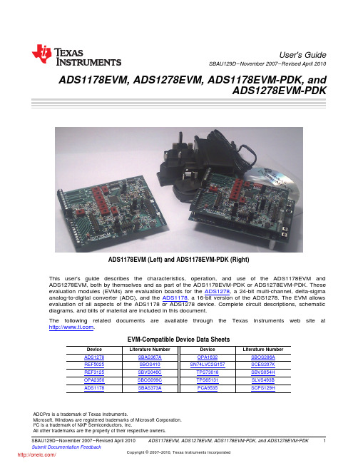
User's GuideSBAU129D–November2007–Revised April2010 ADS1178EVM,ADS1278EVM,ADS1178EVM-PDK,andADS1278EVM-PDKADS1178EVM(Left)and ADS1178EVM-PDK(Right)This user's guide describes the characteristics,operation,and use of the ADS1178EVM and ADS1278EVM,both by themselves and as part of the ADS1178EVM-PDK or ADS1278EVM-PDK.These evaluation modules(EVMs)are evaluation boards for the ADS1278,a24-bit multi-channel,delta-sigma analog-to-digital converter(ADC),and the ADS1178,a16-bit version of the ADS1278.The EVM allows evaluation of all aspects of the ADS1178or plete circuit descriptions,schematic diagrams,and bills of material are included in this document.The following related documents are available through the Texas Instruments web site at .EVM-Compatible Device Data SheetsADCPro is a trademark of Texas Instruments.Microsoft,Windows are registered trademarks of Microsoft Corporation.I2C is a trademark of NXP Semiconductors,Inc.All other trademarks are the property of their respective owners.1 SBAU129D–November2007–Revised April2010ADS1178EVM,ADS1278EVM,ADS1178EVM-PDK,and ADS1278EVM-PDK Submit Documentation FeedbackContents1EVM Overview (4)2Analog Interface (4)3Digital Interface (5)4Power Supplies (7)5Voltage Reference (8)6Power-Down,Mode,and Format Control (8)7Clock Source (9)8EVM Operation (9)9ADS1278EVM-PDK Kit Operation (13)10Evaluating Performance with the ADCPro Software (26)11Schematics and Layout (31)List of Figures1Connector J2 (6)2Connectors J15,J16 (7)3Connector J1 (8)4Switch S1 (8)5Jumper J19 (9)6Amplifier Selection Switches (10)7ADS1278EVM Default Jumper Locations (12)8MMB0Initial Setup (14)9Connecting ADS1278EVM to MMB0 (15)10Connecting an AC Adapter (16)11Laboratory Power-Supply Connection (17)12NI-VISA Driver Installation (18)13NI-VISA Driver Installation Question (19)14NI-VISA Driver Installing (19)15NI-VISA Driver Complete Installation (20)16NI-VISA Driver Verification Using Device Manager (20)17ADCPro Software Start-up Display Window (21)18ADS1278EVM-PDK Plug-In Display Window (22)19Install New Driver Wizard Screen1 (23)20Install New Driver Wizard Screen2 (23)21Install New Driver Wizard Screen3 (24)22Install New Driver Wizard Screen4 (24)23Install New Driver Wizard Screen5 (25)24USBStyx Driver Verification Using Device Manager (25)25Channel Enable (26)26Manual Channel Control (27)27Clock Settings and Mode (28)28Operating Mode (29)29Output Data Format (29)30Progress Bar While Collecting Data (30)List of Tables1J9/J7:Analog Interface Pinout (5)2J8:Supplemental Analog Interface Pinout (5)3J5:Serial Interface Pins (6)4J3Configuration:Power-Supply Input (7)2ADS1178EVM,ADS1278EVM,ADS1178EVM-PDK,and ADS1278EVM-PDK SBAU129D–November2007–Revised April2010Submit Documentation Feedback5J15+10V Selection (7)6J16–10V Selection (7)7List of Switches (12)8Operating Modes:Clock Frequency (27)9ADS1278EVM Bill of Materials (31)3 SBAU129D–November2007–Revised April2010ADS1178EVM,ADS1278EVM,ADS1178EVM-PDK,and ADS1278EVM-PDK Submit Documentation FeedbackEVM Overview 1EVM Overview1.1FeaturesADS1178EVM/ADS1278EVM Features:•Contains all support circuitry needed for the ADS1178/ADS1278•+10V and–10V generated from the+5V supply or supplied externally•Voltage reference options:external or onboard•Clock options:External clock source or27MHz onboard crystal oscillator•GPIO access•Compatible with the TI Modular EVM SystemADS1178EVM-PDK/ADS1278EVM-PDK Features:•Easy-to-use evaluation software for Microsoft®Windows®XP•Data collection to text files•Built-in analysis tools including scope,FFT,and histogram displays•Complete control of board settings•Easily expandable with new analysis plug-in tools from Texas InstrumentsFor use with a computer,the ADS1178EVM-PDK or ADS1278EVM-PDK is available.This kit combines the ADS1178EVM/ADS1278EVM board with the DSP-based MMB0motherboard,and includes ADCPro™software for evaluation.The MMB0motherboard allows the ADS1178EVM/ADS1278EVM to be connected to the computer via an available USB port.This manual shows how to use the MMB0as part of theADS1178EVM-PDK/ADS1278EVM-PDK,but does not provide technical details about the MMB0itself.ADCPro is a program for collecting,recording,and analyzing data from ADC evaluation boards.It is based on a number of plug-in programs,so it can be expanded easily with new test and data collection plug-ins.The ADS1178EVM-PDK/ADS1278EVM-PDK is controlled by a plug-in running in ADCPro.For moreinformation about ADCPro,see the ADCPro™Analog-to-Digital Converter Evaluation Software User'sGuide(/lit/ug/sbau128/sbau128.pdf),available for download for the TI web site.This manual covers the operation of both the ADS1178EVM/ADS1278EVM and theADS1178EVM-PDK/ADS1278EVM-PDK.Throughout this document,the abbreviation EVM and the term evaluation module are synonymous with the ADS1178EVM/ADS1278EVM.For clarity of reading,thismanual will refer only to the ADS1278EVM or ADS1278EVM-PDK,but operation of the EVM and kit for the ADS1178is identical,unless otherwise noted.1.2IntroductionThe ADS1278EVM is an evaluation module built to the TI Modular EVM System specification.It can be connected to any modular EVM system interface card.The ADS1278EVM is available as a stand-alone printed circuit board(PCB)or as part of theADS1278EVM-PDK,which includes an MMB0motherboard and software.As a stand-alone PCB,theADS1278EVM is useful for prototyping designs and firmware.Note that the ADS1278EVM has no microprocessor and cannot run software.To connect it to a computer, some type of interface is required.2Analog InterfaceFor maximum flexibility,the ADS1278EVM is designed for easy interfacing to multiple analog sources.Samtec part numbers SSW-110-22-F-D-VS-K and TSM-110-01-T-DV-P provide a convenient10-pin,dual-row,header/socket combination at J9.This header/socket provides access to the analog input pins of the ADS1278.Consult Samtec at or call1-800-SAMTEC-9for a variety of mating connector options.These signals can also be connected to the terminal block J7.In addition to J9(and J7),terminal block J8also provides additional analog inputs to accommodate the large number of input channels available on the ADS1278.4ADS1178EVM,ADS1278EVM,ADS1178EVM-PDK,and ADS1278EVM-PDK SBAU129D–November2007–Revised April2010Submit Documentation Feedback Digital Interface Most of the pins on J7,J8and J9are directly connected,with no filtering or e appropriate caution when handling these pins.Table1and Table2summarize the pinouts for analog interfaces J9/J7 and J8,respectively.Table1.J9/J7:Analog Interface PinoutPin Number Signal DescriptionJ9.1,J7-2A1N AINN1,ADS1278J9.2,J7-3A1P AINP1,ADS1278J9.3,J7-4A2N AINN2,ADS1278J9.4,J7-5A2P AINP2,ADS1278J9.5,J7-6A3N AINN3,ADS1278J9.6,J7-7A3P AINP3,ADS1278J9.7,J7-8A4N AINN4,ADS1278J9.8,J7-9A4P AINP4,ADS1278J9.18EXTREFN External Reference source input(–side ofdifferential input)J9.20EXTREFP External Reference source input(+side ofdifferential input)J9.10-16(even)Unused—J9.15Unused—J9.9-19(odd),J7-1AGND Analog ground connections(except J1.15)Table2.J8:Supplemental Analog Interface PinoutPin Number Signal DescriptionJ8.1GND Analog groundJ8.2A5N AIN5N,ADS1278J8.3A5P AIN5P,ADS1278J8.4A6N AIN6N,ADS1278J8.5A6P AIN6P,ADS1278J8.6A7N AIN7N,ADS1278J8.7A7P AIN7P,ADS1278J8.8A8N AIN8N,ADS1278J8.9A8P AIN8P,ADS12783Digital Interface3.1Serial Data InterfaceThe ADS1278EVM is designed to easily interface with multiple control platforms.Samtec part numbers SSW-110-22-F-D-VS-K and TSM-110-01-T-DV-P provide a convenient10-pin,dual-row,header/socket combination at J5.This header/socket provides access to the digital control and serial data pins of theADC.Consult Samtec at or call1-800-SAMTEC-9for a variety of matingconnector options.5 SBAU129D–November2007–Revised April2010ADS1178EVM,ADS1278EVM,ADS1178EVM-PDK,and ADS1278EVM-PDK Submit Documentation FeedbackDigital Interface All logic levels on J5are3.3V CMOS,except for the I2C™pins.These pins conform to3.3V I2C rules.Table3describes the J5serial interface pins.Table3.J5:Serial Interface PinsPin No.Pin Name Signal Name I/O Type Pullup FunctionJ5.1CNTL SYNC In High—J5.2GPIO0MODE0In High—J5.3CLKX SCLK In None ADS1278SPI clock J5.4DGND DGND In/Out None Digital groundJ5.5CLKR CLKR Out None SCLK clockJ5.6GPIO1MODE1In High—J5.7FSX DRDY/FSYNC In/Out Low—J5.8GPIO2FORMAT0In High—J5.9FSR DRDY/FSYNC In/Out None—J5.10DGND DGND In/Out None Digital groundJ5.11DX DIN In None ADS1278SPI datain J5.12GPIO3FORMAT1In High—J5.13DR DOUT1Out None ADS1278data out J5.14GPIO4FORMAT2In None—J5.15/INT DRDY/FSYNC Out None—J5.16SCL SCL I2C N/A I2C clockJ5.17TOUT CLK In None Can be used toprovide a clock froma processorJ5.18DGND DGND In/Out None Digital groundJ5.19GPIO5CLK Select—None—J5.20SDA SDA I2C N/A I2C dataMany pins on J5have weak pull-up/down resistors.These resistors provide default settings for many of the control pins.Many pins on J5correspond directly to ADS1278pins.See the ADS1278product data sheet for complete details on these pins.3.2Data OutputMost data communications are directed through DOUT1.The data from all eight channels can beobserved on the DOUT1pin using the TDM mode.That is the signal that is used by theADS1278EVM-PDK to read back and display all the channels.All the data output signals(DOUT1toDOUT8)can be monitored on J2.Figure1illustrates the pinout for J2.Figure1.Connector J26ADS1178EVM,ADS1278EVM,ADS1178EVM-PDK,and ADS1278EVM-PDK SBAU129D–November2007–Revised April2010Submit Documentation Feedback Power Supplies 4Power SuppliesJ3is the power-supply input connector.Table4lists the configuration details for J3.Analog inputs to the ADC can be applied directly to the device(see Section8.1,Analog Input),bypassing the onboardamplifiers,and in this case only+5V and+3.3V are required to power the EVM.If the amplifiers are used, an additional bipolar supply is needed to power them.The EVM includes a switching power supply togenerate a+10V and–10V supply.For optimum noise performance,the external supplies(+VA and–VA) should be used.Table4.J3Configuration:Power-Supply InputPin No.Pin Name Function RequiredJ3.1+VA+10V to+15V Yes,unless onboard+10V isused.J3.2–VA-10V to–15V Yes,unless onboard–10V isused.J3.3+5VA+5V analog supply AlwaysJ3.4–5VA–5V analog supply NoJ3.5DGND Digital ground input YesJ3.6AGND Analog ground input YesJ3.7+1.8VD 1.8V digital supply NoJ3.8VD1Not used NoJ3.9+3.3VD 3.3V digital supply AlwaysJ3.10+5VD+5V Used to generate+10V/–10V The1.8V for DVDD comes from the voltage regulator U16using3.3V as the source voltage input.All of the power supplies AVDD(+5V),DVDD(1.8V),and IOVDD(3.3V)have corresponding jumpers J10, J11(AVDD),J13(DVDD)and J14(IOVDD)that can be replaced with a current meter to measure therespective supply currents.4.1Bipolar Power OptionsJ15and J16require a jumper to select the voltage used by the onboard amplifiers.The external voltages can range from10V to15V.The onboard voltage is always10V.Table5and Table6list the options for J15and J16,respectively.Figure2shows the pinout for connectors J15and J16.Table5.J15+10V SelectionJumper Name Function1-2(OB)+10V Select the+10V that is generatedon the EVM2-3(EXT)+VA Select the external+VA voltageTable6.J16–10V SelectionJumper Name Function1-2–10V Select the–10V that is generatedon the EVM2-3–VA Select the external–VA voltageFigure2.Connectors J15,J167 SBAU129D–November2007–Revised April2010ADS1178EVM,ADS1278EVM,ADS1178EVM-PDK,and ADS1278EVM-PDK Submit Documentation FeedbackVoltage Reference 5Voltage ReferenceThe ADS1278EVM has three sources for the reference voltage.Jumper J1can select the voltage from either the REF3125(U1)or REF5025(U2).The reference from either source is filtered and buffered by U3A.Switch S1chooses either the onboard reference or the external reference voltage that is connected to the reference pins of J9.Figure3illustrates the pinout for connector J1.Figure4shows switch S1as it appears on the EVM.Figure3.Connector J1Figure4.Switch S16Power-Down,Mode,and Format ControlThe ADS1278has several pins to control the power-down of individual channels,and mode and format for the digital interface.These pins are controlled on the EVM either through software or hardware(usingswitches S10and S11).For users of the ADS1278EVM as a stand-alone module,these pins may be pulled high or low through DIP switches S10and S11.Refer to the ADS1278product data sheet for complete details on these pins and which state sets which options.For use in the ADS1278EVM-PDK,the state of these pins is controlled by software,using the I2C portexpander on the EVM.When used in the ADS1278EVM-PDK,the DIP switches S10and S11must all be switched so that they are down,toward the center of the board.The ADS1278EVM-PDK software willcheck at startup to verify that these switches are set correctly,and will generate an error message if they are not.However,it cannot detect if the switches are changed after startup.CAUTIONWhen using the EVM as part of the ADS1278EVM-PDK,the DIP switches S10and S11must all be switched so that they are down,toward the center of theboard.Failure to do so may damage the EVM.8ADS1178EVM,ADS1278EVM,ADS1178EVM-PDK,and ADS1278EVM-PDK SBAU129D–November2007–Revised April2010Submit Documentation Feedback Clock Source 7Clock SourceThe ADS1278clock can come from one of several sources:the onboard27MHz crystal oscillator,a clock supplied by a processor on the TOUT pin(J5.17),or an external clock source connected to J18.1(ground) and J18.2(signal).If the onboard27MHz oscillator is selected,the device can be run in the high-speed mode,thehigh-resolution mode,the low-power mode,or low-speed modes with CLKDIV set to1.If the performance of the device must be explored with CLKDIV set to0in the low-power and low-speed modes,an external clock must be provided to the board,either using the TOUT connection or having an external clock source connected to J18.The same condition is true if frequencies other than the27MHz provided by theonboard oscillator must be investigated.7.1Usage in PDKIf using the ADS1278EVM as part of the ADS1278EVM-PDK,J19should not have any pins shorted.Remove any shorting blocks on jumper J19.The ADS1278EVM-PDK software will allow selection of the clock source under software control(this is accomplished by using port05of the I2C expander U17).The software allows selection of the onboard27MHz oscillator,or a clock provided by a PLL on the MMB0that directly drives the appropriate CLK pins of the interface,or an external,customer-supplied clock.If anexternal clock is selected with the software,this clock must be provided on J18.Note that if the external clock is selected and no clock is provided,the software may hang waiting for data from the converter.7.2Usage as a Stand-Alone EVMIf using the EVM in your own system and not with the PDK hardware and software,observe the following recommendations:•J17should be removed if the external clock source is used and the TOUT pin is still driven by a processor in order to avoid conflicts.•Jumper J19can be used to always select the27MHz crystal(IOVDD position)or allow the onboard/external clock selection to be controlled by GPIO5(J5.19),as shown in Figure5.Figure5.Jumper J198EVM OperationThe following section provides information on the analog input,digital control,and general operatingconditions of the ADS1278EVM.8.1Analog InputFour of the analog input sources(channels1–4)can be applied directly to J9(top or bottom side)orthrough signal-conditioning modules available for the modular EVM system.Terminal block J7isconnected in parallel with the analog signal connections to J9.The additional four channel sources(5-8) can be applied to the terminal block J8.Each input signal can be selected to connect directly to the analog inputs of the ADS1278or they can use the OPA1632buffers that are provided.Switches S2–9can be switched away from the ADS1278to select the Terminal Block(TBK)or towards the ADS1278to select the Amplifier(AMP)for the analog inputs1 through8,as shown in Figure6.9 SBAU129D–November2007–Revised April2010ADS1178EVM,ADS1278EVM,ADS1178EVM-PDK,and ADS1278EVM-PDK Submit Documentation FeedbackEVM Operation Figure6.Amplifier Selection Switches8.2Digital ControlThe digital control signals can be applied directly to J5(top or bottom side).The modular ADS1278EVM can also be connected directly to a DSP or microcontroller interface board,such as the5-6K Interface or HPA-MCUInterface boards available from Texas Instruments,or the MMB0if purchased as part of theADS1278EVM-PDK.For a list of compatible interface and/or accessory boards for the EVM or theADS1278,see the relevant product folder on the TI web site.Some of the digital signals are controlled directly with pins on J5.Other signals such as the Power Down controls can only be controlled with slide switches or by U17and U18that are set up and read using the I2C signals on pins16and18of J5.The Format and Mode pins can be controlled by all three methods(slide switches,GPIO pins on J5,and the I2C control from U17).10ADS1178EVM,ADS1278EVM,ADS1178EVM-PDK,and ADS1278EVM-PDK SBAU129D–November2007–Revised April2010Submit Documentation Feedback分销商库存信息:TIADS1278EVM-PDK ADS1278EVM。
SPU0410HR5H-PB, 规格书,Datasheet 资料
“Ultra‐Mini” SiSonic™ Microphone Specification With MaxRF Protection –Halogen FreeKnowles Acoustics1151 Maplewood DriveItasca, IL 601431. DESCRIPTION AND APPLICATION1.1 Description“Ultra Mini” Surface Mount Silicon Microphone with Maximum RF Protection –Halogen Free 1.2 ApplicationHand held consumer electronics2. PART MARKINGIdentification Number ConventionS 1 2 34 5 6 7S: Manufacturing Location“S” –Knowles Electronics SuzhouSuzhou, China“No Alpha Character” –Knowles Electronics ItascaItasca, IL USA 3“E” –Engineering Samples Digits 1 –7: Job Identification Number3.TEMPERATURE RANGE 3.1 Operating Temperature Range: ‐40°C to +100°C 3.2 Storage Temperature Range: ‐40°C to +100°C4. ACOUSTIC & ELECTRICAL SPECIFICATIONSSymbol ConditionLimitsUnit Min.Nom.Max.Directivity Omni‐directionalSensitivity S@ 1kHz (0dB=1V/Pa)‐45‐42‐39dB Output impedance Z OUT@ 1kHz (0dB=1V/Pa)‐‐‐‐‐‐300ΩCurrent Consumption I DSS across 1.5 to 3.6 volts‐‐‐‐‐‐250μA Signal to Noise Ratio S/N@ 1kHz (0dB=1V/Pa)‐‐‐59‐‐‐dB Supply Voltage Vs 1.5‐‐‐ 3.6VSensitivity Loss acrossVoltage Change in sensitivity over3.6v to 1.5vNo Change Across VoltageRangedBTHD At 100dB SPL, THD < 1%At 115dB SPL, THD < 10%dB5. FREQUENCY RESPONSE CURVE66. MECHANICAL SPECIFICATIONS7. RECOMMENDED CUSTOMER7LAND PATTERN8. RECOMMENDED SOLDER STENCIL PATTERNN/A9. RECOMMENDED INTERFACE CIRCUIT10. DETAIL 10PACKAGING11. SOLDER REFLOW PROFILE170–180°CSolder Melt Pre ‐heat 260°C230°Csec sec Stage Temperature ProfileTime (maximum)Pre ‐heat 170 ~ 180 C 120 sec.Solder Melt Above 230 C 100 sec.100 sec.120 sec.Notes:1.Do not pull a vacuum over the port hole of the microphone. Pulling avacuum over the port hole can damage the device.the reflow process.Board washing and cleaning Peak260 C maximum30 sec.2.Do not board wash afteragents can damage the device. Do not expose to ultrasonic processing or cleaning.3.Number of Reflow = recommend no more than 3 cycles.12ADDITIONAL NOTES (A)Shelf life: Twelve (12) months when devices are to be stored in factory supplied, unopened ESD moisture sensitive bag under maximum environmental conditions of 30ºC, 70% R.H. (B)MSL (moisture sensitivity level) Class 2a.12.13. RELIABILITY SPECIFICATIONSNote: After test conditions are performed, the sensitivity of the microphone shall not deviate more than 3dB from its initial value.Test DescriptionThermal Shock100 cycles of air‐air thermal shock from ‐40C to +125Cwith 15min soaks. (ICE 68‐2‐4)High Temperature St +105C environment for 1,000 hours. (IEC 68‐2‐2 Test Ba)StorageLow TemperatureStorage‐40C environment for 1,000 hours. (IEC 68‐2‐2 Test Aa)High Temperature Bias+105C environment while under bias for 1,000 hours. (IEC68‐2‐2 Test Ba)Low Temperature Bias‐40C environment while under bias for 1,000 hours. (IEC68‐2‐2 Test Aa)Temperature / Humidity Bias +85C/85% RH environment while under bias for 500 hours. (JESD22‐A101A‐B)Vibration4 cycles lasting 12 minutes from 20 to 2,000Hz in X, Y, andZ direction with a peak acceleration of 20g. (MIL 883E,Method 2007.2, A)Electrostatic Discharge3 discharges at +/‐8kV direct contact to the lid when unitis grounded (IEC 61000‐4‐2) and 3 discharges at +/‐2kVdirect contact to the I/O pins (MIL 883E, Method 3015.7) Reflow5 reflow cycles with peak temperature of 260C. Mechanical Shock3 pulses of 10,000g in the X, Y, and Z direction. (IEC 68‐2‐27, Test Ea)14. SPECIFICATION REVISIONSRevision Detailed Specification Changes Date X1Preliminary Specification Release06‐24‐2008A Specification 02172009release‐‐The information contained in this literature is based on our experience to date and is believed to be reliable and it is subject to change without notice.It is intended as a guide for use by persons having technical skill at their own discretion and risk.We do not guarantee favorable results or assume any liability in connection with its use.Dimensions contained herein are for reference purposes only.For specific dimensional requirements consult factory.This publication is not to be taken as a license to operate under,or recommendation to infringe any existing patents.This supersedes and voids all previous literature.。
STY139N65M5;中文规格书,Datasheet资料
This is information on a product in full production.April 2012Doc ID 022826 Rev 31/12STY139N65M5N-channel 650 V , 0.014 Ω, 130 A, MDmesh™ V Power MOSFETin Max247 packageDatasheet — production dataFeatures■Max247 worldwide best R DS(on)■Higher V DSS rating ■Higher dv/dt capability■Excellent switching performance ■Easy to drive■100% avalanche testedApplications■Switching applicationsDescriptionThe device is an N-channel MDmesh™ V Power MOSFET based on an innovative proprietary vertical process technology, which is combined with STMicroelectronics’ well-knownPowerMESH™ horizontal layout structure. The resulting product has extremely low on-resistance, which is unmatched among silicon-based Power MOSFETs, making it especially suitable for applications which require superior power density and outstanding efficiency.Order code V DSS @T jMAX R DS(on) max I D STY139N65M5710 V< 0.017 Ω130 ATable 1.Device summaryOrder code Marking Package Packaging STY139N65M5139N65M5Max247TubeContents STY139N65M5Contents1Electrical ratings . . . . . . . . . . . . . . . . . . . . . . . . . . . . . . . . . . . . . . . . . . . . 32Electrical characteristics . . . . . . . . . . . . . . . . . . . . . . . . . . . . . . . . . . . . . 42.1Electrical characteristics (curves) . . . . . . . . . . . . . . . . . . . . . . . . . . . . 6 3Test circuits . . . . . . . . . . . . . . . . . . . . . . . . . . . . . . . . . . . . . . . . . . . . . . 8 4Package mechanical data . . . . . . . . . . . . . . . . . . . . . . . . . . . . . . . . . . . . . 9 5Revision history . . . . . . . . . . . . . . . . . . . . . . . . . . . . . . . . . . . . . . . . . . . 122/12Doc ID 022826 Rev 3STY139N65M5Electrical ratingsDoc ID 022826 Rev 33/121 Electrical ratingsTable 2.Absolute maximum ratingsSymbol ParameterValue Unit V GS Gate- source voltage± 25V I D Drain current (continuous) at T C = 25 °C 130A I D Drain current (continuous) at T C = 100 °C 78A I DM (1)1.Pulse width limited by safe operating area.Drain current (pulsed)520A P TOT Total dissipation at T C = 25 °C625W I AR Max current during repetitive or single pulse avalanche(pulse width limited by T JMAX )15A E AS Single pulse avalanche energy(starting T j = 25°C, I D = I AR , V DD = 50V)2000mJ dv/dt (2)2.I SD ≤ 130 A, di/dt = 400 A/µs, V DD = 400 V, peak V DS < V (BR)DSS.Peak diode recovery voltage slope 15V/ns T stg Storage temperature- 55 to 150°C T jMax. operating junction temperature150°CTable 3.Thermal dataSymbolParameterValue Unit R thj-case Thermal resistance junction-case max 0.2°C/W R thj-amb Thermal resistance junction-ambient max 30°C/W T lMaximum lead temperature for soldering purpose300°CElectrical characteristics STY139N65M54/12Doc ID 022826 Rev 32 Electrical characteristics(T C = 25 °C unless otherwise specified)Table 4.On /off statesSymbol Parameter Test conditionsMin.Typ.Max.Unit V (BR)DSS Drain-sourcebreakdown voltageI D = 1 mA, V GS = 0650V I DSS Zero gate voltage drain current (V GS = 0)V DS = 650 VV DS = 650 V , T C =125 °C 10100µA µA I GSS Gate-body leakage current (V DS = 0)V GS = ± 25 V±100nA V GS(th)Gate threshold voltage V DS = V GS , I D = 250 µA 345V R DS(on)Static drain-source onresistanceV GS = 10 V , I D = 65 A0.0140.017ΩTable 5.DynamicSymbol Parameter Test conditionsMin.Typ.Max.Unit C iss C oss C rss Input capacitance Output capacitance Reverse transfer capacitance V DS = 100 V , f = 1 MHz, V GS = 0-156003659-pF pF pFC o(tr)(1)1.C o(tr) is a constant capacitance value that gives the same charging time as C oss while V DS is rising from 0to 80% V DSS .Equivalentcapacitance time relatedV GS = 0, V DS = 0 to 520 V-1559-pFC o(er)(2)2.C o(er) is a constant capacitance value that gives the same stored energy as C oss while V DS is rising from 0to 80% V DSS .Equivalentcapacitance energy related V GS = 0, V DS = 0 to 520 V -360-pFR GIntrinsic gate resistancef = 1 MHz open drain - 1.2-ΩQg Q gs Q gdT otal gate charge Gate-source charge Gate-drain chargeV DD = 520 V , I D = 65 A,V GS = 10 V (see Figure 15)-36388164-nC nC nCSTY139N65M5Electrical characteristicsDoc ID 022826 Rev 35/12Table 6.Switching timesSymbol ParameterTest conditions Min.Typ.Max.Unitt d(v)t r(v)t f(i)t c(off)Voltage delay time Voltage rise time Current fall time Crossing timeV DD = 400 V , I D = 80 A, R G = 4.7 Ω, V GS = 10 V (see Figure 16)(see Figure 19)-295563784-ns ns ns nsTable 7.Source drain diodeSymbol ParameterTest conditionsMin.Typ.Max.Unit I SD I SDM (1)1.Pulse width limited by safe operating area.Source-drain currentSource-drain current (pulsed)-130520A A V SD (2)2.Pulsed: pulse duration = 300 µs, duty cycle 1.5%Forward on voltage I SD = 130 A, V GS = 0- 1.5V t rr Q rr I RRM Reverse recovery time Reverse recovery charge Reverse recovery current I SD = 130 A, di/dt = 100 A/µs V DD = 100 V (see Figure 16)-5701553ns µC A t rr Q rr I RRMReverse recovery time Reverse recovery charge Reverse recovery currentI SD = 130 A, di/dt = 100 A/µs V DD = 100 V , T j = 150 °C (see Figure 16)-7202468ns µC AElectrical characteristics STY139N65M5 2.1 Electrical characteristics (curves)6/12Doc ID 022826 Rev 3STY139N65M5Electrical characteristicsDoc ID 022826 Rev 37/12Figure 10.Normalized gate threshold voltageFigure 11.Normalized on resistance vsFigure 12.Output capacitance stored energyFigure 13.Switching losses vs gate resistance(1)1.Eon including reverse recovery of a SiC diode.Test circuits STY139N65M58/12Doc ID 022826 Rev 33 Test circuitsFigure 14.Switching times test circuit forFigure 15.Gate charge test circuitFigure 16.Test circuit for inductive loadFigure 17.Unclamped inductive load testFigure 18.Unclamped inductive waveformFigure 19.Switching time waveformSTY139N65M5Package mechanical data 4 Package mechanical dataIn order to meet environmental requirements, ST offers these devices in different grades ofECOP ACK® packages, depending on their level of environmental compliance. ECOPACK®specifications, grade definitions and product status are available at: .ECOP ACK® is an ST trademark.Table 8.Max247 mechanical datammDim.Min.Typ.Max.A 4.70 5.30A1 2.20 2.60b 1.00 1.40b1 2.00 2.40b2 3.00 3.40c0.400.80D19.7020.30e 5.35 5.55E15.3015.90L14.2015.20L1 3.70 4.30Doc ID 022826 Rev 39/12Package mechanical data STY139N65M510/12Doc ID 022826 Rev 3分销商库存信息: STMSTY139N65M5。
TEA1753TN1,518;中文规格书,Datasheet资料

2.4 Flyback green features
Valley switching for minimum switching losses (NXP patented) Frequency reduction with adjustable minimum peak current at low-power operation to maintain high efficiency at low output power levels
3 ofductors
TEA1753T
HV start-up flyback controller with integrated PFC controller
5. Block diagram
3)&'5,9(5 3)& GULYHU
TEA1753T
HV start-up DCM/QR flyback controller with integrated DCM/QR PFC controller
Rev. 3 — 24 August 2012 Product data sheet
1. General description
The TEA1753T is the third generation of green Switched Mode Power Supply (SMPS) controller ICs. The TEA1753T combines a controller for Power Factor Correction (PFC) and a flyback controller. Its high level of integration allows the design of a cost-effective power supply with a very low number of external components. The special built-in green functions provide high efficiency at all power levels. This efficiency applies to quasi-resonant operation at high-power levels, quasi-resonant operation with valley skipping, as well as reduced frequency operation at lower power levels. At low-power levels, the PFC switches off to maintain high efficiency. During low-power conditions, the flyback controller switches to frequency reduction mode and limits the peak current to an adjustable minimum value. This mode ensures high efficiency at low-power and good standby power performance while minimizing audible noise from the transformer. The controller is switched to the power-down mode for no-load operation. In this mode, the controller is shut down for very low standby power applications. The TEA1753T is a Multi-Chip Module, (MCM), containing two chips. The proprietary high-voltage BCD800 process which makes direct start-up possible from the rectified universal mains voltage in an effective and green way. The second low voltage Silicon On Insulator (SOI) is used for accurate, high-speed protection functions and control. The TEA1753T enables the design of highly efficient and reliable supplies with power requirements of up to 250 W using the minimum number of external components. Remark: All values provided throughout this data sheet are typical values unless otherwise stated.
DP83848H-MAU-EK;中文规格书,Datasheet资料
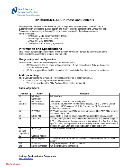
DP83848H-MAU-EK Purpose and ContentsThe purpose of the DP83848H-MAU-EK (EK) is to provide National Semiconductor Corp.'scustomers with a vehicle to quickly design and market systems containing the DP83848H chip. Customers are encouraged to copy EK components to expedite their design process.The EK contains:• DP83848H Media Attachment Unit (MAU)• Printed copy of this User's Guide• DP83848H MAU schematic• DP83848H MAU licensing agreementInformation and SpecificationsThis section contains specifications of the DP83848H MAU card, as well as a description of thecard's interfaces, connectors, jumpers and the LED.Usage setup and configurationPower for the DP83848H MAU is supplied via MII connector.•If 5V is supplied, the on-board voltage regulator, U5, will convert 5V to 3.3V for the device.J11 should be removed.•If 3.3V is supplied from the MII connector, J11 needs to be ON (See schematics for details). Address settings:The PMD address for the DP83848H Physical Layer device is set by jumper J4.•Default board setting for the PHY Address is 01•The board may be set to PHY Address 03 by adding jumper J4.Table of jumpers:Jumper Name FunctionJ1 MII MaleMII interfaceConnectorJ2 MII Header Alternative connection for MII signalsJ3A,B,C MDIO access J3 A to B should be ON for MII MDIO access, J3B to C should ON foron_board uMDIO access, J3 A, B, C should be OFF for externaluMDIO/FDI card useJ4 PHYAD1 PHY Address strap pin (PHY address = 01 when J4 is OFF, PHY address= 03 when J4 is ON)J5 MDIX_EN Auto_MDIX is enabled when J5 is OFF and disabled when J5 is ON.J6 LED_CFG Set LED configuration. When J6 is OFF and the chip is powered, a light onLED_LNK represents the presence of a link. When J6 is ON, the blinkinglight on LED_LNK represents link and activity. In both cases when there isno light on LED_LNK, this is an indication of absence of link.J7 RESET_N J7 ON will reset the deviceJ8 (Notpopulated)J9 Optional headerJ11 MII 3V3 option J11 should OFF for 5V MII supply and J11 should be ON for 3.3V MIIsupplyJ12 Pulse Jack Integrated Magnetic RJ-45 connectorJ15 MDIO connector On_board uMDIO connectionDP83848H MAU SpecificationOverviewThe DP83848H MAU is an NSC demo platform to allow customer evaluation of our device.While the DP83848H has many advanced and enticing features, this specific board is designed to demonstrate only a subset of those. The features chosen are the ones that the mainstream customers will use. Thus we have created an affordable, aesthetic platform to demonstrate the simplicity of designing in a National Semiconductor DP83848H.Target EnvironmentAny customer equipment that provides a standard IEEE 802.3, Clause 22 MII DTE interface; e.g. SmartBits/Netcom box.Features/GoalsThe DP83848H MAU features:•Intergrated magnetics•Minimum configuration requirements:o 2 PHY Addresses - 01h (default) or 03ho 2 LEDs – 1 power, 1 LED for LINKo Strap Options – MDIX_EN, LED_CFGo RESET_N jumper•Connections for the following interfaces:o MIl Interfaceo Integrated transformer RJ-45o Header for “ribbon cable” connection to MII•Standard PCB layout considerations with regards to clock, MII, and TD/RD•Single sided component placement•On-board clock – Crystal•On-board power supplied by MII connector only, jumper to configure 5v or 3.3v•On-board MDIO circuit•Low costMAU Block DiagramPCB Physical Layout requirements / Considerations•FR4 material•Trace impedance will be ensured by design:o Trace symmetry within differential pair (+/- 0.5”)o Differential impedance 100 ohms, +/- 5%o Adjacent differential pairs spacing > 2X distance within a differential pair, to minimize cross-talk and EMI•Trace length matching between differential pairs not required•Trace space will be 0.007”/0.008” minimum•Uniform supply & ground plane•Combination of through-hole and surface mount technology•Target size 2.0” (height), 3.0” (length)• 4 layers•Silk screen on two sidesMAU Interface requirements•System interface will be via the MII connector, and MII header•RJ-45 for network connection•On Board Serial Management circuitSoftware•No device specific software is required for this boardNational does provide the integrity utility; a diagnostic and configuration package at/appinfo/networks/ethernet_utility.htmlAdditional informationUpdated versions of the included material, related material can be found by going to or directly to design resources at/appinfo/networks/webench/dp83848.htmlNational Semiconductor Corporation2900 Semiconductor DriveSanta Clara, CA 95051, U.S.A.Tel: 1-800-272-9959Fax: 1-800-737-7018Email: support@WWW: National Semiconductor EuropeFax: (+49) 0-180-530 85 86Email: europe.support@Deutsch Tel: (+49) 0-180-530 85 85English Tel: (+49) 0-180-532 78 32National Semiconductor Asia PacificCustomer Response GroupTel: 65-254-4466Fax: 65-250-4466Email: sea.support@National Semiconductor Japan Ltd.Tel: 81-3-5620-6175Fax: 81-3-5620-6179Copyright © 2005 National Semiconductor Corporation.National Semiconductor and the National Semiconductor logo are registered trademarks of National Semiconductor Corporation. All other brand or product names are trademarks of their respective holders.分销商库存信息: NATIONAL-SEMICONDUCTOR DP83848H-MAU-EK。
RB751SL;中文规格书,Datasheet资料
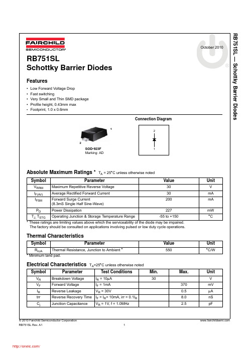
Absolute Maximum Ratings * T A = 25°C unless otherwise noted* These ratings are limiting values above which the serviceability of the diode may be impaired. The factory should be consulted on applications involving pulsed or low duty cycle operations.Thermal Characteristics* Minimum land pad.Electrical Characteristics T A =25°C unless otherwise notedSymbolParameterValueUnitV RRM Maximum Repetitive Reverse Voltage 30V I F(AV)Average Rectified Forward Current 30mA I FSM Forward Surge Current(8.3mS Single Half Sine-Wave)200mA P D Power Dissipation227mW T J, T STGOperating Junction & Storage Temperature Range-55 to +150°CSymbolParameterValueUnitR θJA Thermal Resistance, Junction to Ambient *550°C/WSymbolParameterTest ConditionsMin.Max.UnitV R Breakdown Voltage I R = 10μA 30V V F Forward Voltage I F = 1mA 370mV I R Reverse Leakage V R = 30V0.5μA trr Reverse Recovery Time I F = I R = 10mA, irr = 0.1I R8.0nS C jJunction CapacitanceV R = 1V, f = 1.0MHz2.5pFConnection Diagram2121SOD-923F Marking: ADThe following includes registered and unregistered trademarks and service marks, owned by Fairchild Semiconductor and/or its global subsidiaries, and is notAccuPower¥Auto-SPM¥Build it Now¥CorePLUS¥CorePOWER¥CROSSVOLT¥CTL¥Current Transfer Logic¥DEUXPEED®Dual Cool™ EcoSPARK®EfficientMax¥ESBC¥®Fairchild®Fairchild Semiconductor®FACT Quiet Series¥FACT®FAST®FastvCore¥FETBench¥FlashWriter®*FPS¥F-PFS¥FRFET®Global Power Resource SMGreen FPS¥Green FPS¥ e-Series¥G max¥GTO¥IntelliMAX¥ISOPLANAR¥MegaBuck¥MICROCOUPLER¥MicroFET¥MicroPak¥MicroPak2¥MillerDrive¥MotionMax¥Motion-SPM¥OptoHiT™OPTOLOGIC®OPTOPLANAR®®PDP SPM™Power-SPM¥PowerTrench®PowerXS™Programmable Active Droop¥QFET®QS¥Quiet Series¥RapidConfigure¥¥Saving our world, 1mW/W/kW at a time™SignalWise¥SmartMax¥SMART START¥SPM®STEALTH¥SuperFET®SuperSOT¥-3SuperSOT¥-6SuperSOT¥-8SupreMOS®SyncFET¥Sync-Lock™®*The Power Franchise®TinyBoost¥TinyBuck¥TinyCalc¥TinyLogic®TINYOPTO¥TinyPower¥TinyPWM¥TinyWire¥TriFault Detect¥TRUECURRENT¥*P SerDes¥UHC®Ultra FRFET¥UniFET¥VCX¥VisualMax¥XS™* Trademarks of System General Corporation, used under license by Fairchild Semiconductor.DISCLAIMERFAIRCHILD SEMICONDUCTOR RESERVES THE RIGHT TO MAKE CHANGES WITHOUT FURTHER NOTICE TO ANY PRODUCTS HEREIN TO IMPROVE RELIABILITY, FUNCTION, OR DESIGN. FAIRCHILD DOES NOT ASSUME ANY LIABILITY ARISING OUT OF THE APPLICATION OR USE OF ANY PRODUCT OR CIRCUIT DESCRIBED HEREIN; NEITHER DOES IT CONVEY ANY LICENSE UNDER ITS PATENT RIGHTS, NOR THE RIGHTS OF OTHERS. THESE SPECIFICATIONS DO NOT EXPAND THE TERMS OF FAIRCHILD’S WORLDWIDE TERMS AND CONDITIONS, SPECIFICALLY THE WARRANTY THEREIN, WHICH COVERS THESE PRODUCTS.LIFE SUPPORT POLICYFAIRCHILD’S PRODUCTS ARE NOT AUTHORIZED FOR USE AS CRITICAL COMPONENTS IN LIFE SUPPORT DEVICES OR SYSTEMS WITHOUT THE EXPRESS WRITTEN APPROVAL OF FAIRCHILD SEMICONDUCTOR CORPORATION.As used herein:1. Life support devices or systems are devices or systems which, (a) areintended for surgical implant into the body or (b) support or sustain life, and (c) whose failure to perform when properly used in accordance with instructions for use provided in the labeling, can be reasonably expected to result in a significant injury of the user. 2. A critical component in any component of a life support, device, orsystem whose failure to perform can be reasonably expected to cause the failure of the life support device or system, or to affect its safety or effectiveness.ANTI-COUNTERFEITING POLICYFairchild Semiconductor Corporation's Anti-Counterfeiting Policy. Fairchild's Anti-Counterfeiting Policy is also stated on our external website, , under Sales Support.Counterfeiting of semiconductor parts is a growing problem in the industry. All manufacturers of semiconductor products are experiencing counterfeiting of their parts. Customers who inadvertently purchase counterfeit parts experience many problems such as loss of brand reputation, substandard performance, failed applications, and increased cost of production and manufacturing delays. Fairchild is taking strong measures to protect ourselves and our customers from the proliferation of counterfeit parts. Fairchild strongly encourages customers to purchase Fairchild parts either directly from Fairchild or from Authorized Fairchild Distributors who are listed by country on our web page cited above. Products customers buy either from Fairchild directly or from Authorized Fairchild Distributors are genuine parts, have full traceability, meet Fairchild's quality standards for handling and storage and provide access to Fairchild's full range of up-to-date technical and product information. Fairchild and our Authorized Distributors will stand behind all warranties and will appropriately address any warranty issues that may arise. Fairchild will not provide any warranty coverage or other assistance for parts bought from Unauthorized Sources. Fairchild is committed to combat this global problem and encourage our customers to do their part in stopping this practice by buying direct or from authorized distributors.PRODUCT STATUS DEFINITIONSDefinition of TermsDatasheet Identification Product Status Definition分销商库存信息: FAIRCHILDRB751SL。