BZ-2RN770;中文规格书,Datasheet资料
07200;中文规格书,Datasheet资料

DRAWING NUMBER
PHONE (781) 821-8370
© 2011 DESCO INDUSTRIES INC.
Employee Owned
FAX (781) 575-0172
07200
DATE May 2011
/
分销商库存信息:
DESCO 07200
20"
18
"
Laundering Instructions:
If need be, this cover can be laundered. Use cool or warm water. Maximum temperature 120 °F. Do not use bleach, tumble dry on cool. Chair not included
Product marked with ESD protective symbol to identify used for ESD control “Fabric upholstered chairs accomplish this by using conductive fibers wovenห้องสมุดไป่ตู้into the fabric. The fabric is then connected through the components of the chair, through the cylinder, base and casters (or drag chain) to the floor.” [ESD Handbook TR20.20 Seating section 5.3.5.2 Types and Selection] If not otherwise noted, tolerance ±10% Specifications and procedures subject to change without notice
624N;中文规格书,Datasheet资料

ebm-papst St.Georgen GmbH&Co.KGHermann-Papst-Straße1D-78112St.GeorgenPhone+49772481-0Fax+49772481-1309info2@Nominal dataType624NNominal voltage VDC24Nominal voltage range VDC12..28Speed min-16100Power input W 2.2Min.ambient temperature°C-20Max.ambient temperature°C70Air flow m3/h40Sound power level B 4.7Sound pressure level dB(A)35ml=max.load·me=max.efficiency·fa=running at free air·cs=customer specs·cu=customer unitSubject to alterationsTechnical featuresGeneral description Particular design features:Rigid compression curve for high air flow at high counterpressure.Motor has very low structure-borne noise.Innovative impeller with winglets for low noise.Control inputs and alarm and speed signals available on request.General features:Material:fibreglass-reinforced plastic.Impeller PA,housing PBT.Electronic commutation completely integrated.Protected against reverse polarity and locking.Connection via single strands AWG22,TR64,bared and tin-plated.Air exhaust over bars.Rotational direction clockwise looking at rotor.Mass:85g.Mass0.085kgDimensions60x60x25mmMaterial of impeller Fiberglass-reinforced PA plasticHousing material Fiberglass-reinforced PBT plasticDirection of air flow Air exhaust over barsDirection of rotation Right,looking at rotorBearing Ball bearingsLifetime L10at40°C72500hLifetime L10at maximum35000htemperatureConnection line Single strands AWG22,TR64,bared and tin-plated.Motor protection Protected against reverse polarity and locking.Locked-rotor protection With electronic blocking and overload protectionApproval VDE,CSA,UL,CEProduct drawingCharts:Air flow分销商库存信息: EBM-PAPST624N。
AON7702中文资料
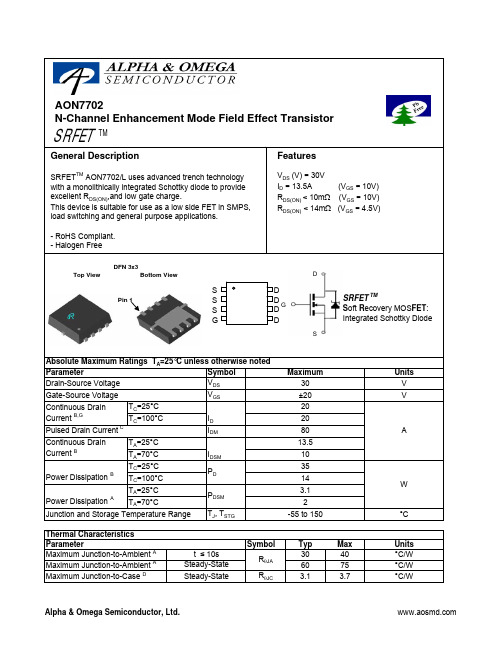
SymbolTyp Max 30406075R θJC 3.1 3.7°C/WThermal Characteristics ParameterUnits Maximum Junction-to-Ambient A t ≤ 10s R θJA °C/W °C/W Maximum Junction-to-Case DSteady-StateMaximum Junction-to-Ambient A Steady-State Absolute Maximum Ratings T A =25°C unless otherwise noted AON7702SDSRFET S Integrated Schottky DiodePin 1SymbolMin TypMaxUnits BV DSS 30V 100T J =55°C500I GSS 100nA V GS(th)1 1.63V I D(ON)80A810T J =125°C12151114g FS 21S V SD 0.380.5V I S6A C iss 23904250pF C oss 480pF C rss 180pF R g0.51 1.5ΩQ g (10v)3748nC Q g (4.5v)1621nC Q gs 9.3nC Q gd 5.5nC t D(on)9ns t r 14ns t D(off)32ns t f 16ns t rr 2938ns Q rr15nC 1503514COMPONENTS IN LIFE SUPPORT DEVICES OR SYSTEMS ARE NOT AUTHORIZED. AOS DOES NOT ASSUME ANY LIABILITY ARISING OUT OF SUCH APPLICATIONS OR USES OF ITS PRODUCTS. AOS RESERVES THE RIGHT TO IMPROVE PRODUCT DESIGN,FUNCTIONS AND RELIABILITY WITHOUT NOTICE.Drain-Source Breakdown Voltage On state drain currentI D =250µA, V GS =0V V GS =10V, V DS =5V V DS =30V, V GS =0VV DS =0V, V GS = ±20V Zero Gate Voltage Drain Current Gate-Body leakage current I DSS µA Body Diode Reverse Recovery Charge I F =13.5A, dI/dt=100A/µsBody Diode Reverse Recovery TimeV GS =10V, I D =13.5AReverse Transfer Capacitance I F =13.5A, dI/dt=100A/µsGate Threshold Voltage V DS =V GS I D =250µA Electrical Characteristics (T J =25°C unless otherwise noted)STATIC PARAMETERS ParameterConditions R DS(ON)Static Drain-Source On-ResistanceForward TransconductanceDiode Forward Voltage Maximum Body-Diode Continuous CurrentInput Capacitance Output Capacitance DYNAMIC PARAMETERS V GS =4.5V, I D =11AI S =1A,V GS =0V V DS =5V, I D =13.5Am ΩTurn-On Rise Time Turn-Off DelayTime V GS =10V, V DS =15V, R L =1.1Ω, R GEN =3ΩTurn-Off Fall TimeTurn-On DelayTime Gate Drain Charge V GS =0V, V DS =15V, f=1MHz SWITCHING PARAMETERS Total Gate Charge Gate Source Charge Gate resistanceV GS =0V, V DS =0V, f=1MHzTotal Gate Charge V GS =10V, V DS =15V, I D =13.5AA: The value of R θJA is measured with the device mounted on 1in 2 FR-4 board with 2oz. Copper, in a still air environment with T A =25°C. The value in any given application depends on the user's specific board design. B: Repetitive rating, pulse width limited by junction temperature.C. The R θJA is the sum of the thermal impedence from junction to lead R θJL and lead to ambient.D. The static characteristics in Figures 1 to 6 are obtained using <300 µs pulses, duty cycle 0.5% max.E. These tests are performed with the device mounted on 1 in 2 FR-4 board with 2oz. Copper, in a still air environment with T A =25°C. The SOA curve provides a single pulse rating.F. The current rating is based on the t ≤ 10s junction to ambient thermal resistance rating.G.The maximum current rating is limited by bond-wires.Rev0: Sept 2007。
ATC770中文说明书
DyniscoInstruments带有微处理器的ATC770压力/过程控制器安装和使用手册(中文版)本手册译自:DyniscoInstrumentsINSTALLATION & OPERATION MANUALATC 770 MICROPROCESSOR-BASEDPRESSURE/PROCESS CONTROLLER本中文版说明书力图在尽可能多的方面忠实于原英文说明书,但对准确性不做承诺。
如有任何疑问请参阅原英文说明书注意:本中文版说明书保有不先行通知即行修改的权利DyniscoInstrumentsATC770-0-2-3表快速入门1.安装. 按如下尺寸准备安装口。
.移开锁紧卡,以便将仪表从机壳中抽出。
.抓紧机壳将仪表抽出装在机壳上。
.将橡胶垫圈装在壳体。
.将机壳插入开好的安装口。
. 放入面板紧固件,将紧固螺丝旋入拧紧。
.将仪表插回机壳,直到听到喀的一声,表示安装到位。
2. 接线.按接线端子图所注连接传感器。
.连接控制执行设备。
.如带报警功能,连接报警.注意:报警2,3的出厂设置是高、反向动作;报警1是低禁止的。
.按图所示务必正确连接电源。
6.1 端子配置3.线性-远程S.P4.线性-远程S.P红→ 12.应变片信号+或线性+黑→ 13.应变片信号-或线性-橙→ 14.校正2白→ 16.激励+蓝/绿→ 17.激励-,校正121.控制输出 mA/V+22.控制输出 mA/V-23.远程复位24. 远程复位输出45.报警1,常开46. 报警1,公共端47.报警1,常闭48. 报警2,常开49. 报警2,公共端50.报警2,常闭51.报警3,公共端52.报警3, 常闭/常开53.100-240VAC(交流电)54.LN(交流零线)56.模拟输入中继输出 mA/V+57.模拟输入中继输出 mA/V-58.24VDC辅助电源输出+59.24VDC辅助电源输出+60.RS-485:A/A’61.RS-485:B/B’62.RS-485:数字输入公共端63.数字输入164.数字输入265.数字输入366.数字输入43. 设置量程.给仪表加电.上位显示窗将显示一个近零值。
NTMD4820NR2G;中文规格书,Datasheet资料

NTMD4820N Power MOSFET30 V, 8 A, Dual N −Channel, SOIC −8Features•Low R DS(on) to Minimize Conduction Losses •Low Capacitance to Minimize Driver Losses•Optimized Gate Charge to Minimize Switching Losses •Dual SOIC −8 Surface Mount Package Saves Board SpaceApplications•Disk Drives•DC −DC Converters •PrintersMAXIMUM RATINGS (T J = 25°C unless otherwise stated)RatingSymbol Value Unit Drain −to −Source Voltage V DSS 30V Gate −to −Source Voltage V GS ±20V Continuous Drain Current R q JA (Note 1)Steady StateT A = 25°C I D6.4AT A = 70°C 5.1Power DissipationR q JA (Note 1)T A = 25°C P D 1.28W Continuous Drain Current R q JA (Note 2)T A = 25°C I D 4.9A T A = 70°C 3.9Power Dissipation R q JA (Note 2)T A = 25°C P D 0.75W Continuous Drain Current R q JA t < 10 s (Note 1)T A = 25°CI D 8.0AT A = 70°C6.4Power Dissipation R q JA t < 10 s (Note 1)T A = 25°C P D 2.0W Pulsed Drain CurrentT A = 25°C,t p = 10 m sIDM 32A Operating Junction and Storage Temperature T J , T STG−55 to +150°C Source Current (Body Diode)I S 2.0A Single Pulse Drain −to −Source Avalanche Energy T J = 25C, V DD = 30 V, V GS = 10 V,I L = 11 A pk , L = 1.0 mH, R G = 25 W EAS 60.5mJ Lead Temperature for Soldering Purposes (1/8″ from case for 10 s)T L260°CTHERMAL RESISTANCE RATINGSRatingSymbol Max UnitJunction −to −Ambient – Steady State (Note 1)R q JA 97.5°C/W Junction −to −Ambient – t ≤10 s (Note 1)R q JA 62Junction −to −FOOT (Drain)R q JF 40Junction −to −Ambient – Steady State (Note 2)R q JA167.51.Surface −mounted on FR4 board using 1 inch sq pad size, 1 oz Cu.2.Surface −mounted on FR4 board using the minimum recommended pad size.N −Channel30 V27 m W @ 4.5 V20 m W @ 10 V R DS(on) Max I D Max V (BR)DSS 8 ADevice Package Shipping †ORDERING INFORMATIONNTMD4820NR2GSOIC −8(Pb −Free)2500/T ape & ReelSOIC −8CASE 751STYLE 114820N = Device CodeA = Assembly Location Y = YearWW = Work WeekG = Pb −Free Package†For information on tape and reel specifications,including part orientation and tape sizes, please refer to our Tape and Reel Packaging Specification Brochure, BRD8011/D.8MARKING DIAGRAM & PIN ASSIGNMENTS1G1S2G2D1D1D2D2GELECTRICAL CHARACTERISTICS(T J = 25°C unless otherwise noted)jkCharacteristic Symbol Test Condition Min Typ Max Unit OFF CHARACTERISTICSDrain−to−Source Breakdown Voltage V(BR)DSS V GS= 0 V, I D= 250 m A30V Drain−to−Source Breakdown Voltage Tem-perature CoefficientV(BR)DSS/T J26mV/°CZero Gate Voltage Drain Current I DSS VGS= 0 V,V DS= 24 V T J = 25°C 1.0m A T J = 100°C10Gate−to−Source Leakage Current I GSS V DS= 0 V, V GS= ±20 V±100nA ON CHARACTERISTICS (Note 3)Gate Threshold Voltage V GS(TH)V GS= V DS, I D= 250 m A 1.5 3.0V Negative Threshold Temperature Coeffi-cientV GS(TH)/T J 5.0mV/°CDrain−to−Source On Resistance R DS(on)V GS= 10 V I D= 7.5 A1520m WV GS= 4.5 V I D= 6.5 A2027Forward Transconductance g FS V DS= 1.5 V, I D= 7.5 A21S CHARGES, CAPACITANCES AND GATE RESISTANCEInput Capacitance C ISSV GS= 0 V, f = 1.0 MHz, V DS= 15 V 940pFOutput Capacitance C OSS225 Reverse Transfer Capacitance C RSS125Total Gate Charge Q G(TOT)V GS= 4.5 V, V DS= 15 V, I D= 7.5 A 7.7nCThreshold Gate Charge Q G(TH) 1.1Gate−to−Source Charge Q GS 3.3Gate−to−Drain Charge Q GD 3.2Total Gate Charge Q G(TOT)V GS= 10 V, V DS= 15 V, I D= 7.5 A15.2nC SWITCHING CHARACTERISTICS (Note 4)Turn−On Delay Time t d(ON)V GS= 10 V, V DD= 15 V,I D= 1.0 A, R G= 6.0 W 9.4nsRise Time t r 4.0 Turn−Off Delay Time t d(OFF)21 Fall Time t f 6.5 DRAIN−TO−SOURCE CHARACTERISTICSForward Diode Voltage V SD VGS = 0 VI D = 2.0 A T J = 25°C0.75 1.0V T J = 125°C0.59nsReverse Recovery Time t RRV GS = 0 V, d IS/d t = 100 A/m s,I S = 2.0 A 17.8Charge Time T a8.3Discharge Time T b9.5Reverse Recovery Time Q RR8.0nC PACKAGE PARASITIC VALUESSource Inductance L ST A = 25°C 0.66nHDrain Inductance L D0.20nH Gate Inductance L G 1.50nH Gate Resistance R G 1.5 3.0W 3.Pulse Test: pulse width v 300 m s, duty cycle v 2%.4.Switching characteristics are independent of operating junction temperatures.VDS, DRAIN −TO −SOURCE VOLTAGE (VOLTS)I D , D R A I N C U R R E N T (A M P S )Figure 1. On −Region CharacteristicsFigure 2. Transfer CharacteristicsV GS , GATE −TO −SOURCE VOLTAGE (VOLTS)Figure 3. On −Resistance vs. Gate −to −SourceVoltageI D , D R A I N C U R R E N T (A M P S )Figure 4. On −Resistance vs. Drain Current andGate VoltageFigure 5. On −Resistance Variation withTemperature T J , JUNCTION TEMPERATURE (°C)R D S (o n ), D R A I N −T O −S O U R C E R E S I S T A N C E (N O R M A L I Z E D )R D S (o n ), D R A I N −T O −S O U R C E R E S I S T A N C E (W )Figure 6. Drain −to −Source Leakage Currentvs. VoltageV DS , DRAIN −TO −SOURCE VOLTAGE (VOLTS)D S S I D, DRAIN CURRENT (AMPS)V GS , GATE −TO −SOURCE VOLTAGE (VOLTS)R D S (o n ), D R A I N −T O −S O U R C E R E S I S T A N C E (W )Figure 7. Capacitance VariationFigure 8. Gate −To −Source andDrain −To −Source Voltage vs. Total ChargeFigure 9. Resistive Switching Time Variation vs. Gate ResistanceFigure 10. Diode Forward Voltage vs. CurrentDRAIN −TO −SOURCE VOLTAGE (VOLTS)C , C A P A C I T A N C E (p F )V G S , G A T E -T O -S O U R C E V O L T A G E (V O L T S )Q G, TOTAL GATE CHARGE (nC)R G , GATE RESISTANCE (OHMS)t , T I M E (n s )T J , STARTING JUNCTION TEMPERATURE (°C)E A S , S I N G L E P U L S E D R A I N −T O −S O U R C E A V A L A N C H E E N E R G Y (m J )Figure 11. Maximum Rated Forward BiasedSafe Operating AreaV DS , DRAIN −TO −SOURCE VOLTAGE (VOLTS)I D , D R A I N C U R R E N T (A M P S )Figure 12. Maximum Avalanche Energy vs.Starting Junction TemperatureV DS , DRAIN-TO-SOURCE VOLTAGE (VOLTS)V SD , SOURCE −TO −DRAIN VOLTAGE (VOLTS)I S , S O U R C E C U R R E N T (A M P S )PACKAGE DIMENSIONSSOIC −8 NB CASE 751−07ISSUE AJNOTES:1.DIMENSIONING AND TOLERANCING PER ANSI Y14.5M, 1982.2.CONTROLLING DIMENSION: MILLIMETER.3.DIMENSION A AND B DO NOT INCLUDE MOLD PROTRUSION.4.MAXIMUM MOLD PROTRUSION 0.15 (0.006)PER SIDE.5.DIMENSION D DOES NOT INCLUDE DAMBAR PROTRUSION. ALLOWABLE DAMBARPROTRUSION SHALL BE 0.127 (0.005) TOTAL IN EXCESS OF THE D DIMENSION AT MAXIMUM MATERIAL CONDITION.6.751−01 THRU 751−06 ARE OBSOLETE. NEW STANDARD IS 751−07.DIM A MIN MAX MIN MAX INCHES4.805.000.1890.197MILLIMETERS B 3.80 4.000.1500.157C 1.35 1.750.0530.069D 0.330.510.0130.020G 1.27 BSC 0.050 BSC H 0.100.250.0040.010J 0.190.250.0070.010K 0.40 1.270.0160.050M 0 8 0 8 N 0.250.500.0100.020S5.806.200.2280.244MYM0.25 (0.010)YM0.25 (0.010)Z SXS____0.60.024ǒmm inchesǓSCALE 6:1*For additional information on our Pb −Free strategy and solderingdetails, please download the ON Semiconductor Soldering and Mounting Techniques Reference Manual, SOLDERRM/D.SOLDERING FOOTPRINT*STYLE 11:PIN 1.SOURCE 12.GATE 13.SOURCE 24.GATE 25.DRAIN 26.DRAIN 27.DRAIN 18.DRAIN 1ON Semiconductor and are registered trademarks of Semiconductor Components Industries, LLC (SCILLC). SCILLC reserves the right to make changes without further notice to any products herein. SCILLC makes no warranty, representation or guarantee regarding the suitability of its products for any particular purpose, nor does SCILLC assume any liability arising out of the application or use of any product or circuit, and specifically disclaims any and all liability, including without limitation special, consequential or incidental damages.“Typical” parameters which may be provided in SCILLC data sheets and/or specifications can and do vary in different applications and actual performance may vary over time. All operating parameters, including “Typicals” must be validated for each customer application by customer’s technical experts. SCILLC does not convey any license under its patent rights nor the rights of others. SCILLC products are not designed, intended, or authorized for use as components in systems intended for surgical implant into the body, or other applications intended to support or sustain life, or for any other application in which the failure of the SCILLC product could create a situation where personal injury or death may occur. Should Buyer purchase or use SCILLC products for any such unintended or unauthorized application, Buyer shall indemnify and hold SCILLC and its officers, employees, subsidiaries, affiliates,and distributors harmless against all claims, costs, damages, and expenses, and reasonable attorney fees arising out of, directly or indirectly, any claim of personal injury or death associated with such unintended or unauthorized use, even if such claim alleges that SCILLC was negligent regarding the design or manufacture of the part. SCILLC is an Equal Opportunity/Affirmative Action Employer. This literature is subject to all applicable copyright laws and is not for resale in any manner.PUBLICATION ORDERING INFORMATION分销商库存信息: ONSEMINTMD4820NR2G。
2N7002DW;中文规格书,Datasheet资料
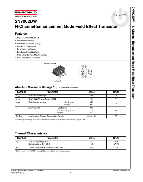
2N7002DW — N-Channel Enhancement Mode Field Effect Transistor 1Marking : 2N12N7002DW — N-Channel Enhancement Mode Field Effect TransistorElectrical Characteristics T C= 25°C unless otherwise notedOff Characteristics (Note1)On Characteristics (Note1)Dynamic CharacteristicsSwitching CharacteristicsNote1 : Short duration test pulse used to minimize self-heating effect .Symbol Parameter Test Condition MIN TYP MAX UnitsBV DSS Drain-Source Breakdown Voltage V GS = 0V, I D =10uA6078-V I DSS Zero Gate Voltage Drain Current V DS = 60V, V GS = 0VV DS = 60V, V GS = 0V, @T C = 125°C -0.0017 1.0500uA I GSSGate-Body LeakageV GS = ±20V, V DS = 0V-0.2±10nAV GS(th)Gate Threshold VoltageV DS = V GS , I D = 250uA1.0 1.762.0V R DS(ON)Satic Drain-Source On-Resistance V GS = 5V, I D = 0.05A,V GS = 10V, I D = 0.5A, @T j = 125°C -- 1.62.537.513.5ΩI D(ON)On-State Drain Current V GS = 10V, V DS = 7.5V 0.5 1.43-A g FSForward TransconductanceV DS = 10V, I D = 0.2A80356.5-mSC iss Input Capacitance V DS = 25V, V GS = 0V, f = 1.0MHz-37.850pF C oss Output Capacitance-12.425pF C rssReverse Transfer Capacitance- 6.57.0pFt D(ON)Turn-On Delay Time V DD = 30V, I D = 0.2A, V GEN = 10V R L = 150Ω, R GEN = 25Ω- 5.8520nst D(OFF)Turn-Off Delay Time-12.5202N7002DW — N-Channel Enhancement Mode Field Effect Transistor2N7002DW — N-Channel Enhancement Mode Field Effect Transistor2N7002DW — N-Channel Enhancement Mode Field Effect TransistorTRADEMARKSThe following are registered and unregistered trademarks and service marks Fairchild Semiconductor owns or is authorized to use andis not intended to be an exhaustive list of all such trademarks.DISCLAIMERFAIRCHILD SEMICONDUCTOR RESERVES THE RIGHT TO MAKE CHANGES WITHOUT FURTHER NOTICE TO ANY PRODUCTS HEREIN TO IMPROVE RELIABILITY, FUNCTION, OR DESIGN. FAIRCHILD DOES NOT ASSUME ANY LIABILITY ARISING OUT OFTHE APPLICATION OR USE OF ANY PRODUCT OR CIRCUIT DESCRIBED HEREIN; NEITHER DOES IT CONVEY ANY LICENSE UNDER ITS PATENT RIGHTS, NOR THE RIGHTS OF OTHERS. THESE SPECIFICATIONS DO NOT EXPAND THE TERMS OF FAIRCHILD’S WORLDWIDE TERMS AND CONDITIONS, SPECIFICALLY THE WARRANTY THEREIN, WHICH COVERS THESE PRODUCTS.LIFE SUPPORT POLICYFAIRCHILD’S PRODUCTS ARE NOT AUTHORIZED FOR USE AS CRITICAL COMPONENTS IN LIFE SUPPORT DEVICES OR SYSTEMS WITHOUT THE EXPRESS WRITTEN APPROVAL OF FAIRCHILD SEMICONDUCTOR CORPORATION.As used herein:1. Life support devices or systems are devices or systemswhich, (a) are intended for surgical implant into the body, or(b) support or sustain life, and (c) whose failure to performwhen properly used in accordance with instructions for useprovided in the labeling, can be reasonably expected to resultin significant injury to the user.2. A critical component is any component of a life supportdevice or system whose failure to perform can be reasonablyexpected to cause the failure of the life support device orsystem, or to affect its safety or effectiveness.PRODUCT STATUS DEFINITIONSDefinition of TermsACEx®Build it Now™CorePLUS™CROSSVOLT™CTL™Current Transfer Logic™EcoSPARK®Fairchild®Fairchild Semiconductor®FACT Quiet Series™FACT®FAST®FastvCore™FPS™FRFET®Global Power Resource SMGreen FPS™Green FPS™ e-Series™GTO™i-Lo™IntelliMAX™ISOPLANAR™MegaBuck™MICROCOUPLER™MicroFET™MicroPak™Motion-SPM™OPTOLOGIC®OPTOPLANAR®®PDP-SPM™Power220®Power247®POWEREDGE®Power-SPM™PowerTrench®Programmable Active Droop™QFET®QS™QT Optoelectronics™Quiet Series™RapidConfigure™SMART START™SPM®STEALTH™SuperFET™SuperSOT™-3SuperSOT™-6SuperSOT™-8SyncFET™The Power Franchise®TinyBoost™TinyBuck™TinyLogic®TINYOPTO™TinyPower™TinyPWM™TinyWire™µSerDes™UHC®UniFET™VCX™Datasheet Identification Product Status DefinitionAdvance Information Formative or In DesignThis datasheet contains the design specifications for product development.Specifications may change in any manner without notice.Preliminary First ProductionThis datasheet contains preliminary data; supplementary data will be pub-lished at a later date. Fairchild Semiconductor reserves the right to makechanges at any time without notice to improve design.No Identification Needed Full ProductionThis datasheet contains final specifications. Fairchild Semiconductor reservesthe right to make changes at any time without notice to improve design.Obsolete Not In ProductionThis datasheet contains specifications on a product that has been discontin-ued by Fairchild semiconductor. The datasheet is printed for reference infor-mation only.Rev. I302N7002DW N-Channel Enhancement Mode Field Effect Transistor 2N7002DW分销商库存信息: FAIRCHILD2N7002DW。
74271622S;中文规格书,Datasheet资料

5.1 5.0 4.02012-06-272012-04-302010-05-19SStSStSMuSStSMu-Würth Elektronik eiSos GmbH & Co. KGEMC & Inductive SolutionsMax-Eyth-Str. 174638 WaldenburgGermanyTel. +49 (0) 79 42 945 - 0A Dimensions: [mm]Additional FeaturesSafety key to lock/ unkock74271D2 General Properties:Ferrite core Ferrite core Ferrite core Plastic housing Plastic housing Test cable Test cablePropertiesMaterial Initial permeability Curie temperatureColourFlammability ClassificationApplicable cable Applicable cable lengthµi T CValue 4 W 620620150Black UL94-V0AWG26165Unit°Cmm Tol.typ.typ.F Typical Impedance Characteristics:I Cautions and Warnings:The following conditions apply to all goods within the product series of WE-STAR GAPof Würth Elektronik eiSos GmbH & Co. KG:General:All recommendations according to the general technical specifications of the data sheet have to be complied with.The disposal and operation of the product within ambient conditions which probably alloy or harm the component surface has to be avoided.The packaging of the product is to encase the needed humidity of the plastic housing. To ensure the humidity level, the products have to be stored in this delivered packaging. If not, the products are losing their humidity. In this case you can re-condition the components according to the internal standard WE1883 to ensure the necessary humidity in the plastic.To ensure the operating mode of the product, the ambient temperature at processing (when the part will be mounted on the cable) has to be in the range of 15 to 25 °C.Before mounting, the part should be stored for one hour in this condition.The responsibility for the applicability of customer specific products and the use in a particular customer design is always within the authority of the customer. All technical specifications for standard products do also apply for customer specific products.Direct mechanical impact to the product and the forcible closing of this shall be prevented as the ferrite material of the ferrite body or the pla-stic housing could flake or in the worst case it could break.Product specific:Follow all instructions mentioned in the datasheet, especially:•The cable diameter must be pointed out, otherwise no warranty will be sustained.•Violation of the technical product specifications such as exceeding the nominal rated current will result in the loss of warranty.1. General Customer ResponsibilitySome goods within the product range of Würth Elektronik eiSos GmbH & Co. KG contain statements regarding general suitability for certain application areas. These statements about suitability are based on our knowledge and experience of typical requirements concerning the are-as, serve as general guidance and cannot be estimated as binding statements about the suitability for a customer application. The responsibi-lity for the applicability and use in a particular customer design is always solely within the authority of the customer. Due to this fact it is up to the customer to evaluate, where appropriate to investigate and decide whether the device with the specific product characteristics described in the product specification is valid and suitable for the respective customer application or not.2. Customer Responsibility related to Specific, in particular Safety-Relevant ApplicationsIt has to be clearly pointed out that the possibility of a malfunction of electronic components or failure before the end of the usual lifetime can-not be completely eliminated in the current state of the art, even if the products are operated within the range of the specifications.In certain customer applications requiring a very high level of safety and especially in customer applications in which the malfunction or failure of an electronic component could endanger human life or health it must be ensured by most advanced technological aid of suitable design of the customer application that no injury or damage is caused to third parties in the event of malfunction or failure of an electronic component.3. Best Care and AttentionAny product-specific notes, warnings and cautions must be strictly observed.4. Customer Support for Product SpecificationsSome products within the product range may contain substances which are subject to restrictions in certain jurisdictions in order to serve spe-cific technical requirements. Necessary information is available on request. In this case the field sales engineer or the internal sales person in charge should be contacted who will be happy to support in this matter.5. Product R&DDue to constant product improvement product specifications may change from time to time. As a standard reporting procedure of the Product Change Notification (PCN) according to the JEDEC-Standard inform about minor and major changes. In case of further queries regarding the PCN, the field sales engineer or the internal sales person in charge should be contacted. The basic responsibility of the customer as per Secti-on 1 and 2 remains unaffected.6. Product Life CycleDue to technical progress and economical evaluation we also reserve the right to discontinue production and delivery of products. As a stan-dard reporting procedure of the Product Termination Notification (PTN) according to the JEDEC-Standard we will inform at an early stage about inevitable product discontinuance. According to this we cannot guarantee that all products within our product range will always be available. Therefore it needs to be verified with the field sales engineer or the internal sales person in charge about the current product availability ex-pectancy before or when the product for application design-in disposal is considered.The approach named above does not apply in the case of individual agreements deviating from the foregoing for customer-specific products.7. Property RightsAll the rights for contractual products produced by Würth Elektronik eiSos GmbH & Co. KG on the basis of ideas, development contracts as well as models or templates that are subject to copyright, patent or commercial protection supplied to the customer will remain with Würth Elektronik eiSos GmbH & Co. KG.8. General Terms and ConditionsUnless otherwise agreed in individual contracts, all orders are subject to the current version of the “General Terms and Conditions of Würth Elektronik eiSos Group”, last version available at .J Important Notes:The following conditions apply to all goods within the product range of Würth Elektronik eiSos GmbH & Co. KG:分销商库存信息: WURTH-ELECTRONICS 74271622S。
NCV7703D2G;NCV7703D2R2G;NCV7703GEVB;中文规格书,Datasheet资料

V −0.3 to 40
−1
Output Pin OUTx (DC) (AC), t < 500 ms, IOUTx > −2 A
V −0.3 to 40
−1
Pin Voltage (Logic Input pins, SI, SCLK, CSB, SO, EN, VCC)
Output Current (OUTx) (DC) (AC) (50 ms pulse, 1 s period)
5
SI
Serial Input
6
SCLK
Serial Clock
7
GND*
Ground. Connect all grounds together.
8
GND*
Ground. Connect all grounds together.
9
SO
Serial Output
10
EN
Enable. Logic high wakes the IC up from a sleep mode.
OUT3
14 1
SOIC−14 D2 SUFFIX CASE 751A
MARKING DIAGRAM
14
NCV7703G AWLYWW
1
NCV7703 = Specific Device Code
A
= Assembly Location
WL = Wafer Lot
Y
NCV7703
Triple Half-Bridge Driver with SPI Control
The NCV7703 is a fully protected Triple Half−Bridge Driver designed specifically for automotive and industrial motion control applications. The three half−bridge drivers have independent control. This allows for high side, low side, and H−Bridge control. H−Bridge control provides forward, reverse, brake, and high impedance states. The drivers are controlled via a standard SPI (Serial Peripheral Interface). This device is fully compatible with ON Semiconductor’s NCV7708 Double Hex Driver.