ELC-10PR中文资料
虹润OHR-PR10系列简易PLC中文一体机使用说明书

一、产品介绍二、技术参数使用说明书OHR-PR10系列简易PLC中文一体机 Hong Run Precision Instruments Co., LtD.虹润OHR-PR10系列简易PLC中文一体机是一款中文文本编辑的逻辑控制继电器,集逻辑判断、输出、延时、计时、计数、跳转、循环等功能于一体。
适用于公共区域照明、绿化带灌溉、养殖投喂控制、设备逻辑控制与时序控制。
★易于操作的控制器现场编程,中文代码操作,易掌握。
★经济型小型自动控制器8路开关量输入(NPN/PNP/干接点)和8路开关量输出(2路单刀双掷,6路常开点)。
★电源故障措施当断电时,EEPROM可以备份程序和系统设置。
★自由逻辑编程内置99个计数器、99个计时器,18组编程操作组,可自由逻辑编程,每组可编辑159行程序。
★便于维护采用人机界面来显示用户指定的信息、日期、时间或其它数据。
★黑暗环境下背光更长背光自动切断时间可设为1~99分钟,或者可将背光设为常亮状态。
★编程安全性可设置密码来保护程序。
★远程监视功能通过RS-485通信进行远程监视。
★供电可选100~240VAC和12~24VDC电源可供选择。
★导轨式或壁挂式安装标准的35mmDIN导轨卡式安装,操作简单。
额定参数电源电压功率消耗工作温度相对湿度保存温度保护等级性能规格参数LCD显示屏操作按钮日历/时间绝缘电阻介电强度技术规格参数开关量输入开关量输出通讯输出功能块AC100~240V(50/60Hz);DC12~24V100VAC:7VA 最大 240VAC:10VA 最大 12/24VDC:4VA 最大-10~50℃10%~90%RH(无冷凝)-10~60℃IP20(安装在控制面板上)2.8英寸点阵式液晶显示,带LED背光8个按钮(4个光标按钮和4个操作按钮)精度:±15s/月(25℃±2℃)不小于20MΩ(500VDC下);在电源端子和所有输出端子之间;在不同输出端子之间。
紫光同创产品手册 PANGO Product Guide

紫光同创产品手册PANGO Product Guide2023关于我们官方合作伙伴业务范围芯驿电子科技(上海)有限公司,成立于2012年,总部位于上海松江临港科技城,是一家车载智能产品和FPGA 技术方案公司,拥有“AUMO”和“ALINX”两大品牌,其中AUMO 品牌专注车载智能产品,ALINX 品牌专注于FPGA 产品和方案定制。
经历十年发展,公司产品已经远销海外30多个国家。
2018年,公司通过高新技术企业认证,并通过ISO9001质量体系认证;2019年,荣获上海市松江区九亭镇“科技创新奖”;2020年,荣获上海市“专精特新企业“称号;2021年,申请通过上海市科技型中小企业技术创新资金项目,通过了国家级科技型中小企业认定,并通过了高新技术企业认证复审;2022年获得上海市张江国家自主创新示范区专项发展资金并通过“上海市创新型中小企业”认证。
ALINX 是全球的FPGA 芯片龙头企业XILINX 官方合作伙伴,国内FPGA 芯片龙头企业紫光同创官方合作伙伴,同时作为百度AI 合作伙伴,为百度定制了国产AI飞桨系统的Edgeboard 系列边缘设备。
通过多年的研发投入,已经推出100多款FPGA SoM 模组和配套板卡,积累了1000多家企业批量用户,上万个独立开发者,市场占有率遥遥领先。
通过产品+定制化服务的经营方式,ALINX 将继续加大对产品研发和技术研究的投入,不断与垂直行业客户合作,聚焦高端设备领域,协助客户解决行业的技术难题。
主要聚焦于FPGA + AI 解决方案,FPGA 国产化,FPGA 开发套件, ALINX 自有品牌产品。
公司提供的设计解决方案涉及人工智能、自动驾驶、轨道交通、半导体、5G 通信、医疗设备、工业互联、仪器仪表、数据中心、机器视觉、视频图像处理等行业。
紫光同创国内唯一的FPGA 板卡官方合作伙伴,XILINX 官方重要合作伙伴,百度AI合作伙伴。
轨道交通医疗设备半导体自动驾驶智能制造AI人工智能产品定制简介产品定制业务主要针对企业和研究院所,根据客户的需求进行产品的软硬件设计。
FPGA可编程逻辑器件芯片EP4CE10F17C8N中文规格书

P IPELINED V ISION P ROCESSOR (PVP)PVP F UNCTIONAL D ESCRIPTIONThe angle φ is calculated to five bits of resolution (11.25°) and an accuracy of ±0.25°. Mathematically, the angle is a signed value. However, since the angle is always zero-extended when output to 16-bit or 32-bit buses, it can also be interpret as an unsigned binning value.Figure 30-17:PMA Angle BinningThe PMA sets the angle to 0x08 (+90°) if the x input value is 0 and the y input is a positive value and to 0x18 (-90°) if the y input is negative. If both, x and y are zero, the PMA outputs 0x1F by convention.Other than data flow configuration, the PMA block does not have any control or status registers. Both of its inputs can be individually configured to receive data from any of the convolution blocks or from either input formatter.NOTE :Care is required in that both inputs are timed consistently and are not subject to non-matchinglatency in up front pipeline configuration.The PMA block has three output ports. If PMA is enabled, all three 32-bit ports are always active as follows. •Port 0 drives the 16-bit unsigned magnitude. The upper 16 bits are always driven as zeros.•Port 1 drives the 5-bit angle value. The upper 27 bits are always driven as zeros.•Port 2 drives a combined format. The lower 16 bits contain the magnitude, bits 16 to 20 drive the angle,and the upper ones are always zero. The Port 2 signal is not only good for being streamed to system memory. The PEC block and THCn blocks have special functionality to deal with this format.The table and figure show the PMA block data flow and PVP block connections. For a graphical overview of all PVP block interconnections, see Configuring Pipe Structure.Table 30-33:CNV2 Block ConnectivityCNV2 Block I/O Data Format PVP Block ConnectSelections Port ConnectInput 0 s16 IPF0IPF1CNV0CNV1CNV30, 1, 2 0, 1, 2 0Input 1 n/a n/a n/a Output 0s32 (Result)CNV0, CNV1, CNV3,PMA, ACU, PEC, THC0,THC1, IIM0, IIM1.OPF0, OPF1, OPF2,OPF3n/aOutput 1 n/a n/a n/a Output 2 n/a n/a n/aTable 30-34:CNV3 Block ConnectivityCNV3 Block I/O Data Format PVP Block ConnectSelections Port ConnectInput 0 s16 IPF0IPF1CNV0CNV1CNV20, 1, 2 0, 1, 2 0Input 1 n/a n/a n/a Output 0s32 (Result)CNV0, CNV1, CNV2,PMA, ACU, PEC, THC0,THC1, IIM0, IIM1.OPF0, OPF1, OPF2,OPF3n/aOutput 1 n/a n/a n/a Output 2 n/a n/a n/aFigure 30-12:CNV RCCC Received From SensorWhen CNV1 receives a Bayer or a RCCC data stream, red pixel substitution performs convolution/correlation, shift and saturate operation only on the red pixel. The blue and green pixels (the clear pixels) are passed to the output without modification. In this mode, the PVP_CNVn_CTL.SAT32 control bit must be set to zero. Only then can accumulation results saturate to 16 bits and match the data range of the unmodified 16-bit clear pixels. All pixels are sign-extended to 32 bits on the output.Figure 30-13:CNV RCCC Convolution Kernel FlowThe red pixel substitution mode is enabled by the PVP_CNVn_CTL.RFRMT0 bit. The PVP_CNVn_CTL.RFRMT1 bit distinguishes between Bayer Type 1 or Type 2 configuration.There are multiple strategies for substituting the red pixel in an RCCC data stream. The CNV1 blockallows for many types of mean value generation that interpolate the missing clear value (in place of the red pixel). The following figure provides an overview of the most prominent convolution kernels.*OQVU$POWPMVUJPO,FSOFM 4I J G U F S 4B U V S B U J P O 3$$@5:1& @&/"#-& CJU3$$@5:1& @&/"#-& CJU 0VUQVU5PHHMF 'MJQ 'MPQT GPS 3PX BOE $PMVNO。
Berkeley VC-10 产品说明书

Q U I C K R E F E R E N C E G U I D E Berkeley®VC®–10Vacuum CurettageSystemCustomer Service888-524-72662B E R K E L EY ®VC ®–10S ET U P Q U I C K R E F E R E N C ESetup for 3/8”collection tubing set with 4–12mm Vacurette ®cannulas1.Place the primary and secondarycollection canisters 003984-901or003987-901in the receptacles.Place lids on top of the canistersmaking sure they are securelysnapped in place.2.Attach the short end of theDisposa-Filter 54298to thevacuum port of the pump andthe long end to the “PUMP”porton the secondary canister lid.3.Attach the 18”series connectinghose 20714to the “PATIENT”porton the secondary collection canisterlid and to the “PUMP”port on theprimary collection canister lid.4.Insert a SafeTouch tissue trap003853-902into the “PATIENT”port on the primary collectioncanister lid.Alternatively,a gauzesack 003997-901can beutilized.B E R K E L EY ®VC ®–10S ET U P Q U I C K R E F E R E N C E 37.Attach a rigid straight,curved or flexible Vacurette cannula to the patient end of the collection tubing set.A cannula up to 12mm can be used with the 3/8”tubing.A 14mm cannula can be used with an adapter 003696.5.Close off all open lid ports withthe large blue sealing caps.6.Insert the male end of a sterile3/8”collection tubing set 23116into the top of the tissue trap ordirectly to the “PATIENT”port onthe lid if a gauze sack is used.Note:Flexible cannulas are available separately or preattached to tubing sets.*1416For the primary canister and lid use ref BKC-506.This lid has an1/2”“PATIENT”port opening(A)and comes with a preattached gauze sack(B).Use the1/2”collection tubing set ref BKT-506and a14or16mm cannula.Follow steps above as for the3/8”tubing set eliminating the tissue trap and inserting the male end of the1/2”tubing set directly into the“PATIENT”port(C).Helpful Tip(for both3/8”and1/2”sets):To prevent the secondary canister from filling prematurely,an aspiration filter(A) 003905-901can be attached to the underside of the“PUMP”port on the primary collection canister lid(B).4B E R K E L EY®VC®–10S ET U P Q U I C K R E F E R E N C EB E R K E L EY ®VC ®–10S ET U P Q U I C K R E F E R E N C E 510(Refer to VC-10Instructions for Use and Technical Manual 80807for completeinstructions)Figure ADepressing the left side of the switch (Symbol I )turns the vacuum on immediately.Depressing the right side of the switch activates the foot pedal control (SymbolTo start the vacuum the foot pedal must be depressed.Note:must be continually pressed to maintain vacuum level.Be sure the foot pedal is properly connected prior to activation.1.Attach power cord to appropriate powerreceptacle and assemble accessorycomponents.2.Turn the unit on by activating the 3-positionpower switch on the front panel (Figure A ).The vacuum can be turned on by eitherpressing the switch on the front panel to theleft or by pressing the foot pedal with theswitch pressed to the right.6B E R K E L EY ®VC ®–10S ET U P Q U I C K R E F E R E N C E1.Open the front door of the storagecompartment to access the foot pedalreceptacle connection.Enlarged view ofreceptacleconnection.2.Insert the foot pedal connector into thereceptacle until a click sound is heard.To remove connector,press thumb-slide downward.4.Close door and place foot pedal on floor.After use,foot pedal can be stored incompartment without disconnecting.3.Pull cable straight down and fitin the molded curve.1.Close all accessory openings by occludingthe tip of the Vacurette cannula or theinlet at end of collection tubing handleprior to attaching the cannula and closing the slip-ring on the collection set handle.2.Turn the vacuum control knob clockwiseto increase vacuum.(Figure B)3.Verify that the vacuum gauge has stabi-lized after each knob adjustment.4.Once the desired vacuum setting hasbeen reached and the gauge has stabi-lized,the procedure may begin. Note:•The unit is preset at the factoryin the fully counterclockwise positionfor minimum vacuum.•The vacuum gauge is color codedas follows(in cm Hg):0–7.4white,7.5–50red,50–60yellow,60–75green.(Figure C)•The maximum attainable vacuum withthe valve fully clockwise open,at sealevel,is approximately73cm Hg.Thereis a reduction of vacuum by2.6cm Hgper1,000feet(8.5mm Hg per100meters)of elevation above sealevel.Figure B Figure CB E R K E L EY®VC®–10S ET U P Q U IC K R E F E R E N C E7This is designed as a quick reference guide only.This guide is not a substitute for reading and learning theentire Operator’s Manual and/or Instructions For Use(IFU)provided with the Berkeley®VC®–10Vacuum CurettageSystem.Gyrus ACMI cannot encourage or recommend anyactions that deviate from or are not covered by the IFU.Fora complete list of warnings,cautions,and instructions on theuse,care,and maintenance of the Berkeley®VC®–10Vacuum Curettage System,please refer to the Berkeley®VC®–10Vacuum Curettage System User Manual providedwith your unit.Gyrus ACMIⅢ136Turnpike RoadⅢSouthborough,MA01772USA PHONE:888.524.7266/508.804.2600ⅢFAX:508.804.2624ⅢWEB:©2009Olympus Corporation of America.All rights reserved.™and®Trademarks and Registered Trademark, respectively,of Olympus or its Subsidiaries in the U.S.and/or other countries of the world.PI321-0609 Subject to change without notice.。
RM10C混合记录仪规格说明书

RM10C HYBRIDRECORDER OUTLINERM10C is 100mm calibrated hybrid recorder in a 144x144DIN front panel and short depth of 150mm case housing.The recorder has versatility of universal input and scale inwide ranges and flexibility of user-reconfigurable uniquefunctions. RM10C offers 1, 2 continuous pen and 6 dotpoint models.FEA TURESShort case depth size of 150mmIP65: Dust-proof, Water-proofWide LED with 18mm heights displayAllows user-selected consumablesRS-232C communication interface instandard specificationsUL, C-UL, CE approvedWeights only 1.5kg (Multipoint type)Optional portable housing case availableSPECIFICA TIONSz Input signalDC voltage:± 10, 0 ~ 20, 0 ~ 50, ± 200 mV DC, ± 1, 0 ~ 5,± 10 V DCThermocouple:B, R, S, K, E, J, T, C, Au-Fe, N, PR40-20, PLII, U, L Resistance temperature detector: Pt100, JPt100DC current: 4 ~ 20mA DC(with external shunt resistor: 250Ω<Charged: HMSU3081A11>) z PerformanceAccuracy: See RANGE TABLEDead band: Within 0.2% (Pen Model only)Input impedance:10MΩ min. in mV, TC input;200kΩ min. in mV, TC input (with burnout protection);1MΩ min. in Voltage input;250Ω (External shunt resister) in mA inputAllowable signal source resistance:10kΩ max. in mV, TC input;100Ω max. in mV, TC input (with burnout protection);1kΩ max. in Voltage input;10Ω max. per line in RTD inputNormal mode reduction ratio: 60dB min. (50/60 ± 0.1Hz) Common mode reduction ratio: 140dB min. (50/60 ± 0.1Hz) Isolation resistance: 0.5kV DC 20MΩ min. between theeach terminal and grounding terminal Dielectric strength:1.5kV AC for 1 minute between power terminal andgrounding terminal;0.5kV AC for 1 minute between input terminal andgrounding terminal;0.2kV AC for 1 minute between the input terminalsInter channel maximum noise voltage:200 V AC at 50/60 HzVibration resistance: 10 ~ 60Hz 1m/s2 max.Shock resistance: 2m/s2 max.Clock precision: ± 50ppm max.Chart feed accuracy: ± 0.1% max.z StructureMounting: Panel mountAllowable backward inclination: Within 30°Material (Color):Case, Polycarbonate (Black), Glass 10% UL94-V2;Door, Polycarbonate, UL94-V2 (Clear)Dust-proof, Water-proof(Complies with the IEC529-IP65) z Power Supply V oltagePower voltage (rated): 100 ~ 240V AC Power voltage: 85 ~ 264V ACFrequency (rated): 50/60HzFrequency: 45 ~ 65Hzz Normal Operating ConditionsAmbient temperature: 0 ~ 50°C Ambient humidity: 20 ~ 80%RH Supply voltage: 85 ~ 264V ACz Alarm (Relay output is optional)Alarm types: 2 types(H,L),4 levels/channelAlarm output: 250 V AC, 3 A max. (resistance load) 125 V DC, 0.5 A max.(resistance load) 30 V DC, 3 A max.(resistance load) Hysteresis width: 0.5 ± 0.2 % Setting accuracy: ± 0.5 % Outputs:Pen Model, 3 point (Built-in option, normally open); Multipoint Model, 6 point (Built-in option, normally open)z Safety Standard and EMI Standard Electrical safety:IEC1010-1,UL3101-1 installation category II and pollution degree 2. UL3101-1Emissions: EN55011 Group1 Class A Immunity: EN50082-2z Communication Interface RS-232C (Standard): 1200, 2400, 4800, 9600 RS-485 (Option): 1200, 2400, 4800, 9600z DI functionFunction Description Chart Feed Start/Stop Close: Starts Open: Stops Change Chart Speed Close: Chart speed 1 Open: Chart speed 2 Comment Print Prints programmed characters(Multipoint model is up to 16characters per line. Pen model is up to 12 characters per line.)Manual Print Close: Start to print Date and Time Print Close: Start to printUp to 3 functions among above can be selected in one recorder.z OptionChart sensor: Detects paper-out to output an alarm.INDIVIDUAL SPECIFICA TIONSBlock Item Pen Model Multi point Model Measuring Point 1, 2 6 Input Sampling 125ms 10s/6chInput Unit Display Interval 2.5s 2.5sRecording Form Disposable felt penPrinting Form Wire dot (one color ink ribbon) Wire dot with 6-color ink ribbonRecording Width 100 mmStep Response 1.0s max. to 95% of step-wise input - Dot Print Interval - 10s/ch (Note 2) Chart Paper Length : 16m, Width : 114 mm Folding width : 40 mm (Note3) Chart Speed 5, 10, 15, 20, 25, 30, 40, 50, 60, 75, 80, 90, 100,120, 150, 160, 180, 200, 240, 300, 360, 375, 450, 600, 720, 750, 900, 1200, 1500, 1800, 2400, 3000, 3600, 4500, 4800, 5400, 6000, 7200, 9000, 10800, 12000 mm/h0, 1, 2, 3, 4, 5, 10, 15, 20, 25, 30, 40, 50, 60,75, 80, 90, 100,120, 150, 160, 180, 200, 240, 300, 360, 375, 450, 600, 720, 750, 900, 1200, 150 mm/h (Analog recording is notdone during the chart speed setting 0 mm/h.)Recording Color (Note1) 1 pen (Red), 2 pen (Green)No.1 (Purple), No.2 (Red), No.3 (Green),No.4 (Blue), No.5 (Brown), No.6 (Black) Record & Printer Printing Color Purple Purple, Red, Green, Blue, Brown, Black Weight 1 pen: 2.0kg max., 2 pen: 2.5kg max, 1.5kg max. Power Consumption 30V A max. (at 100V AC) 25V A max. (at 100V AC)(Note 1) User-changeable arbitrary colors with set-up configuration. (Note 2) User-selective interval from 10, 20, 30 and 60 seconds. (Note 3) Clean Chart Paper: Length 12 mMEASUREMENT RANGEThe junction compensation accuracy is not calculated into digital readout accuracy and recording accuracy . The junction compensation accuracy is based on operating conditions: T emperature, 23 ± 2°C; Humidity , 55 ± 10%RH; Power source 85 ~ 264V AC; Frequency , 50/60Hz ± 1%; Warm-up time 30 minutes min.; No effect of vibration and shock of over recorder’s resistibility .Junction compensation accuracy: B, R, S, Au-Fe, PR40-20 ± 1°CK, E, J, T , C, N, PLII, U, L ± 0.5°CMeasurementDigital AnalogType RangeMeasurementrangeAccuracy Max.ResolutionAccuracy- 10.00 ~ 10.00mV ±(0.2% of rdg + 3digits) 10µV0.00 ~ 20.00mV ±(0.2% of rdg + 3digits) 10µV 0.00 ~ 50.00mV ±(0.2% of rdg + 2digits) 10µV - 200.0 ~ 200.0mV ±(0.2% of rdg + 3digits) 100µV - 1.000 ~ 1.000V ±(0.1% of rdg + 3digits) 1mV0.000 ~ 5.000V±(0.2% of rdg + 2digits)1mV - 10.00 ~ 10.00V ±(0.3% of rdg + 3digits) 10mV DC Voltage/ Current Input4 ~ 20mA ±(0.2% of rdg + 2digits) 0.01mADigital accuracy ±(0.3% of span)B 0.0 ~ 1820.0°C ±(0.15% of rdg + 1°C) (Note 1) R1 0.0 ~ 1760.0°C ±(0.15% of rdg + 1°C) (Note 2) R2 0.0 ~ 1200.0°C ±(0.15% of rdg + 0.8°C) (Note 2) S 0.0 ~ 1760.0°C ±(0.15% of rdg + 1°C) (Note 2) K1 - 200.0 ~ 1370.0°C ±(0.15% of rdg + 0.7°C) (Note 3) K2 - 200.0 ~ 600.0°C ±(0.15% of rdg + 0.4°C) (Note 3) K3 - 200.0 ~ 300.0°C ±(0.15% of rdg + 0.3°C) (Note 3) E1 - 200.0 ~ 800.0°C ±(0.15% of rdg + 0.5°C) E2 - 200.0 ~ 300.0°C ±(0.15% of rdg + 0.4°C) E3 - 200.0 ~ 150.0°C ±(0.15% of rdg + 0.3°C)J1 - 200.0~ 1100.0°C ±(0.15% of rdg + 0.5°C) (Note 4) J2 - 200.0 ~ 400.0°C ±(0.15% of rdg + 0.4°C) (Note 4)J3 - 200.0 ~ 200.0°C ±(0.15% of rdg + 0.3°C) (Note 4) T1 - 200.0 ~ 400.0°C ±(0.15% of rdg + 0.5°C) (Note 4) T2 - 200.0 ~ 200.0°C ±(0.15% of rdg + 0.4°C) (Note 4) C 0.0 ~ 2320.0°C ±(0.15% of rdg + 1°C) 0.1°CAu-Fe 1 .0 ~ 300.0K ±(0.15% of rdg + 1K) (Note 5) 0.1KN 0.0 ~ 1300.0°C ±(0.15% of rdg + 0.7°C) PR40-20 0.0 ~ 1880.0°C ±(0.15% of rdg + 1°C (Note 6) PLII 0.0 ~ 1390.0°C ±(0.15% of rdg + 0.7°C) U - 200.0 ~ 400.0°C ±(0.15% of rdg + 0.5°C) (Note 7) Thermo- couple L - 200.0 ~ 900.0°C ±(0.15% of rdg + 0.5°C) (Note 7) 0.1°CDigital accuracy ±(0.3% of span)Pt100-1 - 200.0 ~ 650.0°C ±(0.15% of rdg + 0.3°C)Pt100-2 - 200.0 ~ 200.0°C ±(0.15% of rdg + 0.2°C)JPt100-1 - 200.0 ~ 630.0°C ±(0.15% of rdg + 0.3°C) ResistanceT emperatureDetectorJPt100-2 - 200.0 ~ 200.0°C ±(0.15% of rdg + 0.2°C)0.1°CDigital accuracy ±(0.3% of span)Note 1: 400 ~ 600°C: ± 2°CA range under a span of 400°C: Accuracy is out of guaranteeNote 2: 0 ~ 100°C: ± 3.7°C 100 ~ 300°C, ± 1.5°C Note 3: - 200 ~ -100°C: ± (0.15% of rdg + 1°C) Note 4: - 200 ~ -100°C: ± (0.15% of rdg + 0.7°C) Note 5: 1 ~ 20 K: ±2.4 KNote 6: 0 ~ 300°C: ± 37.6°C 300 ~ 800°C, ±18.8°C Note 7: - 200 ~ -100°C: ± (0.15% of rdg + 0.7°C)STANDARD FUNCTIONSItem Description Analog recording Pen Models: Continuous pen tracingMulti point Model: Dot printing with 6-color ribbon cartridgeDigital display Indicates channel no., processvariable, date, chart speed, alarm setpoint in front display.Logging print Prints date, time, scale, chart speed,each channel’s process variable andengineering unit at a programmedinterval.List print Prints chart speed, type of input, range,engineering unit, alarm set point,comment print status, Printingdescription, logging print ON/OFFconfiguration, ZONE recordingconfiguration, point focus configurationEngineering list print Prints configuration of channel/tag print switch, alarm print, logging print ON/OFF, reference time, interval, alarm hysteresis, burnout protection, scaling print ON/OFF, DI function (option)Affix print (Multipoint Model) Prints Channel number besides analog recording line.Manual print Prints measured data by the front keyoperation. Analog recording stopsduring manual printing.Skip (Multipoint model) Abandon dot print of inputs as required.Programming Programs chart speed, alarm setpoint, logging print interval, skip, dateand time.Memory Backup Back-up for clock by built-in lithiumbattery for 10 years, 5 years inunpowered state.A non-volatile memory storesconfiguration and calibration data. Alarm Sets 2 types (H, L) of alarms perchannel. Sets a total of 4 levels. Chart Speed Selects Chart speed from 41 types. Clock Indication Indicates Y ear, Month, Day, Hour andMinute. Sets the year in A.D, andadjusts leap year automatically.Self Diagnostics Occurring some type of the defect toindicate “ERROR”.Scaling Indicates and record the input of aunification signal etc. is changed intothe engineering scales. CONFIGURABLE FUNCTIONSFunction Description Burnout protection Sets pointer at over 100% perinputs when input becomesopen for T/C or ±50mV max.input.T ag Number T ag number up to 5 charactersfor pen models/7 characters formultipoint model per channelcan be programmed, and printsat logging print.T emperatureCompensationInside/outside of referencejunction compensation (DE/DHconnection) can be specified.Copy Function Channel configuration data canbe copied to another channel.Input offset Input offset per channel can beprogrammed.ZONE Recording Recording on the chart track inspecified range per channel.Point focus recording Recording by point focus to1-crease line per channel.Decade Recording •IndicatingRecords and indicates up to 5decades. 2 figures of effectivenumber to indicate and print.Alarm print Prints time, channel number,setting number and type ofalarm in alarming.Alarm recovery print Prints recovery time, recoverychannel number, settingnumber and type of alarm atrecovery.Record start/end print Prints time and comment(“Start” or “End”) when recordbeginning or end.Square root Square root available.Integration Sum, balance, average amongchannels can be integrated.Damping(Pen Model)Digital filtering for measureddata (PV) in unsteady process.Filter constant range ability:1.0000 to 0.0001Formula is: k = 0.64/T Ik = Filter constantT I= 99.5% dampingAlarm Hysteresis Width Alarm hysteresis width can beprogrammed at 0% FS or 0.5%FS.DIMENSIONSPanel Cutout (mm)TERMINAL ARRANGEMENTMultipoint ModelPen ModelLN 1A 2 C 2 A 1 C 3 A 4 C 4A 3 C 5 A 6 C 6 A 5 C 4 +B4- B 4 A 5+B 5 - B 5 A 6+B 6- B 6 A 1 + B 1 - B1 A2 + B 2 - B 2 A 3+B 3- B3 ASG R D T D +– D I C O M D I 3 D I2 D I 1 LN1A 2 C 2 A 1 C 3 A 3 C 1+B 1-B 1A 2+B 2-B 2ASG R D T D + –D I C O M D I 3 D I2 D I 1T h e r m o c o u p l e i n p u t+-R T D i n p u tm A i n p u t m V , V i n p u t + + +A B bS h unt resistor R2 5 0Ω <Charged HMSU3081A11>+ - + - --Power GroundLN AC I N 7max.(Panel thickness)25150(Unit = mm)1 4 41 4 43 . 52 . 5CH, NO.DA T ARUN M E NU P RINT F E E D E NT200 min.200 m i n .138 138 –0+1 –0+1MODEL CODE NUMBER(Note 1) Combination of RS-232C and RS-485 unavailable.(Note 2) Nos. of relay outputs:6 point recorder 6 relays; Pen recorder 3 relaysCAUTIONDo not install this device before consulting instruction manualSpecifications are subject to change without notice.For further information, a quotation or a demonstration please contact to:Head Office / Factory Saitama, JAP ANSales Offices T okyo, Osaka, Nagoya, Kyushu, T ohokuURL http://www.ohkura.co.jp/e-mail (in English) ******************.jpPrinted in Japan: Aug. 2006。
FPGA可编程逻辑器件芯片EP3C10E144I7N中文规格书
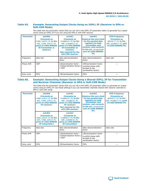
Table 65.Example: Generating Output Clocks Using an IOPLL IP (Receiver in DPA or Soft-CDR Mode)This table lists the parameter values that you can set in the IOPLL IP parameter editor to generate four output clocks using an IOPLL IP if you are using the DPA or soft-CDR receiver .Parameter outclk0(Connects aslvds_clk[1:0] to the ext_lvds_clk[1:0]ports of LVDS SERDES IP transmitter or receiver)outclk1(Connects as loaden[1:0] to theext_loaden[1:0]ports of LVDS SERDES IP transmitter or receiver)Not required for the soft-CDR receiver.outclk4(Used as the core clock for the parallel data registers for both transmitter and receiver, and connects to the ext_coreclock port of LVDS SERDES IP)VCO Frequency (Connects as phout[7:0] to the ext_vcoph[7:0] port of LVDS SERDES IP)Frequency data rate data rate/serialization factordata rate/serialization factor data rate Phase shift 180°[(deserialization factor -1)/deserialization factor]x 360°180/serialization factor (outclk0 phase shift divided by the serialization factor)—Duty cycle 50%100/serialization factor 50%—Table 66.Example: Generating Output Clocks Using a Shared IOPLL IP for Transmitter and Receiver Channels (Receiver in DPA or Soft-CDR Mode)This table lists the parameter values that you can set in the IOPLL IP parameter editor to generate six output clocks using an IOPLL IP . Use these settings if you use transmitter channels shared with receiver channels in DPA or soft-CDR mode.Parameter outclk0(Connects aslvds_clk[1:0] to the ext_lvds_clk[1:0]ports of LVDS SERDES IP receiver)outclk1(Connects as loaden[1:0] to theext_loaden[1:0]ports of LVDS SERDES IP receiver)Not required for the soft-CDR receiver.outclk4(Used as the core clock for the parallel data registers for both transmitter and receiver, and connects to the ext_coreclock port of LVDS SERDES IP)VCO Frequency (Connects as phout[7:0] to the ext_vcoph[7:0] ports of LVDS SERDES IP)outclk2(Connects as lvds_clk[1:0] to theext_lvds_clk[1:0]ports of LVDS SERDES IP transmitter)outclk3(Connects asloaden[1:0] to the ext_loaden[1:0]ports of LVDS SERDES IP transmitter)Frequencydata rate data rate/serialization factor data rate/serialization factor data rate Phase shift 180°[(deserialization factor -1)/deserialization factor]x 360°180/serialization factor (outclk0 phase shift divided by the serialization factor)—Duty cycle 50%100/serialization factor 50%—4.Intel Agilex High-Speed SERDES I/O ArchitectureUG-20214 | 2021.04.05Send Feedback4.5.3. Connection between IOPLL IP and LVDS SERDES IP in External PLL ModeFigure 73.Non-DPA or DPA LVDS Receiver Interface with the IOPLL IP (without LVDS transmitter in the same sub-bank)Figure 74.Non-DPA or DPA LVDS Receiver Interface with the IOPLL IP (with LVDS transmitter in the same sub-bank)Figure 75.Soft-CDR LVDS Receiver Interface with the IOPLL IP (without LVDS transmitter in the same sub-bank)4.Intel Agilex High-Speed SERDES I/O ArchitectureUG-20214 | 2021.04.05Send FeedbackFigure 76.Soft-CDR LVDS Receiver Interface with the IOPLL IP (with LVDS transmitter in the same sub-bank)Figure 77.LVDS Transmitter Interface with the IOPLL IPThe ext_coreclock port is automatically enabled in the LVDS SERDES IP in externalPLL mode. The Intel Quartus Prime compiler outputs error messages if this port is not connected as shown in the preceding figures.Related InformationUsing an External PLL on page 1314.6. LVDS SERDES IP Initialization and ResetDuring device initialization, the clock reference must be stable while the PLL is locking to it to avoid corruption of the PLL output clock phase shifts. If the PLL output clock phase shifts are incorrect, data transfer between the high-speed LVDS and low-speed parallel domain can fail and causes corrupted data.After you have initialized the IP in DPA or non-DPA mode, you can perform word boundaries alignment using the bitslip control signal.Note: Intel requires you to include the Reset Release Intel FPGA IP in your design to hold your application logic in the reset state until the entire FPGA fabric is in user mode.For more information about the Reset Release Intel FPGA IP, refer to the Intel Agilex Configuration User Guide: Including the Reset Release Intel FPGA IP in Your Design in the related information.4.Intel Agilex High-Speed SERDES I/O ArchitectureUG-20214 | 2021.04.05Send Feedback。
C1010中文资料
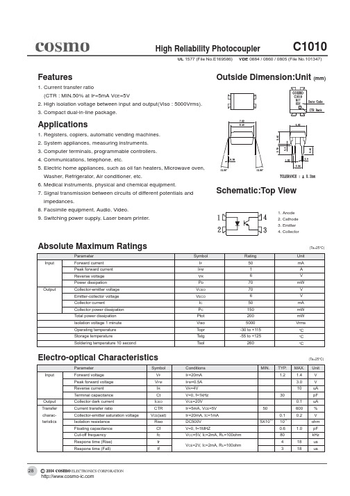
Schematic:Top View
Absolute Maximum Ratings
Parameter Input Forward current Peak forward current Reverse voltage Power dissipation Output Collector-emitter voltage Emitter-collector voltage Collector current Collector power dissipation Total power dissipation Isolation voltage 1 minute Operating temperature Storage temperature Soldering temperature 10 second Symbol IF IFM VR PD VCEO VECO IC PC Ptot Viso Topr Tstg Tsol Rating 50 1 6 70 70 6 50 150 200 5000 -30 to +115 -55 to +125 260 Unit mA A V mW V V mA mW mW Vrms °C °C °C
Collector Current Ic (mA)
Forward Current IF (mA)
Ambient Temperature Ta (°C)
Ambient Temperature Ta (°C)
c
2004
cosmo ELECTRONICS CORPORATION
Fig.7 Relative Current Transfer Ratio vs. Ambient Temperature
FPGA可编程逻辑器件芯片EP4CE10E22C8N中文规格书
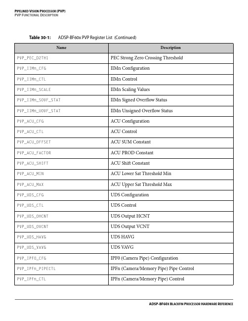
Table 30-1:ADSP-BF60x PVP Register List (Continued)Name DescriptionPVP_PEC_D2TH1PEC Strong Zero Crossing Threshold PVP_IIMn_CFG IIMn ConfigurationPVP_IIMn_CTL IIMn ControlPVP_IIMn_SCALE IIMn Scaling ValuesPVP_IIMn_SOVF_STAT IIMn Signed Overflow StatusPVP_IIMn_UOVF_STAT IIMn Unsigned Overflow StatusPVP_ACU_CFG ACU ConfigurationPVP_ACU_CTL ACU ControlPVP_ACU_OFFSET ACU SUM ConstantPVP_ACU_FACTOR ACU PROD ConstantPVP_ACU_SHIFT ACU Shift ConstantPVP_ACU_MIN ACU Lower Sat Threshold MinPVP_ACU_MAX ACU Upper Sat Threshold MaxPVP_UDS_CFG UDS ConfigurationPVP_UDS_CTL UDS ControlPVP_UDS_OHCNT UDS Output HCNTPVP_UDS_OVCNT UDS Output VCNTPVP_UDS_HAVG UDS HAVGPVP_UDS_VAVG UDS V AVGPVP_IPF0_CFG IPF0 (Camera Pipe) ConfigurationPVP_IPFn_PIPECTL IPFn (Camera/Memory Pipe) Pipe Control PVP_IPFn_CTL IPFn (Camera/Memory Pipe) ControlTable 30-1:ADSP-BF60x PVP Register List (Continued)Name Description PVP_CNVn_C40C41CNVn Coefficients 4,0 and 4,1 PVP_CNVn_C42C43CNVn Coefficients 4,2 and 4,3 PVP_CNVn_C44CNVn Coefficient 4,4PVP_CNVn_SCALE CNVn Scaling FactorPVP_THCn_CFG THCn ConfigurationPVP_THCn_CTL THCn ControlPVP_THCn_HFCNT THCn Histogram Frame Count PVP_THCn_RMAXREP THCn Max RLE ReportsPVP_THCn_CMINVAL THCn Min Clip ValuePVP_THCn_CMINTH THCn Clip Min ThresholdPVP_THCn_CMAXTH THCn Clip Max ThresholdPVP_THCn_CMAXVAL THCn Max Clip ValuePVP_THCn_TH0THCn Threshold Value 0PVP_THCn_TH1THCn Threshold Value 1PVP_THCn_TH2THCn Threshold Value 2PVP_THCn_TH3THCn Threshold Value 3PVP_THCn_TH4THCn Threshold Value 4PVP_THCn_TH5THCn Threshold Value 5PVP_THCn_TH6THCn Threshold Value 6PVP_THCn_TH7THCn Threshold Value 7PVP_THCn_TH8THCn Threshold Value 8PVP_THCn_TH9THCn Threshold Value 9P IPELINED V ISION P ROCESSOR (PVP)PVP F UNCTIONAL D ESCRIPTIONADSP-BF60x PVP Interrupt List PVP_THCn_HCNT7_STATTHCn Histogram Counter Value 7PVP_THCn_HCNT8_STATTHCn Histogram Counter Value 8PVP_THCn_HCNT9_STATTHCn Histogram Counter Value 9PVP_THCn_HCNT10_STATTHCn Histogram Counter Value 10PVP_THCn_HCNT11_STATTHCn Histogram Counter Value 11PVP_THCn_HCNT12_STATTHCn Histogram Counter Value 12PVP_THCn_HCNT13_STAT THCn Histogram Counter Value 13PVP_THCn_HCNT14_STATTHCn Histogram Counter Value 14PVP_THCn_HCNT15_STATTHCn Histogram Counter Value 15PVP_THCn_RREP_STATTHCn Number of RLE Reports PVP_PMA_CFG PMA ConfigurationTable 30-2:ADSP-BF60x PVP Interrupt List Interrupt List Description Interrupt ID DMA Channel Sensitivity PVP0 Camera Pipe DataOut B DMA Channel11138LEVEL PVP0 Camera Pipe DataOut C DMA Channel11239LEVEL PVP0 Camera Pipe StatusOut DMA Channel 11340LEVEL PVP0 Camera Pipe Control In DMA Channel 11441LEVELPVP0 Status 0115LEVEL PVP0 Memory Pipe DataOut DMA Channel 11642LEVELTable 30-1:ADSP-BF60x PVP Register List (Continued)Name Description。