MC33874BPNA;MC33874BPNAR2;中文规格书,Datasheet资料
SD387EVKNOPB;中文规格书,Datasheet资料
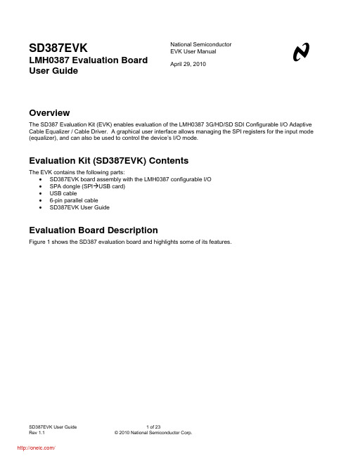
SD387EVKLMH0387 Evaluation Board User Guide National Semiconductor EVK User ManualApril 29, 2010OverviewThe SD387 Evaluation Kit (EVK) enables evaluation of the LMH0387 3G/HD/SD SDI Configurable I/O Adaptive Cable Equalizer / Cable Driver. A graphical user interface allows managing the SPI registers for the input mode (equalizer), and can also be used to control the device’s I/O mode.Evaluation Kit (SD387EVK) ContentsThe EVK contains the following parts:•SD387EVK board assembly with the LMH0387 configurable I/O•SPA dongle (SPIÆUSB card)• USB cable•6-pin parallel cable• SD387EVK User GuideEvaluation Board DescriptionFigure 1 shows the SD387 evaluation board and highlights some of its features.FIGURE 1. SD387 Evaluation BoardInputs and Outputs: BNC_IO Input/Output, SDI Input, and SDO OutputThe bidirectional I/O (J1) is a 75Ω BNC connector. When the LMH0387 is configured as an input, the input signal on the BNC_IO pin should conform to the SMPTE 424M, SMPTE 292M, or SMPTE 259M standards. When the LMH0387 is configured as an output, the BNC_IO pin will drive SMPTE SDI signal levels (800 mV P-P into 75Ω).The SDI input connectors (J2 and J3) are 50Ω SMA connectors. This cable driver input includes a 100Ω differential termination resistor (R5) at the LMH0387 device and is optimized for 100Ω differential input.The SDO output connectors (J4 and J5) are 50Ω SMA connectors. When using only one side of this equalizer output pair, the other side should be terminated with a 50Ω SMA termination. For example, when only using theSDO output, SDO¯¯¯¯ should be terminated with a 50Ω SMA termination.DC Power ConnectorsThe VCC and GND power connectors should be powered with a DC input voltage of 3.3V ± 5% (3.6V maximum).JP2 ControlsCD ¯¯¯JP2 allows monitoring of the Carrier Detect (CD¯¯¯ ) at the BNC_IO pin while in the input mode (equalizer). CD ¯¯¯ is asserted low when an input signal is detected at the BNC_IO pin, and high when no input signal is present. TX_ENJP2 allows control of the TX_EN pin to enable or disable the cable driver. The LMH0387 TX_EN pin has aninternal pullup to enable the cable driver by default, so this pin may be left unconnected when using the LMH0387 in the output mode. To disable the cable driver, place a jumper to tie TX_EN to GND. When using the LMH0387 in the input mode, the cable driver must be disabled by tying TX_EN low. TX_EN may optionally be controlled via the GUI using the SPA dongle as described below. SD/HD¯¯¯ JP2 allows control of the SD/HD¯¯¯ pin for setting the slew rate for the BNC_IO pin while the LMH0387 is in the output mode (cable driver). This pin may be connected to GND for the faster HD/3G slew rate or connected to V CC for theslower SD slew rate. The LMH0387 SD/HD¯¯¯ pin has an internal pulldown to enable the HD/3G slew rate by default.SPI Header (JP1)JP1 is the SPI (Serial Peripheral Interface) header. It allows access to the SPI pins (SS ¯¯¯ , MISO, MOSI, and SCK) to control the SPI registers of the LMH0387 equalizer. To use the SPI interactive GUI, plug the 6-pin parallel cable between this header and JP7 on the SPA dongle to connect the pins one-for-one as shown in Table 1. The SPA dongle requires special software and must be connected to the PC via the USB – see the Software Setup section.TABLE 1. SPI Connections between SD387 and SPA DongleSD387 JP1 SPA Dongle JP7 Pin # Name Pin # Name1 GND Æ 1 GND2 SCK Æ 2 MCK3 MOSI Æ 3 MOSI4 MISO Æ 4 MOSI5 SS Æ 5 SS6 GND Æ 6 GNDCarrier Detect LED (D1)D1 shows the status of Carrier Detect at the LMH0387 equalizer input. This LED is GREEN when an input signal has been detected at the BNC_IO pin, and OFF when no input is detected.SPA Dongle DescriptionThe SPA dongle is required to use the SPI interactive GUI. The SPA dongle connects between the LMH0387 SPI pins and the USB input of a PC. The SPA dongle is shown in Figure 2. JP7 is the SPI Header. The SPA dongle is powered through the USB, and the D1 LED is RED when the SPA dongle is connected to a PC via the USB to indicate the board is powered.FIGURE 2. SPA DongleFigure 3 shows the connection between the SD387 and the SPA dongle. For proper operation, the SPI pins must be connected between the SD387 JP1 and the SPA dongle JP7. Optionally, a single wire may be connected between the SD387 TX_EN pin (JP2) and the SPA dongle PA0 (J7) to enable software control of the LMH0387 cable driver enable functionality, and allow the GUI to fully control the LMH0387 I/O Mode as described on page 8. If this connection is not used, then the TX_EN can be controlled manually with a jumper.FIGURE 3. SD387 Connection to SPA DongleSoftware SetupSystem RequirementsOperating System:Windows XP or VistaUSB: 2.0InstallationDownload the latest software from the LMH0387 Evaluation Board page. Extract the ALPF_monthdayyear_major version_minor version.exe” (ex. ALPF_04062010_128_0002.exe) file to a temporary location that can be deleted later.Make sure the SPA dongle is not connected to the PC. The following installation instructions are for the Windows XP Operating System.Install the ALP softwareExecute the ALP Setup Wizard program called “ALPF_monthdayyear_major version_minor version.exe” (ex. ALPF_04062010_128_0002.exe) that was extracted to a temporary location.There are 7 steps to the installation once the setup wizard is started:1. Select the “Next” button.2. Select “I accept the agreement” and then select the “Next” button.3. Select the location to install the ALP software and then select the “Next” button.4. Select the location for the start menu shortcut and then select the “Next” button.5. There will then be a screen that allows the creation of a desktop and Quick Launch icon. After selectingthe desired choices select the “Next” button.6. Select the “Install” button, and the software will then be installed to the selected location.7. Uncheck “Launch Analog LaunchPAD” and select the “Finish” button. The ALP software will start if“Launch Analog LaunchPAD” is checked, but it will not be useful until the USB driver is installed.Connect JP1 of the SD387 evaluation board to JP7 of the SPA dongle via the 6-pin parallel cable as shown in Table 1. Power on the SD387 evaluation board with a 3.3 VDC power supply. Connect the SPA dongle to the PC with the USB cable. The “Found New Hardware Wizard” will open on the PC. Proceed to the next section to install the USB driver.Install the USB driverThere are 6 steps to install the USB driver:1. Select “No, not at this time” then select the “Next” button.2. Select “Install from a list or specific location” then select the “Next” button.3. Select “Search for the best driver in these locations”. Uncheck “Search removable media” and check“Include this location in the search”.4. Browse to the Install Directory which is typically located at “C:\Program Files\National SemiconductorCorp\Analog LaunchPAD\vx.x.x\Drivers” and select the “Next” button. Windows should find the driver.5. Select “Continue Anyway”.6. Select the “Finish” button.The software installation is complete. The ALP software may now be launched, as described in the next section.Software DescriptionStartupMake sure all the software has been installed and the hardware is powered on and connected to the PC. Execute “Analog LaunchPAD” from the start menu. The default start menu location is “Programs\National Semiconductor Corp\Analog LaunchPAD vx.x.x\Analog LaunchPAD”.The application should come up in the state shown in Figure 4 below. If it does not, see “Trouble Shooting” at the end of this document. Click on “LMH0387 – Nano” to select the device and open up the device profile and its associated tabs.FIGURE 4. ALP Startup Screen for the LMH0387Information TabThe Information tab is shown in Figure 5.FIGURE 5. LMH0387 Information TabFunctional TabThe Functional tab is the main tab of the GUI and presents a high level view of the LMH0387 equalizer, as shownin Figure 6.I/O Mode Controlprovided an additional wire is connected between the SD387 TX_EN and theSPA dongle PA0, as shown in Figure 3. The connection between TX_EN andPA0 allows software control of the LMH0387 cable driver enable functionality.If the SD387 TX_EN is not connected to the SPA dongle PA0, then TX_ENmay be controlled manually with a jumper and the I/O Mode Control will have no effect on the LMH0387 cable driver.The default LMH0387 I/O Mode setting is the Input (Rx) Mode, or equalizer mode. This default setting allows full control of the LMH0387 equalizer. The three I/O modes are described below.Input (Rx) Mode: Configures the LMH0387 for the input mode (equalizer enabled and cable driver disabled). This is the default setting. The LMH0387 equalizer is set to auto sleep, and if TX_EN is connected to PA0, then PA0 will drive TX_EN low to disable the LMH0387 cable driver. If this TX_EN Æ PA0 connection is not made, then the LMH0387 cable driver should be manually disabled by setting a jumper to tie TX_EN to GND.Output (Tx) Mode: Configures the LMH0387 for the output mode (cable driver enabled and equalizer disabled). The LMH0387 equalizer is forced to sleep. If TX_EN is connected to PA0, then PA0 will drive TX_EN high to enable the LMH0387 cable driver. If this TX_EN Æ PA0 connection is not made, then the LMH0387 cable drivershould be manually enabled by pulling the jumper between TX_EN and GND (TX_EN should be open).Tx Loopback Mode: Configures the LMH0387 for the output mode with a loopback path (cable driver andequalizer both enabled). The LMH0387 equalizer is set to auto sleep. If TX_EN is connected to PA0, then PA0 will drive TX_EN high to enable the LMH0387 cable driver. If this TX_EN Æ PA0 connection is not made, then theLMH0387 cable driver should be manually enabled by pulling the jumper between TX_EN and GND (TX_EN should be open). In this mode, the cable driver output on the BNC_IO pin is looped back to the LMH0387 equalizeroutputs (SDO and SDO¯¯¯¯ ), so the cable driver output may be observed both at BNC_IO pin and at the SDO/SDO ¯¯¯¯ output pins.The Cable Driver TX_EN indicator shows the current status of the TX_EN control (only if TX_EN is connected to PA0). It is GREEN to indicate TX_EN is driven high and the LMH0387 cable driver is enabled, or OFF to indicate TX_EN is driven low and the LMH0387 cable driver is disabled.Equalizer Sleep Mode and Carrier DetectThe Equalizer Sleep Mode control shows the status of the Sleep Mode register bits and allows control over the sleep mode. The Equalizer Sleep Mode settings are as follows:On: Force the equalizer into sleep mode (powered down) regardless of whether there is an input signal or not.Off: Disable sleep mode (force equalizer to stay enabled).Auto: Sleep mode active when no input signal detected (default mode).The Equalizer Sleep Status indicator shows the current sleep status of the equalizer. It is GREEN to indicate sleeping or OFF to indicate not sleeping.The Carrier Detect shows the status of the BNC_IO input carrier detect. It is GREEN to indicate the input signal is present or OFF to indicate the input signal is absent.Equalizer Output SwingThe Equalizer Output Swing control shows the current value of the LMH0387 equalizer output amplitude and allows adjustment in 100 mV increments from 400 mV P-P to 800 mV P-P . The default setting is 700 mV P-P . The Equalizer Output Swing may be set either by clicking on the “+” or “-” buttons, or by grabbing and spinning the “handle” on the knob for a quick adjustment.Equalizer Output OffsetThe Equalizer Output Offset control shows the current value of the LMH0387 equalizeroutput common mode voltage and allows adjustment in 200 mV increments from 1.05Vto 1.85V. At the “Max” setting, the outputs are referenced to the positive supply and theoutput common mode is 2.1V. The default setting is 1.25V. The Equalizer Output Offsetmay be set either by clicking on the “+” or “-”buttons, or by grabbing and spinning the“handle” on the knob for a quick adjustment.Equalizer Output MuteThe Equalizer Output Mute indicator shows the mute status, and the button may be used totoggle the mute function. The indicator is GREEN to indicate mute (equalizer outputs aremuted) and OFF to indicate normal mode (outputs are not muted).Extended 3G Reach ModeThe Extended 3G Reach Mode indicator shows the status of the Extended 3G ReachMode register bit, and the button may be used to toggle this register bit. The indicator isGREEN when the bit is set for extended 3G reach mode, and OFF when the equalizer isset for normal mode. Note that the indicator shows the status of the register bit – notwhether the device is actually in extended 3G reach mode or not. If extended 3G reachmode is set, the equalizer will remain in this mode until the input cable is physically changed or power is cycled. For example, extended 3G reach mode is forced, and then it is turned off. The indicator will show it is off, but the equalizer will still be in extended 3G reach mode until the input cable is changed or the device power is cycled. The GUI provides a simple way to reset the extended 3G reach mode: the Extended 3G Reach Mode Reset button. This button toggles the equalizer sleep mode, and has a similar effect to removing and re-applying the input cable.分销商库存信息: NATIONAL-SEMICONDUCTOR SD387EVK/NOPB。
RO3073;中文规格书,Datasheet资料

Electrical Characteristics CharacteristicSymNotesMinimumTypicalMaximumUnitsCenter Frequency (+25 °C)Absolute Frequency f C 2, 3, 4, 5314.925315.075MHz Tolerance from 315.000 MHzΔf C ±75kHz Insertion Loss IL 2, 5, 6 1.5 2.2dBQuality Factor Unloaded Q Q U 5, 6, 7780050 Ω Loaded Q Q L 1100Temperature StabilityTurnover Temperature T O 6, 7, 8102540°C Turnover Frequencyf O f c kHz Frequency Temperature CoefficientFTC 0.037ppm/°C 2Frequency AgingAbsolute Value during the First Year |f A |1≤10ppm/yr DC Insulation Resistance between Any Two Pins5 1.0M ΩRF Equivalent RLC ModelMotional Resistance R M 5, 7, 916ΩMotional Inductance L M 63µH Motional CapacitanceC M 4.1fF Pin 1 to Pin 2 Static Capacitance C O 5, 6, 9 3.6pF Transducer Static CapacitanceC P 5, 6, 7, 9 3.6pF Test Fixture Shunt InductanceL TEST2, 765.7nHLid Symbolization (in Addition to Lot and/or Date Codes)RFM RO3073TO39-3 Case•Ideal for 315.0 MHz Transmitters •Low Series Resistance •Quartz Stability•Rugged, Hermetic, Low-Profile TO39 Case •Complies with Directive 2002/95/EC (RoHS)The RO3073 is a true one-port, surface-acoustic-wave (SAW) resonator in a low-profile TO39 case. Itprovides reliable, fundamental-mode, quartz frequency stabilization of fixed-frequency transmitters operating at 315MHz. The RO3073 is designed specifically for wireless remote controls and security transmitters, typically for automotive-keyless-entry, operating in the USA under FCC Part 15, in Canada under DoC RSS-210, and in Italy.Absolute Maximum Ratings RatingValueUnitsCW RF Power Dissipation (See Typical Test Circuit)+0dBm DC Voltage Between Any Two Pins (Observe ESD Precautions)±30VDC Case Temperature-40 to +85°C Soldering Temperature (10 seconds/5 cycles Max)260°C315.0 MHz SAW ResonatorRO3073CAUTION: Electrostatic Sensitive Device. Observe precautions for handling.Notes:1.Frequency aging is the change in f C with time and is specified at +65°C or less. Aging may exceed the specification for prolonged temperatures above +65°C. Typically, aging is greatest the first year after manufacture, decreasing significantly in subsequent years.2.The center frequency, f C , is measured at the minimum insertion loss point, IL MIN , with the resonator in the 50Ω test system (VSWR ≤ 1.2:1). The shunt inductance, L TEST , is tuned for parallel resonance with C O at f C . Typically, f OSCILLATOR or f TRANSMITTER is less than the resonator f C .3.One or more of the following United States patents apply: 4,454,488 and 4,616,197 and others pending.4.Typically, equipment designs utilizing this device require emissions testing and government approval, which is the responsibility of the equipment manufacturer.5.Unless noted otherwise, case temperature T C =+25°C±2°C.6.The design, manufacturing process, and specifications of this device aresubject to change without notice.7.Derived mathematically from one or more of the following directly measured parameters: f C , IL, 3dB bandwidth, f C versus T C , and C O .8.Turnover temperature, T O , is the temperature of maximum (or turnover) frequency, f O . The nominal frequency at any case temperature, T C , may be calculated from: f =f O [1-FTC (T O -T C )2]. Typically, oscillator T O is 20°C less than the specified resonator T O .9.This equivalent RLC model approximates resonator performance near the resonant frequency and is provided for reference only. The capacitance C O is the static (nonmotional) capacitance between pin1 and pin 2 measured at low frequency (10MHz) with a capacitance meter. The measurement includes case parasitic capacitance with a floating case. For usualgrounded case applications (with ground connected to either pin 1 or pin 2 and to the case), add approximately 0.25pF to C O .PbElectrical ConnectionsThis one-port, two-terminal SAW resonator is bidirectional. The terminals are interchangeable with the exception of circuit board layout. Typical Test CircuitThe test circuit inductor, L TEST, is tuned to resonate with the static capacitance, C O at F C.Typical Application Circuits Temperature CharacteristicsEquivalent LC ModelThe following equivalent LC model is valid near resonance: Case DesignPin Connection1Terminal12Terminal23Case GroundDimensionsMillimeters InchesMin Max Min Max A9.400.370B 3.180.125C 2.50 3.500.0980.138D0.46 Nominal0.018 NominalE 5.08 Nominal0.200 NominalF 2.54 Nominal0.100 NominalG 2.54 Nominal0.100 NominalH 1.020.040J 1.400.055The curve shown on the rightaccounts for resonatorcontribution only and does notinclude oscillator temperaturecharacteristics.分销商库存信息: RFMRO3073。
华硕MCU TMP103一系列温度传感器说明书

V+V+TMP103 ZHCS095A–MARCH2011–REVISED MARCH2011采用晶圆级芯片规模封装(WCSP)并具有两线式接口的低功耗、数字温度传感器查询样品:TMP103特性说明•多器件存取(MDA):TMP103是一款采用4焊球晶圆级芯片规模封装(WCSP)的数字输出温度传感器。
TMP103读取温度–全局读/写操作的分辨率能够达到1℃。
•I2C™/SMBus™兼容型接口•分辨率:8位TMP103具有一个与I2C和SMBus接口均兼容的两线•准确度:典型值为±1℃(―40℃至+100℃)式接口。
此外,该接口还支持多器件存取(MDA)命•低静态电流:令,允许主控器与总线上的多个器件同时进行通信,从–运行模式中的I Q为3μA(在0.25Hz频率条件而不必向总线上的每个TMP103个别发送命令。
下)最多可以把8个TMP103并联连接起来,并由主机轻–停机模式中为I Q为1μA松地对其进行读取。
对于那些具有多个必须加以监视•电源范围:1.4V至3.6V的温度测量区域的空间受限、功耗敏感型应用而•数字输出言,TMP103是特别理想的选择。
•封装:4焊球WCSP(晶圆级芯片规模封装)(DSBGA)TMP103的规定工作温度范围为-40℃至+125℃。
应用•手机•笔记本电脑典型应用Please be aware that an important notice concerning availability,standard warranty,and use in critical applications of TexasInstruments semiconductor products and disclaimers thereto appears at the end of this data sheet.SMBus is a trademark of Intel.I2C is a trademark of NXP Semiconductors.All other trademarks are the property of their respective owners.PRODUCTION DATA information is current as of publication date.Copyright©2011,Texas Instruments Incorporated Products conform to specifications per the terms of the TexasInstruments standard warranty.Production processing does not English Data Sheet:SBOS545A necessarily include testing of all parameters.TMP103ZHCS095A–MARCH2011–REVISED This integrated circuit can be damaged by ESD.Texas Instruments recommends that all integrated circuits be handled withappropriate precautions.Failure to observe proper handling and installation procedures can cause damage.ESD damage can range from subtle performance degradation to complete device failure.Precision integrated circuits may be more susceptible to damage because very small parametric changes could cause the device not to meet its published specifications.PACKAGE/ORDERING INFORMATION(1)PACKAGE PACKAGE ORDERING PRODUCT ADDRESS PACKAGE-LEAD DESIGNATOR MARKING NUMBERTMP103AYFFR TMP103A1110000DSBGA-4YFF TATMP103AYFFTTMP103BYFFR TMP103B1110001DSBGA-4YFF TBTMP103BYFFTTMP103CYFFR TMP103C1110010DSBGA-4YFF TCTMP103CYFFTTMP103DYFFR TMP103D1110011DSBGA-4YFF TDTMP103DYFFTTMP103EYFFR TMP103E1110100DSBGA-4YFF TETMP103EYFFTTMP103FYFFR TMP103F1110101DSBGA-4YFF TFTMP103FYFFTTMP103GYFFR TMP103G1110110DSBGA-4YFF TGTMP103GYFFTTMP103HYFFR TMP103H1110111DSBGA-4YFF THTMP103HYFFT (1)For the most current package and ordering information,see the Package Option Addendum at the end of this document,or visit thedevice prodict folder at .ABSOLUTE MAXIMUM RATINGS(1)TMP103UNIT Supply Voltage 3.6VInput Voltage(2)–0.3to(V+)+0.3V Operating Temperature–55to+150°C Storage Temperature–60to+150°C Junction Temperature+150°C Human Body Model(HBM)2000VESD Rating Charged Device Model(CDM)1000V Machine Model(MM)200V(1)Stresses above these ratings may cause permanent damage.Exposure to absolute maximum conditions for extended periods maydegrade device reliability.These are stress ratings only,and functional operation of the device at these or any other conditions beyond those specified is not supported.(2)Input voltage rating applies to all TMP103input voltages.2Submit Documentation Feedback Copyright©2011,Texas Instruments IncorporatedProduct Folder Link(s):TMP103TMP103 ZHCS095A–MARCH2011–REVISED MARCH2011THERMAL INFORMATIONTMP103THERMAL METRIC(1)YFF UNITS4θJA Junction-to-ambient thermal resistance160θJCtop Junction-to-case(top)thermal resistance75θJB Junction-to-board thermal resistance76°C/WψJT Junction-to-top characterization parameter3ψJB Junction-to-board characterization parameter74θJCbot Junction-to-case(bottom)thermal resistance N/A(1)有关传统和新的热度量的更多信息,请参阅IC封装热度量应用报告SPRA953。
E103-W05C 用户手册说明书
7E103-W05C用户手册W600..0.0.0 2.4GHz贴片低成本WIFI模块目录第一章概述 (2)1.1简介 (2)1.2特点功能 (2)1.3应用场景 (2)第二章规格参数 (4)2.1极限参数 (4)2.2工作参数 (4)第三章机械尺寸与引脚定义 (5)第四章基本操作 (6)4.1硬件设计 (6)4.2软件编写 (6)第五章基本应用 (7)5.1基本电路 (7)5.2基本用法 (7)第六章快速入门 (8)6.1配置前的准备 (8)6.2模块工作在AP下的TCP Server的应用 (8)6.3模块工作在STA下的TCP Client的应用 (12)6.3一键配网(AIRKISS)的使用 (16)6.4GPIO的配置 (18)6.5串口波特率的设置 (19)第七章常见问题 (21)7.1传输距离不理想 (21)7.2模块易损坏 (21)7.3注意事项 (21)第八章焊接作业指导 (23)8.1回流焊温度 (23)8.2回流焊曲线图 (23)第九章相关型号 (24)第十章天线指南 (24)10.1天线推荐 (24)10.2天线选择 (25)修订历史 (25)关于我们 (25)第一章概述1.1简介E103-W05C为E103-W05系列下的贴片式模组(为了下文阐述方便,以下统称E103-W05或W05),该模组产品是一款低成本,高性价比的100mW(20dBm)wifi数传模块,模块体积小,板载PCB天线,工作在2.4~2.483GHz频段,功耗低,数据流传输快,模块可使用串口进行数据收发以及AT指令相关参数设置,其次,E103-W05AT指令大部分兼容E103-W01模块,使得无论是老用户还是新用户均使用方便,上手快,是物联网中不错的数传伙伴。
E103-W05模块是成都亿佰特电子科技公司有限公司基于联盛德公司的W600芯片研发。
模块集成了透传功能,即拿即用,支持串口AT指令集,服务器AT指令集,用户通过串口即可使用网络访问的功能,广泛适用于智能家电、智能家居、无线音视频、智能玩具、医疗监护、工业控制等物联网应用领域。
MC33937数据手册

33937A
THREE PHASE PRE-DRIVER
EK SUFFIX (Pb-FREE) 98ASA99334D 54-PIN SOICW-EP
ORDERING INFORMATION
Device (Add R2 Suffix for Tape and Reel) MC33937APEK Temperature Range (TA) -40 to 135 C Package 54 SOICW-EP
Figure 3. 33937A Pin Connections Table 1. 33937A Pin Definitions A functional description of each pin can be found in the Functional Pin Description section beginning on page 20.
33937A
2
Analog Integrated Circuit Device Data Freescale Semiconductor
PIN CONNECTIONS
PIN CONNECTIONS
PHASEA PGND EN1 EN2 RST N/C PUMP VPUMP VSUP PHASEB PHASEC PA_HS PA_LS VDD PB_HS PB_LS INT CS SI SCLK SO PC_LS PC_HS AMP_OUT AMP_N AMP_P OC_OUT
INTERNAL BLOCK DIAGRAM
INTERNAL BLOCK DIAGRAM
PUMP
VPWR
VSUP
VPUMP PGND
MAIN CHARGE PUMP TRICKLE CHARGE PUMP 5.0 V REG. VDD OSCILLATOR UV DETECT
Agilent Technologies 83236B PCS Interface 产品介绍说明书

Cellular to PCS frequency translator for Agilent Technologies’ successful 800 MHz test sets •8920B Option 800 TDMA Mobile Test Set •8924E CDMA Mobile Station Service Test Set TDMA and CDMA Test SolutionsThe Agilent Technologies 83236B PCS Interface is a cellular to PCS frequency translator. When com-bined with Agilent Technologies TDMA and CDMA RF test sets, it provides PCS test solutions for your TDMA and CDMA PCS phones and cell sites.83236B PCS-band test solutions build on the fol-lowing successful 800 MHz test sets.•8920B Option 800 TDMA Mobile Test Set •8924E CDMA Mobile Station Service Test SetFor configuration information, refer to the Agilent 8920B Configuration Guide, pub. number 5968-5919E.PCS-band CoverageThe 83236B translates 800 MHz measurement capa-bilities to the 1710 to 1990 MHz frequency range.This frequency range covers the International (1710 to 1880 MHz), Korean (1715 to 1870 MHz),and North American (1850 to 1990 MHz) PCS bands.Measurement AccuracyPower measurement accuracy and speed are main-tained at PCS-band frequencies with an internal power meter for measurements on CW, CDMA, and TDMA (π/4 pulsed or continuous) signals.Agilent 83236B PCS InterfaceProduct OverviewWireless test solutions for your PCS-band phones1981Specifications describe the instrument’s warranted performance after a 30-minute warm-up period and are valid over the entire operating range unless otherwise noted.Supplemental Characteristics are intended to provide additional information useful in applying the instrument by giving typical, but non-warranted performance parameters. These are shown in ital-ics or labeled as "typical," "usable to," or "nominal." Generator Output Path1(RF IN/OUT and RF OUT Only connector)FrequencyFrequency Range:Through Path:824 MHz to 849 MHz869 MHz to 894 MHzConversion Path:1710 MHz to 1785 MHz1805 MHz to 1910 MHz1930 MHz to 1990 MHzFrequency Settling Time:<10 msOutputRF IN/OUT Connector:Output Level Range:–130 dBm to –20 dBmRF OUT Only Connector:Output Level Range:–130 dBm to –10 dBmLevel Accuracy:±1.8 dB, @ 25 °C ±10 °C±2.0 dB, @ 0 °C to 55 °CTypically ±1.0 dBOutput Level Settling Time:<80 msSpectral Purity (83236B only)SpuriousFrequency (MHz)824 to 849Type of Spurious869 to 894894 < to <17101710 to 1990 Harmonic<–30 dBc—<–30 dBc Non-Harmonic<–60 dBc*<–25 dBc**<–60 dBc* *Offsets >5 kHz**For carrier levels >–100 dBmSSB Phase Noise:<–100 dBc/Hz at 20 kHz offset from carrier 1.To meet generator output path specifications, the input signal must be from theTest Set with the following characteristics:Frequency Range: 810 MHz to 995 MHzLevel Range: –70 dBm to –7 dBm.Agilent 83236B SpecificationsGenerator Output Path2Analyzer Input Path (RF IN/OUT connector)FrequencyFrequency Range:Through Path:824 MHz to 849 MHz869 MHz to 894 MHzConversion Path:1710 MHz to 1785 MHz1805 MHz to 1910 MHz1930 MHz to 1990 MHzMax Input Level:The maximum allowable average power depends on the unit under test as follows:Subscriber Unit Test:Single carrier TDMA and FM: 40 dBm (10 W)CDMA: 37 dBm (5 W)Base Station Test:Single carrier TDMA and FM: 40 dBm (10 W)CDMA and multi-carrier: 30 dBm (1 W)Max Peak Instantaneous Signal:30 VSpectral PurityIntegrated Spurious and Phase Noise: <–57 dBc in a 100 Hz to 32 kHz bandwidthSpurious Level: <-–60 dBc at ≥5 kHz and ≤20 MHz offset from carrierPower MeasurementFrequency Range:824 MHz to 849 MHz869 MHz to 894 MHz1710 MHz to 1785 MHz1805 MHz to 1910 MHz1930 MHz to 1990 MHzMeasurement Range:Subscriber Unit TestSingle carrier TDMA and FM: –13 dBm to 40 dBm (50 µW to 10 W) CDMA: –13 dBm to 37 dBm (50 µW to 5 W)Base Station TestSingle carrier TDMA and FM: –13 dBm to 40 dBm (50 µW to 10 W) CDMA and multi-carrier: –13 dBm to 30 dBm (50 µW to 1 W) Accuracy:±5% of reading ±2.5 µW @ 23 °C ±10 °C afterpower meter zero and calibration ±10% of reading ±2.5 µWResolution:0.01 dB or 10 µWAnalyzer Input Path3Reference Specifications(For proper operation, this instrument must be locked to an exter-nal 10 MHz reference.)REF INInput Frequency:10 MHzInput Level Range:– 5 dBm to +10 dBmREF OUTOutput Frequency: 10 MHzOutput Level: –1 dBmAccuracy:Buffered signal from REF IN, or 10 MHz ±10 ppm (if no external reference is connected to REF IN)Remote ControlGPIB:Agilent Technologies’ implementation of IEEE Standard 488.2Serial Port:Connector type:D–SUB15(F)Interface:RS–232C General SpecificationsIsolation between "RF IN/OUT" and "RF OUT Only":>40 dB Size:84 H x 340 W x 500 D mmWeight:5.6 kgOperating Temperature:0 °C to 55 °COperating Humidity:15 to 95% RH @ 40 °COperating Altitude: 0 to 2000 metersNon-operating Temperature: –55 °C to 70 °CNon-operating Humidity:To 90% RH @ 65 °CNon-operating Altitude:0 to 4572 metersPower:AC 90 to 132 V, 198 V to 264 V, 47 to 63 Hz, 100 VA max OthersSafety:Complies with IEC 1010-1:1990 + A1:1992/EN 61010-1:1993 Certified by CSA-C22.2 No. 231-M89EMC:Radiated Emission:Complies with EN 55011:1991/CISPR11:1990- Group 1, Class AFlicker:Complies with EN 61000-3-3:1995/ IEC 1000-3-3:1994 Electro-Static Discharge:EN 50082-1:1992/IEC 801-2:1991–4 kV CD, 8 kV ADRadiated Immunity:EN 50082-1: 1992/IEC 801-3: 1984 –3 V/m Note:When tested at 3 V/m according to IEC 801-3/1984, the output level accuracy will be within specifications over the full immunity test frequency range of 26 to 1000 MHz except when the analyzer frequency is identical to the transmitted interference signal test frequency.Electrical Fast Transient/Burst: EN 50082-1:1992/IEC 801-4:1988 - 0.5 kV Signal Lines, 1kV Power Lines4Connectors1.FROM DUPLEX OUT: (Input from 892NX)Input Impedance:50 Ω(nominal)Connector Type:Type N (F)SWR:<1.3:1Input Frequency Range:810 MHz to 995 MHzInput Level Range: –70 dBm to –7 dBm2.To ANT IN: (Output to 892NX)Frequency Range:650 MHz to 940 MHzOutput Impedance:50 Ω(nominal)Connector Type:Type N (F)SWR:<2.3:13.RF IN/OUT: (Input/Output to UUT)Input/Output Impedance:50 Ω(nominal)Connector Type:Type N (F)SWR:<1.2:1Applied Power:Subscriber Unit TestSingle carrier TDMA and FM: 40 dBm (10 W)CDMA: 37 dBm (5 W)Base Station TestSingle carrier TDMA and FM: 40 dBm (10 W) CDMA andmulti-carrier: 30 dBm (1 W)Max Peak Instantaneous Signal:30 V 4.RF OUT Only: (Output to UUT)Output Impedance:50 Ω(nominal)Connector Type:Type N (F)SWR:<1.6:1Reverse Power Protection:200 mW CW max5.REF IN: (Input from 892NX)Input Frequency:10 MHzInput Level Range:–5 dBm to +10 dBmInput Impedance:50 Ω(nominal)Connector Type:BNC (F)6.REF OUT: (Output)Output Frequency: 10 MHzOutput Level: –1 dBmOutput Impedance:50 Ω(nominal)Connector Type:BNC (F)7.EXT TRIG IN: (Input for TDMA)External Trigger Signal:(Required for TDMA RF input level range –13 dBm to –5 dBm)Input Level:TTLInput Impedance:>1 kΩat 1 MHz (nominal)Triggering Type:Positive edgeConnector Type:SMC (M)8.DET OUT: (Output for CDMA)Output Impedance:50 Ω(nominal)Connector Type:SMC (M)5Ordering Information83236B PCS InterfaceOptionsAX4Rack flange kit without handles1AB Benchtop cabinet kit (for use with the Agilent 8924E)Agilent Technologies’ Test and MeasurementSupport, Services, and AssistanceAgilent Technologies aims to maximize the value you receive, while minimizing your risk and problems. We strive to ensure that you get the test and measurement capabilities you paidfor and obtain the support you need. Our extensive support resources and services can help you choose the right Agilent products for your applications and apply them successfully. Every instrument and system we sell has a global warranty. Support is available for at least five years beyond the produc-tion life of the product. Two concepts underlie Agilent’s overall support policy: “Our Promise” and “Your Advantage.”Our Promise“Our Promise” means your Agilent test and measurement equip-ment will meet its advertised performance and functionality. When you are choosing new equipment, we will help you with product information, including realistic performance specifica-tions and practical recommendations from experienced test engineers. When you use Agilent equipment, we can verify that it works properly, help with product operation, and provide basic measurement assistance for the use of specified capabili-ties, at no extra cost upon request. Many self-help tools are available.Your Advantage“Your Advantage” means that Agilent offers a wide range of additional expert test and measurement services, which you can purchase according to your unique technical and business needs. Solve problems efficiently and gain a competitive edge by contracting with us for calibration,extra-cost upgrades, out-of-warranty repairs, and on-site education and training, as well as design, system integration, project management, and other professional services. Experienced Agilent engineers and tech-nicians worldwide can help you maximize your productivity, optimize the return on investment of your Agilent instruments and systems, and obtain dependable measurement accuracyfor the life of those products.Get assistance with all your test and measurement needs at: /find/assistProduct specifications and descriptions in thisdocument subject to change without notice.Copyright © 1996, 2000 Agilent TechnologiesPrinted in U.S.A. 9/005965-5625E。
ADV7533 Data Sheet说明书
MIPI/DSI Receiverwith HDMI Transmitter Data Sheet ADV7533Rev. AInformation furnished by Analog Devices is believed to be accurate and reliable. However, noresponsibility is assumed by Analog Devices for its use, nor for any infringements of patents or other rights of third parties that may result from its use. Specifications subject to change without notice. No license is granted by implication or otherwise under any patent or patent rights of Analog Devices. T rademarks and registered trademarks are the property of their respective owners. One Technology Way, P.O. Box 9106, Norwood, MA 02062-9106, U.S.A. Tel: 781.329.4700 Fax: 781.461.3113 ©2011–2012 Analog Devices, Inc. All rights reserved.FEATURESGeneralL ow power MIPI/DSI receiverLow power HDMI/DVI transmitter ideal for portableapplicationsCEC controller and expanded message buffer (3 messages)reduces system overheadIncorporates HDMI v.1.3 (x.v.Color™) technology Compatible with DVI v.1.0Optional embedded HDCP keys to support HDCP 1.31.8 V, 1.2 V (optional), and 3.3 V supplies for ultralowoperating powerAudio inputs accept logic levels from 1.8 V to 3.3 VMIPI/DSI receiver2-, 3-, or 4-lane DSI receiverS upports up to 800 Mbps per laneC ompatible with DPHY V.0.90 and DSI V.1.02S upports inputs of16-bit RGB 4:4:424-bit RGB 4:4:430-bit RGB 4:4:4HDMI (TMDS) video out80 MHz operation supports all video and graphicsresolutions from 480i to 1080p at 30 HzProgrammable 2-way color space converterOutput supports36-, 30-, or 24-bit RGB 4:4:436-, 30-, or 24-bit YCbCr 4:4:4Automatic input video format timing detection (CEA-861E) Digital audioSupports standard S/PDIF for stereo LPCM or compressedaudio up to 192 kHz2-channel uncompressed LPCM I2S audio up to 192 kHz Special features for easy system designOn-chip MPU with I2C master to perform EDID reading andHDCP operations; reports HDMI events through interrupts and registers5 V tolerant I2C and HPD I/Os, no extra device neededNo audio master clock needed for supporting S/PDIFand I2S APPLICATIONSMobile systemsCellular handsetsDigital video camerasDigital still camerasPersonal media playersGamingGENERAL DESCRIPTIONThe ADV7533 is a multifunction video interface chip. The ADV7533 provides a mobile industry processor interface/ display serial interface (MIPI®/DSI) input port, a high definition multimedia interface (HDMI®) data output in a 49-ball wafer level chip scale package (WLCSP). The display serial interface (DSI) input provides up to four lanes of MIPI/DSI data, each running up to 800 Mbps. The DSI Rx implements DSI video mode operation only. The HDMI Tx supports video resolutions using pixel clocks of up to 80 MHz.With the optional inclusion of embedded HDCP keys, the ADV7533 allows the secure transmission of protected content, as specified by the HDCP 1.3 protocol.The ADV7533 supports x.v.Color™ (gamut metadata) for a wider color gamut.The ADV7533 supports both S/PDIF and 2-channel I2S audio. Its high fidelity 2-channel I2S can transmit stereo up to a 192 kHz sampling rate. The S/PDIF can carry stereo LPCM audio or compressed audio, including Dolby® Digital and DTS®.The ADV7533 helps to reduce system design complexity and cost by incorporating such features as an I2C master for EDID reading and 5 V tolerance on the I2C and Hot Plug™ detect pins. Fabricated in an advanced CMOS process, the ADV7533 is available in a space saving, 49-ball, WLCSP surface mount package. This package is RoHS compliant and specified to operate from −10°C to +85°C.ADV7533Data SheetRev. A | Page 2 of 12TABLE OF CONTENTSFeatures .............................................................................................. 1 Applications ....................................................................................... 1 General Description ......................................................................... 1 Revision History ............................................................................... 2 Functional Block Diagram .............................................................. 3 Specifications ..................................................................................... 4 MIPI/DSI Specifications .............................................................. 6 Absolute Maximum Ratings ............................................................ 8 ESD Caution...................................................................................8 Explanation of Test Levels ............................................................8 Pin Configuration and Function Descriptions ..............................9 Applications Information .............................................................. 11 Design Resources ....................................................................... 11 Outline Dimensions ....................................................................... 12 Ordering Guide .. (12)REVISION HISTORY8/12—Rev. 0 to Rev. AChanged Storage Temperature from −65°C to +150°C to −40°Cto +85°C ............................................................................................. 8 7/11—Revision 0: Initial VersionData SheetADV7533Rev. A | Page 3 of 12FUNCTIONAL BLOCK DIAGRAMP D I F /I 2S R C L KC L K /M C L KP DN TA V D D V D A 2V D V 1P G N V 3P DP V D 09821-001Figure 1.ADV7533Data SheetRev. A | Page 4 of 12SPECIFICATIONSTable 1. Electrical SpecificationsParameter Conditions Temp Test Level 1 ADV7533BCBZ Min Typ Max Unit DIGITAL INPUTSData Inputs—Audio, CEC_CLK Input Voltage, High (V IH ) Full VI 1.4 3.5 V Input Voltage, Low (V IL ) Full VI −0.3 +0.7 V Input Capacitance 25°C VIII 1.0 1.5 pF I 2C Lines (SDA, SCL)Input Voltage, High (V IH ) Full VI 1.3 5.5 V Input Voltage, Low (V IL ) Full VI −0.3 +0.6 V I 2C Lines (DDCSDA, DDCSCL)Input Voltage, High (V IH ) Default values Full VI 1.3 5.5 V Input Voltage, Low (V IL )Full VI −0.3 +0.6 V Input Voltage, High (V IH ) Programmable optional values Full IV 3.5 5.5 V Input Voltage, Low (V IL ) Full IV −0.5 +1.2 V CECInput Voltage, High (V IH ) Full VI 2.0 V Input Voltage, Low (V IL ) Full VI 0.6 V Output Voltage, High (V OH ) Full VI 2.5 3.63 V Output Voltage, Low (V OL ) Full VI −0.3 +0.6 V HPDInput Voltage, High (V IH ) Full VI 1.3 5.5 V Input Voltage, Low (V IL ) Full VI −0.3 +0.6 V DIGITAL OUTPUTS—INTOutput Voltage, Low (V OL ) Load = 5 pF Full VI 0.4 V THERMAL CHARACTERISTICS Thermal ResistanceθJC Junction-to-Case Full V 20 °C/W θJA Junction-to-Ambient Full V 43 °C/W Ambient Temperature Full V −10 +25 +85 °C DC SPECIFICATIONSInput Leakage Current, I IL 25°C VI −1 +1 μA POWER SUPPLY1.8 V Supply Voltage (DV DD , AV DD , A2V DD , PV DD )Full IV 1.71 1.8 1.9 V V1P2 = (1.2 V) Full IV 1.14 1.2 1.26 V V1P2 = (1.8 V)Full IV 1.71 1.8 1.9 V Supply Voltage Noise LimitDVDD —Digital I/O Pad Logic Full IV 64 mV rms AVDD—HDMI Analog Core Full IV 64 mV rms V1P2—HDMI/DSI Digital Core1.2 V Full IV 43 mV rms 1.8 VFull Iv 64 mV rms A2VDD—MIPI DPHYFull IV 64 mV rms PVDD—HDMI PLLRefer to Figure 2 Full IV mV rms 3.3 V Supply Voltage (V3P3) Full IV 3.15 3.30 3.45 V3.3 V Supply Voltage Noise LimitFull IV 64 mV rms Power-Down Current25°C VI 15 μA Operating CurrentDVDDI/O pads (30 bits at 720p)FullIV6mAData SheetADV7533Rev. A | Page 5 of 12ParameterConditionsTemp Test Level 1 ADV7533BCBZ Min Typ Max Unit AVDDHDMI analog core (24 bits at 720p)Full IV 11 mA V1P2 (1.2 V) HDMI/DSI digital core (DSI 30 bits/HDMI 24 bits at 720p) Full IV 39 mA A2VDDMIPI DPHY (30 bits/three lanes/720p)Full IV 12 mA PVDDHDMI PLL (24 bits at 720p) Full IV 11 mA V3P3—HDMI/HDCP Memory HDMI HDCP memoryFull IV 0.3 mA Transmitter Total Power720p, 30-bit DSI in; 720p, 36-bit HDMI out; typical random pattern with CSC enabled, HDCP enabled, audio enabledV1P2 = 1.2 V Full IV 120 154 mW V1P2 = 1.8 V Full VI 204 mW AC SPECIFICATIONSTMDS Output Clock Frequency 25°C IV 20 112 MHz TMDS Output Clock Duty Cycle 25°C IV 4852 % TMDS Differential Swing 25°C VII 800 1000 1200 mV Differential Output Timing Low-to-High Transition Time 25°C VII 75 175 ps High-to-Low Transition Time 25°C VII 75 175 ps AUDIO AC TIMING 2 SCLK Duty CycleWhen N = Even Number Full IV 40 50 60 % When N = Odd Number Full IV 49 50 51 % I 2S, S/PDIF Setup, t ASUFull IV 2 ns I 2S, S/PDIF Hold Time, t AHLD Full IV 2 ns LRCLK Setup Time, t ASU Full IV 2 ns LRCLK Hold Time, t AHLD Full IV 2 ns CECCEC_CLK Frequency 3 Full VIII 3 12 100 MHz CEC_CLK Accuracy Full VIII −2 +2 % CEC_CLK Duty CycleFull VIII 40 60 % I 2C INTERFACESCL Clock Frequency Full VIII 4004 kHz SDA Setup Time, t DSU Full VIII 100 ns SDA Hold Time, t DHO Full VIII 100 ns Setup for Start, t STASU Full VIII 0.6 μs Hold Time for Start, t STAH Full VIII 0.6 μs Setup for Stop, t STOSUFull VIII 0.6 μs Bus Free Between Stop and Start, t BUF Full VIII 1.3 μs SCL High, t HIGH Full VIII 0.6 μs SCL Low, t LOWFullVIII1.3μs1See the Explanation of Test Levels section. 2 12 MHz crystal for default register settings. 3Only applies to S/PDIF if external MCLK is used. 4 I 2C data rates of 100 KHz and 400 KHz are supported.ADV7533Data SheetRev. A | Page 6 of 12The power supply noise sensitivity of the ADV7533 is frequency dependent. Therefore, the maximum noise limit for the PVDD is specified in mV rms vs. frequency (see Figure 2).7060504030201001101001k 10k09821-102N O I S E L I M I T (m V r ms )FREQUENCY (Hz)Figure 2. PVDD Maximum Noise LimitMIPI/DSI SPECIFICATIONSUnless noted, timing and levels comply with MIPI DPHY standards. Table 2. DSI High Speed (HS) SpecificationsParametersSymbol ADV7533 Temp Test Level Min Typ MaxUnit DC SPECIFICATIONSDSI Input Common Mode Voltage V CMRX 25°C VII 70 330 mV DSI Input High Threshold V IDTH 25°C VII 70 mV DSI Input Low ThresholdV IDTL 25°C VII −70 mV DSI Single-Ended Input High Voltage V IHHS 25°C VII 460 mV DSI Single-Ended Input Low VoltageV ILHS 25°C VII −40 mV DSI Single-Ended Threshold for Termination Enable V TERM-EN 25°C VII 450 mV Differential Input Impedance Z ID 25°C VII 80 100 125 Ω AC SPECIFICATIONSSingle Channel Data Rate 25°C IV 200 800 Mbps Data to Clock Setup Time t SETUP 25°C VII 0.15 UI INST Data to Clock Hold Time t HOLD 25°C VII 0.15 UI INST DSI Clock Duty Cycle25°C VII 45 50 55 % Common-Mode Interference Beyond 450 MHz ∆V CMRX(HF) 25°C VII 100 mV Common-Mode Interference 50 MHz to 450 MHz ∆V CMRX(LF) 25°C VII −50 +50 mV Common-Mode TerminationC CM25°CVII60pFData SheetADV7533Rev. A | Page 7 of 12REFERENCE TIMECLKpCLKn09821-002Figure 3. DSI Data to Clock Timing DefinitionsTable 3. DSI Low Power SpecificationsParameterSymbol Temp Test Level Min Typ Max Unit DC SPECIFICATIONS Logic 1 Input VoltageV IH 25°C VII 880 mV Logic 0 Input Voltage, Not in ULP State V IL 25°C VII 550 mV Input Hysteresis V HYST 25°C VII 25 mV AC SPECIFICATIONSInput Pulse RejectionE SPIKE 25°C VII 300 V × ps Minimum Pulse Width Response T MIN-RX 25°C VII 20 ns Peak Interference Amplitude V INT 25°C VII 200 mV Interference Frequencyf INT25°CVII450MHzTable 4. DSI Pin SpecificationsParameterConditions ADV7533 Temp Test Level Min Typ Max Unit DC SPECIFICATIONSPin Signal Voltage Range V PIN 25°C VII −50 +1350 mV Pin Leakage Current I LEAK 25°C VII −10 +10 μA Ground ShiftV GNDSH25°C VII −50 +50 mV Transient Pin Voltage LevelV PIN (absmax) 25°C VII −0.15 +1.45 V Maximum Transient Time Above V PIN(Max) or Below V PIN (Min)T VPIN (absmax)25°CVII20nsADV7533Data SheetRev. A | Page 8 of 12ABSOLUTE MAXIMUM RATINGSTable 5.ParameterRatingDigital Inputs—I 2C (DDCSDA, DDCSCL, SDA, SCL) and HPD 5.5 V to −0.3 V Digital Inputs—MIPI/DSI1.8 VDigital Inputs—Video/Audio Inputs, CEC_IO, CEC_CLK 3.63 V to −0.3 V Digital Output Current20 mAOperating Temperature Range −10°C to +85°C Storage Temperature Range −40°C to +85°C Maximum Junction Temperature 150°C Maximum Case Temperature150°CStresses above those listed under Absolute Maximum Ratings may cause permanent damage to the device. This is a stress rating only; functional operation of the device at these or any other conditions above those indicated in the operationalsection of this specification is not implied. Exposure to absolute maximum rating conditions for extended periods may affect device reliability.ESD CAUTIONEXPLANATION OF TEST LEVELSI 100% production tested.II 100% production tested at 25°C and sample tested at specified temperatures . III Sample tested only.IV Parameter is guaranteed by design and characterization testing. V Parameter is a typical value only.VI 100% production tested at 25°C; guaranteed by design and characterization testing.VII Limits defined by HDMI specification; guaranteed by design and characterization testing. VIIIParameter is guaranteed by design.Data SheetADV7533Rev. A | Page 9 of 12PIN CONFIGURATION AND FUNCTION DESCRIPTIONSADV7533TOP VIEW(BALL SIDE DOWN)Not to Scale09821-003Figure 4. Pin ConfigurationTable 6. Pin Function DescriptionsPin No. Mnemonic Type 1 DescriptionF6, G6 DRx3−/DRx3+ I MIPI/DSI Differential Pair for Lane 3. Unused channel should be connected to ground. F5, G5 DRx2−/DRx2+ I MIPI/DSI Differential Pair for Lane 2. Unused channel should be connected to ground. F4, G4 DRx1−/DRx1+ I MIPI/DSI Differential Pair for Lane 1. F3, G3 DRx0−/DRx0+ I MIPI/DSI Differential Pair for Lane 0. F2, G2 DRxC−/DRxC+ I MIPI/DSI Differential Clock.C3PDIPower-Down. Programmable polarity is determined at power-up. The I 2C address and the PD polarity are set by the PD pin state when the supplies are applied to the ADV7533. Internally pulled up for 1; if 0 desired, pull down to ground with a 2 kΩ resistor. Supports typical CMOS logic levels from 1.8 V up to 3.3 V.C5 R_EXT I Sets internal reference currents. Place a 1 KΩ resistor (1% tolerance) between this pin and ground.C4 HPD I Hot Plug Detect Signal. Indicates to the interface whether the receiver is connected. 1.8 V to 5.0 V CMOS logic level.C1 SPDIF/I2S I S/PDIF or I 2S Audio Data Input. Represents the S/PDIF block or the two channels of audio available through I 2S. Supports typical CMOS logic levels from1.8 V to 3.3 V.C2 SCLK/MCLK I Audio Clock. Supports typical CMOS logic levels from1.8 V to 3.3 V. Unused input should be connected to ground.D3 LRCLK I Audio Left/Right Clock Input. Supports typical CMOS logic levels from1.8 V to 3.3 V. Unused input should be connected to ground.B7, A7 TxC−/TxC+ O Differential Clock Output. Differential clock output at pixel clock rate; TMDS logic level. A2, A1 Tx2−/Tx2+ O Differential Output Channel 2. Differential output of the red data at 10× the pixel clock rate; TMDS logic level.A4, A3 Tx1−/Tx1+ O Differential Output Channel 1. Differential output of the green data at 10× the pixel clock rate; TMDS logic level.A6, A5 Tx0−/Tx0+ O Differential Output Channel 0. Differential output of the blue data at 10× the pixel clock rate; TMDS logic level.D5 INT O Interrupt. CMOS logic level. A 2 kΩ pull-up resistor to interrupt the microcontroller I/O supply is recommended. This is a low active signal.B4 AVDD P 1.8 V Power Supply for TMDS Outputs. Should be filtered and as quiet as possible.D4, E3V1P2PDigital Logic Supply (1.2 V or 1.8 V). Set to 1.2 V for lowest power consumption. Should be filtered and as quiet as possible.ADV7533Data SheetRev. A | Page 10 of 12Pin No. Mnemonic Type 1 DescriptionG7A2VDD P 1.8 V Power Supply for MIPI/DPHY Input. Should be filtered and as quiet as possible. E2, E4, G1 DVDD P 1.8 V Power Supply for Digital and I/O Power Supply. Supply power to the digital logic and I/Os. Should be filtered and as quiet as possible.C6PVDD P 1.8 V Power Supply for the PLL. Should be filtered and as quiet as possible. This supply is the most noise sensitive.B1V3P3 P 3.3 V programming pin for HDCP nonvolatile memory. B2, B3, B5, B6, C7, E1, E7, F1, F7 GND P Ground for all domains.E5 SDA C Serial Port Data I/O. Serves as the serial port data I/O slave for register access. Supports CMOS logic levels from 1.8 V to 3.3 V.E6 SCL C Serial Port Data Clock. Serves as the serial port data clock slave for register access. Supports CMOS logic levels from 1.8 V to 3.3 V.D2 DDCSDA C Serial Port Data I/O to Receiver. Serves as the master to the DDC bus. 5 V CMOS logic level.D1 DDCSCL C Serial Port Data Clock to Receiver. Serves as the master clock for the DDC bus. 5 V CMOS logic level.D6 CECI/O CEC I/O. If unused, pin should be connected to ground.D7CEC_CLKICEC External Clock. Can be from 3 MHz to 100 MHz. Settings default to 12 MHz. If unused, pin should be connected to ground.1I = input, O = output, P = power supply, C = control.Data SheetADV7533Rev. A | Page 11 of 12APPLICATIONS INFORMATIONDESIGN RESOURCESAnalog Devices, Inc., offers the following design resources: x Evaluation kitsx Reference design schematics x Hardware and software guides x Software driver reference code xHDMI compliance pretest servicesOther support documentation is available under the nondisclosure agreement (NDA) from ***************************. Other references include the following:EIA/CEA-861E, which describes audio and video infoframes as well as the E-EDID structure for HDMI. It is available from the Consumer Electronics Association (CEA).The HDMI v.1.3, the defining document for HDMI Version 1.3, and the HDMI Compliance Test Specification Version 1.3 are available from HDMI Licensing, LLC.ADV7533Data SheetRev. A | Page 12 of 12OUTLINE DIMENSIONSAB C D E FG1234567BOTTOM VIEW(BALL SIDE UP)TOP VIEW(BALL SIDEDOWN)08-17-2010-BBALL 0.6600.6000.540Figure 5. 49-Ball Wafer Level Chip Scale Package [WLCSP]7 mm × 7 mm Body (CB-49-1) Dimensions shown in millimetersORDERING GUIDEModel 1Temperature Range Package DescriptionPackage Option ADV7533BCBZ-RL −10°C to +85°C 49-Ball Wafer Level Chip Scale Package [WLCSP] CB-49-1 EVAL-ADV7533-SAZEvaluation Board1Z = RoHS Compliant Part.I 2C refers to a communications protocol originally developed by Philips Semiconductors (now NXP Semiconductors).HDMI, the HDMI Logo, and High-Definition Multimedia Interface are trademarks or registered trademarks of HDMI Licensing LLC in the United States and other countries.©2011–2012 Analog Devices, Inc. All rights reserved. Trademarks and registered trademarks are the property of their respective owners. D09821-0-8/12(A)。
MIC23303评估板:4MHz PWM 3A 扁平电源调节器说明书

MIC23303 Evaluation Board4MHz PWM 3A Buck Regulator with Hyper Light Load ® and Power GoodHyper Light Load is a registered trademark of Micrel, Inc.MLF and Micro LeadFrame are registered trademark Amkor Technology Inc.Micrel Inc. • 2180 Fortune Drive • San Jose, CA 95131 • USA • tel +1 (408) 944-0800 • fax + 1 (408) 474-1000 • General DescriptionThis board allows the customer to evaluate the MIC23303, a fully integrated 3A, 4MHz switching regulator that features Hyper Light Load ® mode, a Power Good output indicator, and programmable soft-start. The MIC23303 is highly efficient throughout the output current range, drawing just 24µA of quiescent current in operation. The tiny 3mm x 3mm DFN package, in combination with the 4MHz switching frequency, creates a compact sub-1mm height solution with only six external components. The MIC23303 provides accurate output voltage regulation under the most demanding conditions and responds extremely quickly to a load transient with exceptionally small output voltage ripple. RequirementsThis board needs a single 10W bench power source adjustable from 2.9V to 5.5V. The loads can be either active (electronic load) or passive (resistor), and must be able to dissipate 10W. It is ideal, but not essential, to have an oscilloscope available to view the circuit waveforms. The simplest tests require two voltage meters to measure input and output voltage. Efficiency measurements require two voltage meters and two ammeters to prevent errors caused by measurement inaccuracies.PrecautionsThere is no reverse input protection on this board. Be careful when connecting the input source to make sure correct polarity is observed.Data sheets and support documentation can be found on Micrel’s web site at .Getting Started1. Connect an external supply to the V IN (J1)terminal and GND (J6). With the output of the power supply disabled, set its voltage to the desired input test voltage (2.9V ≤ V IN ≤ 5.5V). The user can place an ammeter between the input supply and the V IN (J1) terminal. Be sure to monitor the supply voltage at the V IN (J1) terminal, as the ammeter and/or power lead resistance can reduce the voltage supplied to the device.2. Connect a load to the V OUT (J5) and ground (J2)terminals. The load can be either active passive (resistive) or active (electronic load). The user can place an ammeter between the load and the output terminal. Make sure the output voltage is monitored at the V OUT (J5) terminal. The board has a 2-pin connector (JP1) to allow for output voltage monitoring.3. Enable the MIC23303. The MIC23303 evaluationboard has a pull-up resistor to V IN . By default, the output voltage is enabled when the input supply of >2.9V is applied. To disable the device, apply a voltage below 0.5V to the EN (J3) terminal.4. Power Good. The board provides a Power Goodtest point (J4) to monitor the Power Good function. The Power Good output goes high (V OUT ) approximately 160µs after the output voltage reaches 90% of its nominal voltage.Ordering InformationPart Number DescriptionMIC23303YML EVAdjustable Output Evaluation BoardEvaluation BoardOther FeaturesSoft-Start Capacitor (C2)The soft-start (SS) pin is used to control the output voltage ramp-up time. Setting C2 to 2.2nF sets the start-up time to the minimum. The start-up time can be determined by:T SS = 250x103 x ln(10) x C SSThe soft-start capacitor controls the rise time of the internal reference voltage between 0% and 100% of its nominal steady state value.Feedback Resistors (R3, R4) for Adjustable OutputThe output voltage is set nominally to 1.8V. This outputcan be changed by adjusting the upper resistor, R3, inthe feedback potential divider. Therefore:R3 = R4 x V REF/(V O-V REF)Where V REF = 0.62V.Some example values are:V OUT R3 R41.2V 274kΩ 294kΩ1.5V 316kΩ 221kΩ1.8V 560kΩ 294kΩ2.5V 324kΩ 107kΩ3.3V 464kΩ 107kΩThe feed-forward capacitor, C4, can be fitted to improve transient performance. This improves transients by injecting fast output voltage deviations directly into the feedback comparator. This improved load regulation is at the expense of slightly increasing the amount of noise on the output at higher loads. A typical value range of 22pF to 68pF is recommended.Power Good (PG)The evaluation board provides a test point above EN for testing PG. This is an open-drain connection to the output voltage with an on-board pull-up resistor of 10kΩ. This is asserted high approximately 160µs after the output voltage passes 90% of the nominal set voltage. Hyper Light Load® ModeMIC23303 uses a minimum on and off time proprietary control loop (patented by Micrel). When the output voltage falls below the regulation threshold, the error comparator begins a switching cycle that turns the PMOS on and keeps it on for the duration of the minimum-on-time. This increases the output voltage. If the output voltage is over the regulation threshold, the error comparator turns the PMOS off for a minimum-off-time until the output drops below the threshold. The NMOS acts as an ideal rectifier that conducts when the PMOS is off. Using an NMOS switch instead of a diode allows for lower voltage drop across the switching device when it is on. The asynchronous switching combination between the PMOS and the NMOS allows the control loop to work in discontinuous mode for light load operations. In discontinuous mode, the MIC23303 works in pulse frequency modulation (PFM) to regulate the output. As the output current increases, the off-time decreases, which provides more energy to the output. This switching scheme improves the efficiency of MIC23303 during light load currents by switching only when it is needed. As the load current increases, the MIC23303 goes into continuous conduction mode (CCM) and switches at a frequency centered at 4MHz. The equation to calculate the load when the MIC23303 goes into continuous conduction mode is approximated by the following formula:⎟⎟⎠⎞⎜⎜⎝⎛××−>f2LD)V(VI OUTINLOADThe previous equation shows that the load at which MIC23303 transitions from Hyper Light Load mode to PWM mode is a function of the input voltage (V IN), output voltage (V OUT), duty cycle (D), inductance (L), and frequency (f). The “Switching Frequency vs. Load” graph on page 3 shows that, as the output current increases, the switching frequency also increases until the MIC23303 goes from Hyper Light Load mode to PWM mode at approximately 300mA. The MIC23303 will switch at a relatively constant frequency around 4MHz after the output current is over 300mA.Evaluation Board Performance0.11101001000100000.00010.0010.010.1110S W F R E Q U E N C Y (k H z )LOAD CURRENT (A)Switching Frequency vs. Load CurrentV IN = 5VV IN = 3VV OUT = 1.8V1020304050607080901000.00010.0010.010.1110E F F I C I E N C Y (%)LOAD CURRENT(A)Efficiency vs. Load 1.8V OUT @25°CV IN = 3.6VV IN = 5V1020304050607080901000.00010.0010.010.1110E F F I C I E N C Y (%)LOAD CURRENT (A)Efficiency vs. Load 1.2V OUT @25°CV IN = 3.6VV IN = 3VV IN = 5V11010010001000010000010000001000100001000001000000R I S E T I M E (µs )C SS (pF)V OUT Rise Timevs. C SSV IN = 3.6V0.50.60.70.80.91.01.12.53.03.54.04.55.05.5V E N T H R E S H O L D (V )INPUT VOLTAGE (V)Enable Threshold vs. Input VoltageT CASE = 25°CMIC23303-YML Evaluation Board SchematicBill of MaterialsItem PartNumber ManufacturerDescription Qty 06036D475KAT2A AVX(1)GRM188R60J475ME19D Murata(2)C1C1608X5R0J475M TDK(3)4.7µF/6.3V, X5R, 0603 106035C222KAT2A AVXGRM188R71H222MA01D MurataC2C1608X7R1H222K TDK2.2nF/50V, X7R, 0603 108056D226MAT2A AVXGRM21BR60J226ME39L MurataC3,C8C2012X5R0J226M TDK22µF/6.3V, X5R, 0805 106035A330KAT2A AVXC4GRM1885C1H330JA01D Murata33pF/50V, 0603 1C5 ECA-1AHG221 Panasonic(4)CAP ALUM 220UF 10V 20% RADIAL 106036D105KAT2A AVXGRM188R60J105KA01D MurataC6C1608X5R0J105K TDK1µF/6.3V, X5R, 0603 106035D104KAT2A AVXGRM188R71H104KA930 MurataC7C1608X5R1H104K TDK0.1µF/6.3V, X5R, 0603 10520CDMCDSNP-R33MC Sumida(5)0.33µH/5.6A, 8mΩL1744373240033 Wurth(6)0.33µH/8.0A, 8.6mΩ1R1,R2 CRCW060310K0FKEA Vishay/Dale(7)10K, 1%, 1/10W, 0603 2R3 CRCW0603560KFKEA Vishay/Dale 560K, 1%, 1/10W, 0603 1R4 CRCW0603294KFKEA Vishay/Dale 294K,1%, 1/10W, 0603 1R5 CRCW060310R0FKEA Vishay/Dale 10Ω, 1%, 1/10W, 0603 1IC1 MIC23303-YML Micrel, Inc.(8)4MHz 3A Buck Regulator with HyperLight Load® Mode1Notes:1. AVX:.2. TDK:.3. Murata:.4. Panasonic:.5. Sumida:.6. Wurth:.7. Vishay:.8. Micrel,Inc.:.PCB Layout RecommendationsTop LayerBottom Layer。
- 1、下载文档前请自行甄别文档内容的完整性,平台不提供额外的编辑、内容补充、找答案等附加服务。
- 2、"仅部分预览"的文档,不可在线预览部分如存在完整性等问题,可反馈申请退款(可完整预览的文档不适用该条件!)。
- 3、如文档侵犯您的权益,请联系客服反馈,我们会尽快为您处理(人工客服工作时间:9:00-18:30)。
Document Number: MC33874Rev. 9.0, 8/2008Freescale Semiconductor Advance Information* This document contains certain information on a new product.Specifications and information herein are subject to change without notice.© Freescale Semiconductor, Inc., 2006-2008. All rights reserved.Quad High Side Switch (Quad 35m Ω)The 33874 is one in a family of devices designed for low-voltage automotive and industrial lighting and motor control applications. Its four low R DS(ON) MOSFETs (four 35m Ω) can control the high sides of four separate resistive or inductive loads.Programming, control, and diagnostics are accomplished using a 16-bit SPI interface. Additionally, each output has its own parallel input for pulse-width modulation (PWM) control if desired. The 33874 allows the user to program via the SPI the fault current trip levels and duration of acceptable lamp inrush or motor stall intervals. Suchprogrammability allows tight control of fault currents and can protect wiring harnesses and circuit boards as well as loads.The 33874 is packaged in a power-enhanced 12 x 12 nonleaded Power QFN package with exposed tabs.Features•Quad 35m Ω high side switches (at 25°C)•Operating voltage range of 6.0V to 27V with standby current < 5.0μA•SPI control of over-current limit, over-current fault blanking time, output OFF open load detection, output ON / O FF control, watchdog timeout, slew rates, and fault status reporting•SPI status reporting of over-current, open and shorted loads, over-temperature, under-voltage and over-voltage shutdown, fail-safe pin status, and program status•Analog current feedback with selectable ratio •Analog board temperature feedback•Enhanced -16V reverse polarity V PWR protection •Pb-free packaging designated by suffix code PNA Figure 1. 33874 Simplified Application DiagramHIGH SIDE SWITCH33874ORDERING INFORMATIONDevice Temperature Range (T A )Package MC33874BPNA/R2- 40°C to 125°C24 PQFNAnalog Integrated Circuit Device Data33874INTERNAL BLOCK DIAGRAMINTERNAL BLOCK DIAGRAMFigure 2. 33874 Simplified Internal Block DiagramGND Programmable Watchdog 279ms–2250msOver-temperatureDetectionLogicSPI 3.0MHzSelectable Over-HS[0:3]:2.8A–10ASelectable Over-currentInternal RegulatorSelectable Slew Rate Gate DriveOver/Under-voltageProtectionHS0VPWRVDDCS SCLKSO SI RST WAKEFS IN0FSIIN3HS1HS0HS1HS2HS3HS2HS3IN1IN2current Low Detection HS[0:3]: 55A or 40ASelectable Output Current HS[0:3]: 1/7200 or 1/21400CSNSRecopy (Analog MUX)V ICV ICI DWNI UPI DWNR DWN Open Load DetectionHigh Detection Selectable Over-current Low Detection0.15ms–155msBlanking Time Temperature FeedbackTEMPV ICAnalog Integrated Circuit Device Data 33874PIN CONNECTIONSPIN CONNECTIONSFigure 3. 33874 Pin ConnectionsTable 1. 33874 Pin DefinitionsA functional description of each pin can be found in the Functional Pin Description section beginning on page 15.Pin NumberPin Name Pin Function Formal Name Definition1CSNS Output Output Current Monitoring The Current Sense pin sources a current proportional to the designated HS0 : H S3 output.2356IN0IN1IN2IN3InputParallel InputsThe IN0 : I N3 high side input pins are used to directly control HS0 : H S3 high side output pins, respectively.4TEMP Output Temperature Feedback This pin reports an analog value proportional to the temperature of the GND flag (pins 14, 17, 23). It is used by the MCU to monitor board temperature.7FS Output Fault Status (Active Low)This pin is an open drain configured output requiring an external pull-up resistor to VDD for fault reporting.8WAKE Input Wake This input pin controls the device mode and watchdog timeout feature if enabled.9RST Input Reset This input pin is used to initialize the device configuration and fault registers, as well as place the device in a low-current Sleep Mode.10CS Input Chip Select (Active Low)This input pin is connected to a chip select output of a master microcontroller (MCU).11SCLK Input Serial Clock This input pin is connected to the MCU providing the required bit shift clock for SPI communication.12SI Input Serial Input This pin is a command data input pin connected to the SPI Serial Data Output of the MCU or to the SO pin of the previous device of a daisy -chain of devices. 13VDDPowerDigital Drain Voltage(Power)This pin is an external voltage input pin used to supply power to the SPI circuit.Transparent Top View of Package132412109876543211123221920211617181514SO GNDHS3HS1NCHS0HS2GND FSI V D DS IS C L KC SR S TW A K EF SI N 3I N 2T E M PI N 1I N 0C S N S GNDVPWRAnalog Integrated Circuit Device Data33874PIN CONNECTIONS14, 17, 23GND Ground GroundThese pins are the ground for the logic and analog circuitry of the device.15VPWR Power Positive Power Supply This pin connects to the positive power supply and is the source of operationalpower for the device.16SO Output Serial Output This output pin is connected to the SPI Serial Data Input pin of the MCU or to the SI pin of the next device of a daisy -chain of devices.18192122HS3HS1HS0HS2OutputHigh Side OutputsProtected 35m Ω high side power output pins to the load.20NC N/A No Connect This pin may not be connected.24FSIInputFail-safe InputThe value of the resistance connected between this pin and ground determines the state of the outputs after a watchdog timeout occurs.Table 1. 33874 Pin Definitions (continued)A functional description of each pin can be found in the Functional Pin Description section beginning on page 15.Pin Number Pin Name Pin Function Formal NameDefinitionAnalog Integrated Circuit Device Data 33874ELECTRICAL CHARACTERISTICSMAXIMUM RATINGSELECTRICAL CHARACTERISTICSMAXIMUM RATINGSTable 2. Maximum RatingsAll voltages are with respect to ground unless otherwise noted. Exceeding these ratings may cause a malfunction or permanent damage to the device.RatingsSymbol Value UnitELECTRICAL RATINGS Operating Voltage Range Steady-State V PWR(SS)-16 to 41V V DD Supply Voltage V DD -0.3 to 5.5V Input / O utput Voltage (1)See note (1)- 0.3 to 7.0V SO Output Voltage (1)V SO - 0.3 to V DD + 0.3V WAKE Input Clamp Current I CL(WAKE) 2.5mA CSNS Input Clamp Current I CL(CSNS)10mA HS [0:3] Voltage Positive Negative V HS41-16VOutput Current (2) I HS[0:3]11A Output Clamp Energy (3) E CL [0:3]85mJ ESD Voltage (4)Human Body Model (HBM) Charge Device Model (CDM)Corner Pins (1, 13, 19, 21)All Other Pins (2-12, 14-18, 20, 22-24)V ESD± 2000± 750± 500VTHERMAL RATINGS Operating Temperature Ambient JunctionT A T J - 40 to 125- 40 to 150°CStorage Temperature T STG- 55 to 150°C Thermal Resistance (5)Junction to Case Junction to AmbientR θJC R θJA <1.030°C/ WPeak Pin Reflow Temperature During Solder Mounting (6)T SOLDERNote 6°CNotes1.Exceeding voltage limits on IN[0:3], , FSI, CSNS, TEMP, SI, SO, SCLK, pins may cause a malfunction or permanentdamage to the device.2.Continuous high side output current rating so long as maximum junction temperature is not exceeded. Calculation of maximum outputcurrent using package thermal resistance is required.3.Active clamp energy using single-pulse method (L = 2mH, R L = 0Ω, V PWR = 14V, T J = 150°C initial).4.ESD testing is performed in accordance with the Human Body Model (C ZAP = 100pF, R ZAP = 1500Ω), Charge Device Model (CDM), Robotic (C ZAP = 4.0pF).5.Device mounted on a 2s2p test board per JEDEC JESD51-2.6.Freescale’s Package Reflow capability meets Sn-Pb-free requirements for JEDEC standard J-STD-020A. For Peak Package Reflow Temperature and Moisture Sensitivity Levels (MSL),Go to , search by part number [e.g. remove prefixes/suffixes and enter the core ID to view all orderable parts. (i.e. MC33xxxD enter 33xxx), and review parametrics.Analog Integrated Circuit Device Data33874ELECTRICAL CHARACTERISTICSSTATIC ELECTRICAL CHARACTERISTICSSTATIC ELECTRICAL CHARACTERISTICSTable 3. Static Electrical CharacteristicsCharacteristics noted under conditions 6.0V ≤ V PWR ≤ 27V, 4.5V ≤ V DD ≤ 5.5V, - 40°C ≤ T A ≤ 125°C, GND = 0V, unlessotherwise noted. Typical values noted reflect the approximate parameter means at T A = 25°C under nominal conditions, unless otherwise noted.CharacteristicSymbolMinTypMaxUnitPOWER INPUT (VPWR, VDD)Battery Supply Voltage Range Fully OperationalV PWR6.0–27VV PWR Operating Supply Current Outputs ON, HS[0 : 3] open I PWR(ON)––20mA V PWR Supply CurrentOutputs OFF, Open Load Detection Disabled, WAKE > 0.7 x V DD , RST = V LOGIC HIGHI PWR(SBY)––5.0mASleep State Supply Current (V PWR = 14V, RST < 0.5V, WAKE < 0.5V) T A = 25°C T A = 85°C I PWR(SLEEP)–– 1.0–1050μAV DD Supply Voltage V DD(ON) 4.55.05.5V V DD Supply Current No SPI Communication 3.0MHz SPI Communication (7)I DD(ON)–––– 1.05.0mAV DD Sleep State CurrentI DDSLEEP –– 5.0μA Over-voltage Shutdown Threshold V OV 283236V Over-voltage Shutdown Hysteresis V OVHYS 0.20.8 1.5V Under-voltage Shutdown Threshold (8) V UV 4.75 5.25 5.75V Under-voltage Hysteresis (9)V UVHYS –0.25–V Under-voltage Power-ON ResetV UVPOR ––4.75VNotes7.Not guaranteed in production.8.The under-voltage fault condition is reported to SPI register as long as the external V DD supply is within specification and the V PWRvoltage level does not go below the under-voltage Power-ON Reset threshold.9.This applies when the under-voltage fault is not latched (IN = [0:3]).Analog Integrated Circuit Device Data 33874ELECTRICAL CHARACTERISTICSSTATIC ELECTRICAL CHARACTERISTICSOUTPUTS (HS0, HS1, HS2, HS3)Output Drain-to-Source ON Resistance (I HS = 5.0A, T A = 25°C)V PWR = 6.0V V PWR = 10V V PWR = 13VR DS(ON)––––––553535m ΩOutput Drain-to-Source ON Resistance (I HS = 5.0A, T A = 150°C)V PWR = 6.0V V PWR = 10V V PWR = 13VR DS(ON)––––––946060m ΩOutput Source-to-Drain ON Resistance (10)I HS = 1.0A, T A = 25°C, V PWR = -12VR SD(ON)––70m ΩOutput Overcurrent High Detection Levels (9.0V < V PWR < 16V)SOCH = 0SOCH = 1I OCH0I OCH1443255406648AOvercurrent Low Detection Levels (9.0V < V PWR < 16V) SOCL[2:0] : 000 SOCL[2:0] : 001SOCL[2:0] : 010SOCL[2:0] : 011SOCL[2:0] : 100SOCL[2:0] : 101SOCL[2:0] : 110SOCL[2:0] : 111I OCL0I OCL1I OCL2I OCL3I OCL4I OCL5I OCL6I OCL78.07.16.35.64.63.83.12.2108.97.97.05.84.83.92.81210.79.58.57.05.84.73.4ACurrent Sense Ratio (9.0V < V PWR < 16V, CSNS < 4.5V)DICR D2 = 0 DICR D2 = 1C SR0C SR1––1/72001/21400–––Current Sense Ratio (C SR0) Accuracy Output Current2.0A to 10AC SR0_ACC-17–17%Notes10.Source-Drain ON Resistance (Reverse Drain-to-Source ON Resistance) with negative polarity V PWR .Table 3. Static Electrical Characteristics (continued)Characteristics noted under conditions 6.0V ≤ V PWR ≤ 27V, 4.5V ≤ V DD ≤ 5.5V, - 40°C ≤ T A ≤ 125°C, GND = 0V, unlessotherwise noted. Typical values noted reflect the approximate parameter means at T A = 25°C under nominal conditions, unless otherwise noted.CharacteristicSymbolMinTypMaxUnitAnalog Integrated Circuit Device Data33874ELECTRICAL CHARACTERISTICSSTATIC ELECTRICAL CHARACTERISTICSOUTPUTS (HS0, HS1, HS2, HS3) (continued)Current Sense Ratio (C SR1) Accuracy Output Current10A to 20AC SR1_ACC-19–19%Current Sense Clamp Voltage CSNS Open; I HS[0:3] = 11A V CL(CSNS)4.5 6.07.0VOpen Load Detection Current (11)I OLDC 30–100μA Output Fault Detection Threshold Output Programmed OFF V OFD(THRES)2.03.04.0VOutput Negative Clamp Voltage 0.5A < I HS[0:3] < 2.0A, Output OFF V CL- 20–-16VOver-temperature Shutdown (12)T SD 155175190°C Over-temperature Shutdown Hysteresis (12)T SD(HYS) 5.0–20°CNotes11.Output OFF Open Load Detection Current is the current required to flow through the load for the purpose of detecting the existence ofan open load condition when the specific output is commanded OFF.12.Guaranteed by process monitoring. Not production tested.Table 3. Static Electrical Characteristics (continued)Characteristics noted under conditions 6.0V ≤ V PWR ≤ 27V, 4.5V ≤ V DD ≤ 5.5V, - 40°C ≤ T A ≤ 125°C, GND = 0V, unlessotherwise noted. Typical values noted reflect the approximate parameter means at T A = 25°C under nominal conditions, unless otherwise noted.CharacteristicSymbolMinTypMaxUnitAnalog Integrated Circuit Device Data 33874ELECTRICAL CHARACTERISTICSSTATIC ELECTRICAL CHARACTERISTICSCONTROL INTERFACE (SCLK, SI, SO, IN[0:3], RST, WAKE, FS, CS , FSI)Input Logic High-voltage (13)V IH 0.7 V DD––V Input Logic Low-voltage (13)V IL ––0.2 V DD V Input Logic Voltage Hysteresis (14)V IN(HYS)1008501200mV Input Logic Pull-down Current (SCLK, SI, IN[0:3], V IN >0.2 x V DD )I DWN 5.0–20μA RST Input Voltage RangeV RST 4.5 5.0 5.5V SO, FS Tri-State Capacitance (14)C SO ––20pF Input Logic Pull-down Resistor (RST ) and WAKE R DWN100200400k ΩInput Capacitance (15)C IN– 4.012pF Wake Input Clamp Voltage (16)I CL(WAKE) < 2.5mA V CL(WAKE)7.0–14V Wake Input Forward Voltage I CL(WAKE) = -2.5mA V F(WAKE)- 2.0–- 0.3VSO High-state Output Voltage I OH = 1.0mAV SOH0.8 V DD––VFS , SO Low-state Output VoltageI OL = -1.6mAV SOL–0.20.4VSO Tri-state Leakage Current CS > 0.7 x V DD, 0 < V SO < V DDI SO(LEAK)- 5.00 5.0μAInput Logic Pull-up Current (17)CS , V IN < 0.7 x V DDI UP5.0–20μAFSI Input pin External Pull-down Resistance (18)FSI Disabled, HS[0:3] state according to direct inputs state and SPI INx_SPI bits and A/O_s bit FSI Enabled, HS[0:3] OFFFSI Enabled, HS0 ON, HS[1:3] OFFFSI Enabled, HS0 and HS2 ON, HS1 and HS3 OFF R FS–6.0154006.517Infinite 1.07.019–k ΩTemperature Feedback T A = 25°CT FEED3.83.94.0VTemperature Feedback DeratingDT FEED-7.2-7.5-7.8mV/°CNotes13.Upper and lower logic threshold voltage range applies to SI, CS , SCLK, RST , IN[0:3], and WAKE input signals. The WAKE and RSTsignals may be supplied by a derived voltage referenced to V PWR .14.No hysteresis on FSI and wake pins. Parameter is guaranteed by process monitoring but is not production tested.15.Input capacitance of SI, CS , SCLK, RST , and WAKE. This parameter is guaranteed by process monitoring but is not production tested.16.The current must be limited by a series resistance when using voltages > 7.0V.17.Pull-up current is with CS OPEN. CS has an active internal pull-up to VDD.18.The selection of the RFS must take into consideration the tolerance, temperature coefficient and lifetime duration to assure that the resistance value will always be within the desired (specified) range.Table 3. Static Electrical Characteristics (continued)Characteristics noted under conditions 6.0V ≤ V PWR ≤ 27V, 4.5V ≤ V DD ≤ 5.5V, - 40°C ≤ T A ≤ 125°C, GND = 0V, unlessotherwise noted. Typical values noted reflect the approximate parameter means at T A = 25°C under nominal conditions, unless otherwise noted.CharacteristicSymbol Min Typ Max UnitAnalog Integrated Circuit Device Data33874ELECTRICAL CHARACTERISTICSDYNAMIC ELECTRICAL CHARACTERISTICSDYNAMIC ELECTRICAL CHARACTERISTICSTable 4. Dynamic Electrical CharacteristicsCharacteristics noted under conditions 6.0V ≤ V PWR ≤ 27V, 4.5V ≤ V DD ≤ 5.5V, - 40°C ≤ T A ≤ 125°C, GND = 0V, unlessotherwise noted. Typical values noted reflect the approximate parameter means at T A = 25°C under nominal conditions, unless otherwise noted.CharacteristicSymbolMinTypMaxUnitPOWER OUTPUT TIMING (HS0, HS1, HS2, HS3)Output Rising Slow Slew Rate A (DICR D3 = 0)(19)9.0V < V PWR < 16VSR RA _SLOW0.10.30.75V/μsOutput Rising Slow Slew Rate B (DICR D3 = 0)(20)9.0V < V PWR < 16VSR RB _SLOW0.0150.050.15V/μs Output Rising Fast Slew Rate A (DICR D3 = 1)(19)9.0V < V PWR < 16VSR RA _FAST0.51.53.0V/μsOutput Rising Fast Slew Rate B (DICR D3 = 1)(20)9.0V < V PWR < 16VSR RB _FAST0.0250.31.0V/μsOutput Falling Slow Slew Rate A (DICR D3 = 0)(19)9.0V < V PWR < 16VSR FA _SLOW0.10.30.75V/μsOutput Falling Slow Slew Rate B (DICR D3 = 0)(20)9.0V < V PWR < 16VSR FB _SLOW0.0150.050.15V/μsOutput Falling Fast Slew Rate A (DICR D3 = 1)(19)9.0V < V PWR < 16VSR FA _FAST0.51.53.0V/μsOutput Falling Fast Slew Rate B (DICR D3 = 1)(20)9.0V < V PWR < 16VSR FB _FAST0.0250.31.0V/μsOutput Turn-ON Delay Time in Slow Slew Rate (21)DICR = 0t DLY_SLOW(ON)2.030200μsOutput Turn-ON Delay Time in Fast Slew Rate (21)DICR = 1t DLY_FAST(ON)1.06.0100μsOutput Turn-OFF Delay Time in Slow Slew Rate Mode (22) DICR = 0t DLY_SLOW(OFF)40200800μsOutput Turn-OFF Delay Time in Fast Slew Rate Mode (22) DICR = 1t DLY_FAST(OFF)2050400μsOver-current Low Detection Blanking Time OCLT[1:0]: 00OCLT[1:0]: 01(23)OCLT[1:0]: 10OCLT[1:0]: 11t OCL0t OCL1t OCL2t OCL3108–550.08155–750.15202–950.3msNotes19.Rise and Fall Slew Rates A measured across a 5.0Ω resistive load at high side output = 0.5V to V PWR - 3.5V (see Figure 4, page 12).These parameters are guaranteed by process monitoring.20.Rise and Fall Slew Rates B measured across a 5.0Ω resistive load at high side output = 0.5V to V PWR - 3.5V (see Figure 4). Theseparameters are guaranteed by process monitoring.21.Turn-ON delay time measured from rising edge of any signal (IN[0 : 3], SCLK, CS ) that would turn the output ON to V HS[0 : 3] = 0.5V withR L = 5.0Ω resistive load.22.Turn-OFF delay time measured from falling edge of any signal (IN[0 : 3], SCLK, CS ) that would turn the output OFF to V HS[0 : 3] = V PWR - 0.5V with R L = 5.0Ω resistive load.23.This logical bit is not defined. Do not use.分销商库存信息:FREESCALEMC33874BPNA MC33874BPNAR2。