50PF-120中文资料
ISO150资料
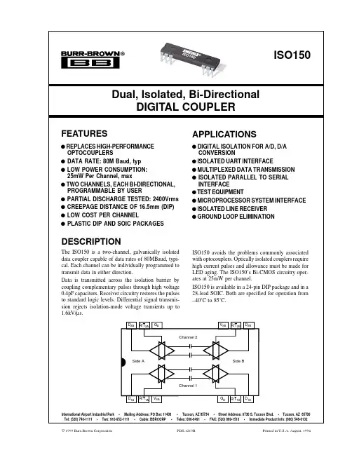
International Airport Industrial Park • Mailing Address: PO Box 11400 •Tucson, AZ 85734 • Street Address: 6730 S. Tucson Blvd. • Tucson, AZ 85706 Tel: (520) 746-1111 • Twx: 910-952-1111 • Cable: BBRCORP • Telex: 066-6491 • FAX: (520) 889-1510 • Immediate Product Info: (800) 548-6132© 1993 Burr-Brown Corporation PDS-1213B Printed in U.S.A. August, 19942®ISO150The information provided herein is believed to be reliable; however, BURR-BROWN assumes no responsibility for inaccuracies or omissions. BURR-BROWN assumes no responsibility for the use of this information, and all use of such information shall be entirely at the user’s own risk. Prices and specifications are subject to change without notice. No patent rights or licenses to any of the circuits described herein are implied or granted to any third party. BURR-BROWN does not authorize or warrant any BURR-BROWN product for use in life support devices and/or systems.SPECIFICATIONST A = +25°C, V S = +5V unless otherwise noted.ISO150AP, AUNOTES: (1) All devices receive a 1s test. Failure criterion is ≥5 pulses of ≥5pC. (2) The voltage rate-of-change across the isolation barrier that can be sustained without data errors. (3) Logic inputs are HCT-type and thresholds are a function of power supply voltage with approximately 0.4V hystersis—see text. (4) Supply current measured with both tranceivers set for the indicated mode. Supply current varies with data rate—see typical curves. (5) Calculated from the maximum Pulse Width Distortion (PWD), where Data Rate = 0.3/PWD. (6) Propagation time measured from V IN = 1.5V to V O = 2.5V. (7) The difference in propagation time of channel A and channel B in any combination of transmission directions. (8) The difference between progagation time of a rising edge and a falling edge.PARAMETERCONDITION MIN TYPMAXUNITS ISOLATION PARAMETERS Rated Voltage, Continuous 60Hz 1500Vrms Partial Discharge, 100% Test (1)1s, 5pC2400Vrms Creepage Distance (External)DIP—“P” Package 16mm SOIC—“U” Package 7.2mm Internal Isolation Distance0.10mm Isolation Voltage Transient Immunity (2) 1.6kV/µs Barrier Impedance >1014 || 7Ω || pF Leakage Current240Vrms, 60Hz 0.6µArms DC PARAMETERSLogic Output Voltage, High, V OHI OH = 6mA V S –1V S V Low, V OLI OL = 6mA 00.4V Logic Output Short-Circuit Current Source or Sink30mA Logic Input Voltage, High (3)2V S V Low (3)00.8V Logic Input Capacitance 5pF Logic Input Current<1nA Power Supply Voltage Range (3)35 5.5V Power Supply Current (4) Transmit Mode DC 0.001100µA 50MBaud 14mA Receive ModeDC 7.210mA 50MBaud 16mA AC PARAMETERS Data Rate, Maximum (5)C L = 50pF 5080MBaud Data Rate, Minimum DC Propagation Time (6)C L = 50pF 202740ns Propagation Delay Skew (7)C L = 50pF 0.52ns Pulse Width Distortion (8)C L = 50pF 1.56ns Output Rise/Fall Time, 10% to 90%C L = 50pF914ns Mode Switching Time Receive-to-Transmit 13ns Transmit-to-Receive 75ns TEMPERATURE RANGE Operating Range –4085°C Storage–40125°C Thermal Resistance,θJA75°C/W®3ISO150ABSOLUTE MAXIMUM RATINGSStorage Temperature .........................................................–40°C to +125°C Supply Voltages, V S ......................................................................–0.5 to 6V Transmitter Input Voltage, V I .............................................–0.5 to V S + 0.5V Receiver Output Voltage, V O .............................................–0.5 to V S + 0.5V R/T X Inputs.........................................................................–0.5 to V S + 0.5V Isolation Voltage dV/dt, V ISO ............................................................500kV/µs D X Short to Ground......................................................................Continuous Junction Temperature, T J ....................................................................175°C Lead Temperature (soldering, 10s).....................................................260°C 1.6mm below seating plane (DIP package).........................................300°CPACKAGE INFORMATION (1)PACKAGE DRAWINGMODEL PACKAGE NUMBERISO150AP 24-Pin Single-Wide DIP243-1ISO150AU28-Lead SOIC217-2NOTE: (1) For detailed drawing and dimension table, please see end of data sheet, or Appendix D of Burr-Brown IC Data Book.PIN CONFIGURATIONTOP VIEWDIP24 23 22 15 14 131 2 310 11 12D 1A R/T 1A V SA G B R/T 1B D 1B D 2A R/T 2A G A V SBR/T 2B D 2BPIN DESCRIPTIONSNAMEFUNCTIOND 1AData in or data out for transceiver 1A. R/T 1A held low makes D 1A an input pin.R/T 1A Receive/Transmit switch controlling transceiver 1A.V SA+5V supply pin for side A which powers transceivers 1A and 2A.G B Ground pin for transceivers 1B and 2B.R/T 1B Receive/Transmit switch controlling transceiver 1B.D 1B Data in or data out for transceiver 1B. R/T 1B held low makes D 1B an input pin.D 2B Data in or data out for transceiver 2B. R/T 2B held low makes D 2B an input pin.R/T 2B Receive/Transmit switch controlling D 2B .V SB +5V supply pin for side B which powers transceivers 1B and 2B.G A Ground pin for transceivers 1A and 2A.R/T 2A Receive/Transmit switch controlling transceiver 2A.D 2AData in or data out for transceiver 2A. R/T 2A held low makes D 2A in input pin.ELECTROSTATICDISCHARGE SENSITIVITYThis integrated circuit can be damaged by ESD. Burr-Brown recommends that all integrated circuits be handled with ap-propriate precautions. Failure to observe proper handling and installation procedures can cause damage.ESD damage can range from subtle performance degradation to complete device failure. Precision integrated circuits may be more susceptible to damage because very small parametric changes could cause the device not to meet its published specifications.4®ISO150TYPICAL PERFORMANCE CURVEST A = +25°C, V S = +5V unless otherwise noted.SUPPLY CURRENT PER CHANNELvs TEMPERATURETemperature (°C)–606 54 3 2 1–40–2020406080100120140S u p p l y C u r r e n t (m A)NORMALIZED RISE/FALL TIME vs TEMPERATURE1.61.51.41.31.21.11.0.9–60–40–2020406080100120140Temperature (°C)R e l a t i v e t r , t fSUPPLY CURRENT PER CHANNELvs SUPPLY VOLTAGE54321123456Supply Voltage, V S (V)S u p p l y C u r r e n t(m A )0POWER CONSUMPTION PER CHANNEL vs FREQUENCY Frequency (Hz)100k1M10M100MP o w e r (m W )S u p p l y C u r r e n t (m A )50 403020 100108642 0TYPICAL RISE AND FALL TIMES vs CAPACITIVE LOADvs SUPPLY VOLTAGE100806040200100200300400500Capacitive Load (pF)t r , t f (n s )PROPAGATION DELAY vs SUPPLY VOLTAGE4540353025202.53.0 3.54.0 4.55.0 5.5Supply Voltage, V S (V)P r o p a g a t i o n D e l a y (n s)®5ISO150TYPICAL PERFORMANCE CURVES (CONT)T A = +25°C, V S = +5V unless otherwise noted.ISOLATION VOLTAGE vs FREQUENCY10k 2.1k 1k1001011k10k100k1M10M100MFrequency (Hz)P e a k I s o l a t i o n V o l t a g e (V )PULSE WIDTH DISTORTIONvs TEMPERATURETemperature (°C)–605 4 3 2 1 0–40–2020406080100120140P u l s e W i d t h D i s t o r t i o n , P W D (n s)OUTPUT VOLTAGE vs LOGIC INPUT VOLTAGE5432100.5 1.0 1.5 2.0V IN (V)V O U T (V)PROPAGATION DELAY vs TEMPERATURE6050403020100–60–40–2020406080100120140Temperature (°C)P r o p a g a t i o n D e l a y , t P D (n s )LOGIC INPUT THRESHOLD VOLTAGEvs SUPPLY VOLTAGE2.01.81.61.41.21.00.80.60.40.202.02.53.03.54.04.55.05.56.0Supply Voltage, V SS (V)V I N (V)ISOLATION LEAKAGE CURRENT vs FREQUENCY100m10m1m 100µ10µ1µ100n1101001k 10k100k1MFrequency (Hz)L e a k a g e C u r r e n t (A r ms )6®ISO150TYPICAL PERFORMANCE CURVES (CONT)T A = +25°C, V S = +5V unless otherwise noted.ISOLATION BARRIERData is transmitted by coupling complementary logic pulses to the receiver through two 0.4pF capacitors. These capaci-tors are built into the ISO150 package with Faraday shield-ing to guard against false triggering by external electrostatic fields.The integrity of the isolation barrier of the ISO150 is verified by partial discharge testing. 2400Vrms, 60Hz, is applied across the barrier for one second while measuring any tiny discharge currents that may flow through the barrier. These current pulses are produced by localized ionization within the barrier. This is the most sensitive and reliable indicator of barrier integrity and longevity, and does not damage the barrier. A device fails the test if five or more current pulses of 5pC or greater are detected.FIGURE 1. Basic Operation Diagram.Conventional isolation barrier testing applies test voltage far in excess of the rated voltage to catastrophically break down a marginal device. A device that passes the test may be weakened, and lead to premature failure.APPLICATIONS INFORMATIONFigure 1 shows the ISO150 connected for basic operation.Channel 1 is configured to transmit data from side B to A.Channel 2 is set for transmission from side A to B. The R/T pins for each of the four transceivers are shown connected to the required logic level for the transmission direction shown. The transmission direction can be controlled by logic signals applied to the R/T pins. Channel 1 and 2 can be independently controlled for the desired transmission direction.TYPICAL INSULATION RESISTANCE vs TEMPERATURE 101610151014101310121011101020406080100120140160180Temperature (°C)I s o l a t i o n R e s i s t a n c e (Ω)®7ISO150LOGIC LEVELSA single pin serves as a data input or output, depending on the mode selected. Logic inputs are CMOS with thresholds set for TTL compatibility. The logic threshold is approxi-mately 1.3V with 5V supplies and with approximately 400mV of hysteresis. Input logic thresholds vary with the power supply voltage. Drive the logic inputs with signals that swing the full logic voltage swing. The ISO150 will use somewhat greater quiescent current if logic inputs do not swing within 0.5V of the power supply rails.In receive mode, the data output can drive 15 standard LS-TTL loads. It will also drive CMOS loads. The output drive circuits are CMOS.POWER SUPPLYSeparate, isolated power supplies must be connected to side A and side B to provide galvanic isolation. Nominal rated supply voltage is 5V. Operation extends from 3V to 5.5V.Power supplies should be bypassed close to the device pins on both sides of the isolation barrier.The V S pin for each side powers the transceivers for both channel 1 and 2. The specified supply current is the total of both transceivers on one side, both operating in the indicated mode. Supply current for one transceiver in transmit mode and one in receive mode can be estimated by averaging the specifications for transmit and receive operation. Supply current varies with the data transmission rate—see typical curves.POWER-UP STATEThe ISO150 transmits information across the barrier only when the input-side data changes logic state. When a trans-ceiver is first programmed for receive mode, or is powered-up in receive mode, its output is initialized “high”. Subse-quent changes of data applied to the input side will cause the output to properly reflect the input side data.SIGNAL LOSSThe ISO150’s differential-mode signal transmission and careful receiver design make it highly immune to voltage across the isolation barrier (isolation-mode voltage). Rapidly changing isolation-mode voltage can cause data errors. As the rate of change of isolation voltage is increased, there is a very sudden increase in data errors. Approximately 50% of ISO150s will begin to produce data errors with isolation-mode transients of 1.6kV/µs. This may occur as low as 500V/µs in some devices. In comparison, a 1000Vrms, 60Hz isolation-mode voltage has a rate of change of approximately 0.5V/µs.Still, some applications with large, noisy isolation-mode voltage can produce data errors by causing the receiver output to change states. After a data error, subsequent changes in input data will produce correct output data.PROPAGATION DELAY AND SKEWLogic transitions are delayed approximately 27ns through the ISO150. Some applications are sensitive to data skew—the difference in propagation delay between channel 1 and channel 2. Skew is less than 2ns between channel 1 and channel 2. Applications using more than one ISO150 must allow for somewhat greater skew from device to device.Since all devices are tested for delay times of 20ns min to 40ns max, 20ns is the largest device-to-device data skew.MODE CHANGESThe transmission direction of a channel can be changed “on the fly” by reversing the logic levels at the channel’s R/T pins on both side A and side B. Approximately 75ns after the transceiver is programmed to receive mode its output is initialized “high”, and will respond to subsequent input-side changes in data.STANDBY MODEQuiescent current of each transceiver circuit is very low in transmit mode when input data is not changing (1nA typi-cal). To conserve power when data transmission is not required, program both side A and B transceivers for trans-mit mode. Input data applied to either transceiver is ignored by the other side. High speed data applied to either trans-ceiver will increase quiescent current.CIRCUIT LAYOUTThe high speed of the ISO150 and its isolation barrier require careful circuit layout. Use good high speed logic layout techniques for the input and output data lines. Power supplies should be bypassed close to the device pins on both sides of the isolation barrier. Use low inductance connec-tions. Ground planes are recommended.Maintain spacing between side 1 and side 2 circuitry equal or greater than the spacing between the missing pins of the ISO150 (approximately 16mm for the DIP version). Sockets are not recommended.8®ISO150FIGURE 2. Isolated RS-485 Interface.®9ISO150F IG U R E 3. I S O 150 a n d A D S 7807 i s U s e d t o R e d u c e C i r c u i t N o i s e i n a M i x e d S i g n a l A p p l i c a t i o n .元器件交易网。
2N5551中文资料(fairchild)中文数据手册「EasyDatasheet - 矽搜」
50 VCB = 100V
10
10
10
1β
100 Co
o
125 C
0.1
o
-40 Co
25 Co
75 C
- CCEO(SALT)LECTOR-EMITTER VOLTAGE [V]
0.01
V
1
10
100
IC- COLLECTOR CURRENT [mA]
Figure 2. Collector-Emitter Saturation Voltage vs.
芯片中文手册,看全文,戳
2N5551 / MMBT5551 NPN通用放大器
2013年6月
描写
该装置是专为通用高压放大器和气体放电的显示驱动程序.
2N5551
TO-92
MMBT5551
3
2
1 SOT-23
Marking: 3S 1. Base 2. Emitter 3. Collector
MMBT5551
350 2.8
357
Units
mW mW/°C °C/W °C/W
2
芯片中文手册,看全文,戳
电气特性
(4)
价值观是在T 符
A = 25°C除非另有说明. 参数
断特性
V(BR)CEO 集电极 - 发射极击穿电压 V(BR)CBO 集电极基击穿电压 V (BR)EBO 发射极基极击穿电压
Value
160 180
6 600 -55到+150
2N5551 / MMBT5551 - NPN通用放大
器
Units
V V V mA °C
热特性
价值观是在T
2SC3423中文资料(toshiba)中文数据手册「EasyDatasheet - 矽搜」
电气特性
(Tc = 25°C)
特点
符号
பைடு நூலகம்
测试条件
集电极截止电流 发射极截止电流
DC电流增益
集电极 - 发射极饱和电压 基极 - 发射极电压
转换频率 集电极输出电容
ICBO
VCB = 150 V, I E = 0
IEBO
VEB = 5 V, I C = 0
hFE VCE = 5 V, I C =10毫安
1000
(MHz) 500 300
T
Common emitter Tc = 25°C
100
Transitio5n0 frequency f 30
fT – IC
VCE = 10 V 5
10
0.5 1
3
10
30
100
Collector current I C (mA)
1000 500 FE 300
100 50 DC current gain h 30
温度等)可能会导致该产品在可靠性降低显著即使操作条件
重量:1.3克(典型值).
(即
工作温度/电流/电压等)在绝对最大额定值范围内.
请在审查东芝半导体可靠性手册("注意事项"/降级概念和方法)和个人可靠性数据(即可靠性试
验报告,并估计故障率等)设计适当可靠性.
1
2006-11-09
芯片中文手册,看全文,戳
集光力 耗散
Ta = 25°C Tc = 25°C
VCBO VCEO VEBO
IC IB
PC
150
V
150
V
5
V
50
mA
5
mA
2SK4145中文资料(NEC)中文数据手册「EasyDatasheet - 矽搜」
数据表
交换
N沟道功率MOS FET
2SK4145
描述 2SK4145是N沟道MOS场效应晶体管设计用于高电流开关应用.
特征
低通态电阻
R = 10mΩ以下. (V
低输入电容
C = 5300 pF TYP.
= 10 V, I = 42 A)
订购信息
零件号
镀铅
2SK4145-S19-AY
75 100 125 150 175
T - 外壳温度 -
°C
正向偏置安全工作区
1000
100
10
I
漏极电流
-1一个
0.1
0.1
1
10
100
V - 漏极至源极电压 - V
1000 °C/ W
瞬态热电阻与脉冲宽度
100
总功耗对比 外壳温度
100
80
60
40
20 - 总功耗 - W P
0
0
25 50 75 100 125 150 175
R
-75 -25 25 75
T - 通道温度 -
脉冲
125 175 °C
1000
开关特性
100
t
t
- 开关时间 - 纳秒t , t 10
,t
V = 30 V
,t
V = 10 V
t
R =0
1
0.1
1
t
10
100
I - 漏极电流 - 一个
1000
源极到漏极二极管 正向电压
100
V = 10 V
0V
10
1
250
200 150
电子元器件zvnl120a中文资料_数据手册_IC数据表
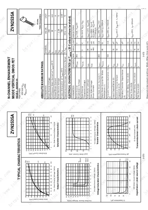
ZVN2535A
TYPICAL CHARACTERISTICS
800
VGS=
10V
700
6V
600
500
400
4V
300
200 3V
100
0 0 10 20 30 40 50 60 70 80 90 100
VDS - Drain Source Voltage (Volts)
Output Characteristics
Gate-Body Leakage
Zero Gate Voltage Drain Current
IGSS IDSS
20
nA VGS=± 20V, VDS=0V
10
µA VDS=350V, VGS=0
400 µA VDS=280V, VGS=0V,
T=125°C(2)
On-State Drain Current(1)
Input Capacitance (2)
Common Source Output Capacitance (2)
gfs-Transconductance (mS)
250 200 150 100
50
0
0
100
200
300
400
500
ID- Drain Current (mA)
Transconductance v drain current
3-373
N-CHANNEL ENHANCEMENT
MODE VERTICAL DMOS FET
ISSUE 2 – MARCH 94 FEATURES * 350 Volt VDS
RDS(on)=35Ω
ZVN2535A
VDRP-240-48中文资料
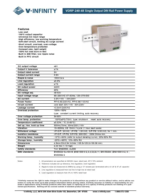
DC output voltage48V Output V.tolerance±1%Output rated current5A Output current range0-5A Ripple & noise150mVp-p Line regulation±0.5%Load regulation±1% DC output power240W Efficiency85% DC voltage adj.48-53V Input voltage range85~264VAC 47~63Hz; 120~370VDC AC current3.5A/115V 1.8A/230V Power FactorPF>0.95/230VAC, PF>0.98/115VAC Inrush currentcold start 30A/115V 50A/230V Leakage current<3.5mA/240VAC Overload protection105%~150%type: constant current limiting, auto recovery Over voltage protection54-60V Over temp. protection100ºC±5ºC(TSW) type: shutdown reset: auto recovery Temperature coefficient±0.03% / °C (0~50°C)Set up, rise, hold up time500ms;70ms; 30ms/230V,115V Vibration10~500Hz, 2G 10min./1cycle (1 hour each axes)Withstand voltageI/P-O/P: 3KVAC, I/P-FG: 1.5KVAC, O/P-FG: 0.5KVAC, for 1 min.Isolation resistanceI/P-O/P, I/P-FG, O/P-FG: 500VDC / 100M Ohms min.Working temp., humidity-10°C~+60% (refer to output derating curve), 20%-90% RH Storage temp., humidity-20ºC~+85ºC, 10%~95% RH Dimensions4.94x4.93x3.94 inches (125.5x125.2x100.08 mm) Weight2.43 lbs (1.10 Kgs) Safety standardsTUV EN60950, UL508EMC standards EN55022 CLASS B ,EN61000-4-2,3,4,5,6,8,11; ENV50204 ,EN61000-3-2,-3 ,EN50082-2Notes: 1. All parameters are specified at 230VAC input, rated load, 25°C 70% ambient2. Tolerance includes set up tolerance, line regulation, load regulation3. Ripple & noise are measured at 20MHz by using a 12” twisted pair terminated with a 0.1uF & 47 uF capacitor4. Line regulation is measured from low line to high line at rated load5, Load regulation is measure from 0% to 100% rated load*V-Infinity reserves the right to make changes to its products or to discontinue any product or service without notice, and to advise cus-tomers to verify the most up-to-date product information before placing orders. V-Infinity assumes no liability or responsibility for cus-tomer’s applications using V-Infinity products other than repair or replacing (at V-I’s option) V-Infinity products not meeting V-I’s pub-lished specifications. Nothing will be covered outside of standard product warranty.Features·Low cost·105°C output capacitor·Universal AC input range·High efficiency, low working temperature·Soft-start circuit, limiting AC surge current·Short circuit, overload, over-voltage·Over-temperature protected·Compact size, light weight·100% full load burn-in test·Built in EMI filter, low ripple noise·Built in PFC circuitDimensions (mm)。
4051中文资料
4051CMOS ICMULTIPLEXERS/DEMULTIPLEXERSDESCRIPTIONUTC 4051 is single 8-channel analog multiplexers/demultiplexersfor application as digitally–controlled analog switches.The device has three binary control inputs and an inhibit input. Itfeature low ON impedance and very low OFF leakage current.Control of analog signals up to the complete supply voltage rangecan be achieved.FEATURES* Wide Analog Voltage Range: V DD–V EE = 3V~18V.(Note: V EE must be V SS)*Pb-free plating product number: 4051L * Break-Before-Make Switching Eliminates Channel Overlap.* Linearized Transfer Characteristics* Implement an SP8T solid state switch effectively.* Pin–to–Pin Replacement for CD4051ORDERING INFORMATIONOrder NumberPackage PackingNormal Lead Free PlatingReel4051-S16-R 4051L-S16-R SOP-16 Tape4051-S16-T 4051L-S16-T SOP-16 TubeTSSOP-16TapeReel4051-P16-R 4051L-P16-RTSSOP-16Tube4051-P16-T 4051L-P16-T4051-D16-T 4051L-D16-T DIP-16 TubePIN CONFIGURATION1 2 3 4 5 6 7 8161514131211109X1V DDX2ABC UTC 4051X4 X6 XX7 X5 INH V EE V SS X0 X3PIN DESCRIPTIONPIN No. SYMBAL NAME AND FUNCTION3 XCommonInput/Output6 INHInhibitInputs7 V EE SupplyVoltage8 V SS Ground11,10,9 A,B,CBinary Control Inputs13,14,15,12,1,5,2,4 X0~X7 IndependentInputs/Outputs16 V DD Positive Supply VoltageABSOLUTE MAXIMUM RATINGPARAMETER SYMBOL RATINGS UNITDC Supply Voltage (Referenced to V EE , V SS V EE ) V DD -0.5 ~ +18 V Input or Output Voltage (DC or Transient)(Referenced to V SS for Control Inputs and V EE for Switch I/O) V IN , V OUT -0.5 ~ V DD +0.5 VInput Current (DC or Transient), per Control Pin I IN ±10 mA Switch Through Current I SW ±25 mAPower Dissipation Derating above 65℃ P D 500 7mW mW/℃ Junction Temperature T J 125 ℃ Operating Temperature Range T OPR -40 ~ +125℃ Storage Temperature Range T STG -40 ~ +150℃ Note: 1.Absolute maximum ratings are those values beyond which the device could be permanently damaged.Absolute maximum ratings are stress ratings only and functional device operation is not implied.2.The device is guaranteed to meet performance specification within 0 ~70 operating temperature range and assured by design from –40 ~125 . ELECTRICAL CHARACTERISTICS (Ta=25 , unless otherwise specified.)PARAMETER SYMBOL TEST CONDITIONS MIN TYP MAX UNITSUPPLY REQUIREMENTS (Voltages Referenced to V EE )Power Supply Voltage Range V DD V DD – 3.0 V SS V EE3 18 V V DD =5V 0.005 5 V DD =10V 0.010 10Quiescent Current perPackageV DD =15V I Q Control Inputs: V IN = V SS or V DDSwitch I/O: V EE V I/O V DD , and ∆Vsw 500mV(Note 2) 0.015 20 µA V DD =5V (0.07 µA/kHz) f + I Q V DD =10V (0.20 µA/kHz) f + I Q Total Supply Current(Dynamic Plus Quiescent, Per Package) V DD =15VI D(AV) T a =25 only (The channel component, (V IN -Vout)/Ron, is not included.) (0.36 µA/kHz) f + I Q µASWITCHES IN/OUT AND COMMONS OUT/IN -- X, Y, Z (Voltages Referenced to V EE ) Recommended Peak–to–PeakVoltage Into or Out of the Switch V I/O Channel On or Off 0 V DD V PPRecommended Static or DynamicVoltage Across the Switch ∆Vsw Channel On 0 600 mVOutput Offset Voltage V O(OFF)V IN = 0V, No Load 10 µVV DD =5V 250 1050V DD =10V 120 500ON Resistance V DD =15V R ON ∆Vsw 500mV V IN = V IL or V IH (Control), and V IN = 0 to V DD (Switch) 80 280Ω V DD =5V 25 70V DD =10V 10 50ON Resistance Between Any Two Channels in the Same Package V DD =15V∆R ON 10 45 Ω Off–Channel Leakage Current I OFF V IN = V IL or V IH (Control)Channel to Channel or AnyOne Channel, V DD =15V±0.05 ±100 nA Capacitance, Switch I/O C I/O Inhibit = V DD 10 pF Capacitance, Common O/I C O/I Inhibit = V DD 17 pFCapacitance, Feedthrough(Channel Off)C I/OPins Not Adjacent Pins Adjacent 0.15 0.47 pFELECTRICAL CHARACTERISTICS(Cont.)PARAMETER SYMBOL TEST CONDITIONS MIN TYP MAX UNITCONTROL INPUTS – INHIBIT A, B, C (Voltages Referenced to V SS )V DD =5V 2.25 1.5V DD =10V 4.50 3.0Low Level Input Voltage V DD =15V V IL R ON = per spec, I OFF = per spec 6.75 4.0 V V DD =5V 3.5 2.75V DD =10V 7 5.5High Level Input Voltage V DD =15V V IH R ON = per spec, I OFF = per spec 11 8.25V Input Leakage Current I LEAK V IN = 0 or V DD , V DD =15V ±0.00001 ±0.1µA Input Capacitance C IN 5.0 7.5 pFDYNAMIC ELECTRICAL CHARACTERISTICS(C L = 50pF, T a =25 , V EE V SS , unless otherwise specified)PARAMETER SYMBOLV DD –V EEVdcTEST CONDITIONS MIN TYP MAX UNIT Propagation Delay Times Switch Input to Switch Output (R L = 10 k Ω) t PLH, t PHL510 15 t PLH , t PHL =(0.17 ns/pF)C L + 26.5ns t PLH , t PHL =(0.08 ns/pF)C L + 11ns t PLH , t PHL =(0.06 ns/pF)C L + 9ns35 15 12 90 40 30 ns Inhibit to Outputt PHZ, t PLZt PZH, t PZL510 15 (R L =10k Ω, V EE =V SS ) Output “1” or “0” to High Impedance, or High Impedance to “1” or “0” Level350 170 140 700340280ns Control Input to Output t PLH, t PHL 510 15 R L = 10 k Ω, V EE = V SS360 160 120 720320240ns Total Harmonic Distortion THD 10 R L = 10K Ω, f = 1 kHz, Vin = 5 V PP 0.07 %Bandwidth BW 10 R L = 1k Ω, V IN = 1/2 (V DD –V EE ) p–p, C L = 50pF, 20 Log (Vout/Vin) = -3dB)17 MHzOff Channel Feedthrough Attenuation 10 R L =1K Ω, V IN = 1/2 (V DD –V EE ) p–p f IN = 4.5 MHz-50 dBChannel Separation 10 R L = 1k Ω, V IN = 1/2 (V DD –V EE ) p–p f IN = 3MHz-50 dBCrosstalk, Control Input to Common O/I 10 R 1 = 1k Ω, R L = 10k Ω Control t TLH = t THL = 20ns, Inhibit = V SS75 mVNote 1. Data of “TYP” is intended as an indication of the IC’s potential performance.2. For voltage drops across the switch(∆Vsw)>600mV (>300mV at high temperature), excessive V DD current may be drawn, i.e. the current out of the switch may contain both V DD and switch input components. The reliability of the device will be unaffected unless the Maximum Ratings are exceeded.TEST CIRCUITSwitch Circuit SchematicTRUTH TABLEControl InputsINHIBIT C B AON Switches0 0 0 0 0 0 0 0 0 1 0 1 0 0 1 1 X0 X1 X2 X3 0 0 0 01 0 0 1 0 1 1 1 0 1 1 1X4 X5 X6 X7 1 x x x Nonex = Don’t Care9B 1C A 6INH X4 1X5 5X6 2X7 43XUTC 4051Functional DiagramTYPICAL CHARACTERISTICSInput Voltage, V IN (V)Input Voltage , V IN (V )"O N " R e s i s ta n c e , R O N300350200Input Voltage , V IN (V)"O N " R e s i s t a n c e , R O N( )25015010050。
LM2590HV-AQ中文资料
LM2590HV-AQSIMPLE SWITCHER ®Power Converter 150kHz 1A Step-Down Voltage Regulator,with FeaturesGeneral DescriptionThe LM2590HV-AQ regulator is a monolithic integrated cir-cuit which provides all the active functions for a step-down (buck)switching regulator,and is capable of driving a 1Amp load with excellent line and load regulation.The LM2590HV-AQ is available in fixed output voltages of 3.3V,5.0V,as well as an adjustable output version.The LM2590HV-AQ switching regulator is similar to the LM2591HV with additional supervisory and performance fea-tures.Requiring a minimum number of external components,these regulators are simple to use and include internal frequency compensation †,improved line and load specifications,fixed-frequency oscillator,Shutdown/Soft-start,output error flag and flag delay.The LM2590HV-AQ operates at a switching frequency of 150kHz thus allowing smaller sized filter components than what would be needed with lower frequency switching regu-lators.Available in a standard 7-lead TO-220package with several different lead bend options,and a 7-lead TO-263Surface mount package.Other features include a guaranteed ±4%tolerance on out-put voltage under all conditions of input voltage and output load conditions,and ±15%on the oscillator frequency.Ex-ternal shutdown is included,featuring typically 90µA standby current.Self protection features include a two stage current limit for the output switch and an over temperature shutdown for complete protection under fault conditions.Featuresn Reliability Qualification for Automotive n 3.3V,5V,and adjustable output versionsn Adjustable version output voltage range,1.2V to 57V ±4%max over line and load conditions n Guaranteed 1A output load currentn Available in 7-pin TO-220and TO-263(surface mount)Packagen Input voltage range up to 60Vn 150kHz fixed frequency internal oscillator n Shutdown/Soft-startn Out of regulation error flag n Error flag delayn Low power standby mode,I Q typically 90µA n High Efficiencyn Thermal shutdown and current limit protectionApplicationsn Simple high-efficiency step-down (buck)regulator n Efficient pre-regulator for linear regulators n On-card switching regulators nPositive to Negative converterNote:†Patent Number 5,382,918.Typical Application(Fixed Output Voltage Versions)20097101SIMPLE SWITCHER ®and Switchers Made Simple ®are registered trademarks of National Semiconductor Corporation.May 2004LM2590HV-AQ SIMPLE SWITCHER Power Converter 150kHz 1A Step-Down Voltage Regulator,with Features©2004National Semiconductor Corporation Absolute Maximum Ratings (Note 1)If Military/Aerospace specified devices are required,please contact the National Semiconductor Sales Office/Distributors for availability and specifications.Maximum Supply Voltage (V IN )63V SD /SS Pin Input Voltage (Note 2)6V Delay Pin Voltage (Note 2) 1.5VFlag Pin Voltage −0.3≤V ≤45V Feedback Pin Voltage −0.3≤V ≤+25VOutput Voltage to Ground (Steady State)−1VPower DissipationInternally limited Storage Temperature Range −65˚C to +150˚CESD Susceptibility (Note 3)Human Body Model (AEC-100-002)2kV Machine Model (AEC-100-003)200VLead Temperature S PackageVapor Phase (60sec.)+215˚C Infrared (10sec.)+245˚C T Package (Soldering,10sec.)+260˚C Maximum Junction Temperature+150˚COperating ConditionsAmbient Temperature Range −40˚C ≤T A ≤+125˚C Junction Temperature Range −40˚C ≤T J ≤+150˚C Supply Voltage+4.5V ≤V IN ≤+60VLM2590HV-3.3-AQ Electrical CharacteristicsSpecifications with standard type face are for T J =25˚C,and those with boldface type apply over full Operating Tempera-ture Range.SymbolParameterConditionsLM2590HV-3.3-AQUnitsMin Typ Max (Note 5)(Note 4)(Note 5)SYSTEM PARAMETERS (Note 6)Test Circuit Figure 1V OUT Output Voltage 4.75V ≤V IN ≤60V,0.2A ≤I LOAD ≤1A 3.1683.1353.3 3.4323.465V V ηEfficiencyV IN =12V,I LOAD =1A77%LM2590HV-5.0-AQ Electrical CharacteristicsSpecifications with standard type face are for T J =25˚C,and those with boldface type apply over full Operating Tempera-ture Range.SymbolParameterConditionsLM2590HV-5.0-AQ UnitsMin Typ Maxt (Note 5)(Note 4)(Note 5)SYSTEM PARAMETERS (Note 6)Test Circuit Figure 1V OUT Output Voltage 7V ≤V IN ≤60V,0.2A ≤I LOAD ≤1A 4.8004.7505 5.2005.250V V ηEfficiencyV IN =12V,I LOAD =1A82%LM2590HV-ADJ-AQ Electrical CharacteristicsSpecifications with standard type face are for T J =25˚C,and those with boldface type apply over full Operating Tempera-ture Range.SymbolParameterConditionsLM2590HV-ADJ-AQ UnitsMin Typ Max (Note 5)(Note 4)(Note 5)SYSTEM PARAMETERS (Note 6)Test Circuit Figure 1V FB Feedback Voltage 4.5V ≤V IN ≤60V,0.2A ≤I LOAD ≤1A 1.1931.1801.230 1.2671.280V V I FB Feedback Bias Current V FB =1.30V1050300nA nA ηEfficiencyV IN =12V,V OUT =3V,I LOAD =1A76%L M 2590H V -A Q 2All Output Voltage VersionsElectrical CharacteristicsSpecifications with standard type face are for T J=25˚C,and those with boldface type apply over full Operating Tempera-ture Range.Unless otherwise specified,V IN=12V for the3.3V,5V,and Adjustable version.I LOAD=500mASymbol Parameter Conditions LM2590HV-XXX-AQUnitsMin Typ Max(Note5)(Note4)(Note5)DEVICE PARAMETERSf O OscillatorFrequency (Note7)127110150173173kHzkHzV SAT Saturation Voltage I OUT=1A(Note8)(Note9)0.95 1.21.3V VDC Max Duty Cycle(ON)(Note9)100%Min Duty Cycle(OFF)(Note10)0%I CLIM Switch currentLimit Peak Current,(Note8)(Note9) 1.31.21.92.83.0AAI L Output LeakageCurrentOutput=0V(Note8)(Note10)Note11)50µAOutput=−1V(Note8)(Note10)Note11)530mAI Q OperatingQuiescent CurrentSD/SS Pin Open(Note10)510mAI STBY Standby QuiescentCurrent SD/SS pin=0V(Note11)90200250µAµAθJC ThermalResistanceTO220or TO263Package,Junction to Case2˚C/W θJA TO220Package,Junction to Ambient(Note12)50˚C/W θJA TO263Package,Junction to Ambient(Note13)50˚C/W θJA TO263Package,Junction to Ambient(Note14)30˚C/W θJA TO263Package,Junction to Ambient(Note15)20˚C/W SHUTDOWN/SOFT-START CONTROL Test Circuit of Figure1V SD ShutdownThreshold VoltageShutdown Mode,I STBY<250µA0.6 1.3 2.0VV OUT=1%of Normal Output Voltage 1.8VV SS Soft-start Voltage V OUT=20%of Nominal Output Voltage2VV OUT=100%of Nominal Output Voltage3VI SD Shutdown Current V SHUTDOWN=0.5V510µAI SS Soft-start Current V Soft-start=2.5V 1.55µALM2590HV-AQ3All Output Voltage VersionsElectrical Characteristics (Continued)Specifications with standard type face are for T J =25˚C,and those with boldface type apply over full Operating Tempera-ture Range .Unless otherwise specified,V IN =12V for the 3.3V,5V,and Adjustable version.I LOAD =500mA SymbolParameterConditionsLM2590HV-XXX-AQUnitsMin Typ Max (Note 5)(Note 4)(Note 5)FLAG/DELAY CONTROL Test Circuit of Figure 1Regulator Dropout Detector Threshold VoltageLow (Flag ON)929698%VF SAT Flag OutputSaturation Voltage I SINK =3mA V DELAY =0.5V 0.30.71.0V IF L Flag OutputLeakage Current V FLAG =60V 0.3µAVD THDelay PinThreshold VoltageV OUT Regulated 1.21 1.25 1.29V I DELAY Delay Pin SourceCurrent V DELAY =0.5V 36µA ID SAT Delay PinSaturationLow (Flag ON)70350400mV mVNote 1:Absolute Maximum Ratings indicate limits beyond which damage to the device may occur.Operating Ratings indicate conditions for which the device is intended to be functional,but do not guarantee specific performance limits.For guaranteed specifications and test conditions,see the Electrical Characteristics.Note 2:Voltage internally clamped.If clamp voltage is exceeded,limit current to a maximum of 1mA.Note 3:The human body model is a 100pF capacitor discharged through a 1.5k resistor;the Machine Model is 200pF discharged through a 0Ωresistor.Note 4:Typical numbers are at 25˚C and represent the most likely norm.Note 5:All limits guaranteed at room temperature (standard type face)and at temperature extremes (bold type face).All room temperature limits are 100%production tested.All limits at temperature extremes are guaranteed via correlation using standard Statistical Quality Control (SQC)methods.All limits are used to calculate Average Outgoing Quality Level (AOQL).Note 6:External components such as the catch diode,inductor,input and output capacitors can affect switching regulator system performance.When the LM2590HV-AQ is used as shown in the Figure 1test circuit,system performance will be as shown in system parameters section of Electrical Characteristics.Note 7:The switching frequency is reduced when the second stage current limit is activated.The amount of reduction is determined by the severity of current overload.Note 8:No diode,inductor or capacitor connected to output pin.Note 9:Feedback pin removed from output and connected to 0V to force the output transistor switch ON.Note 10:Feedback pin removed from output and connected to 12V for the 3.3V,5V,and the ADJ.version to force the output transistor switch OFF.Note 11:V IN =60V.Note 12:Junction to ambient thermal resistance (no external heat sink)for the package mounted TO-220package mounted vertically,with the leads soldered to a printed circuit board with (1oz.)copper area of approximately 1in 2.Note 13:Junction to ambient thermal resistance with the TO-263package tab soldered to a single sided printed circuit board with 0.5in 2of (1oz.)copper area.Note 14:Junction to ambient thermal resistance with the TO-263package tab soldered to a single sided printed circuit board with 2.5in 2of (1oz.)copper area.Note 15:Junction to ambient thermal resistance with the TO-263package tab soldered to a double sided printed circuit board with 3in 2of (1oz.)copper area on the LM2590HVS-AQ side of the board,and approximately 16in 2of copper on the other side of the p-c board.See application hints in this data sheet and the thermal model in Switchers Made Simple available at .L M 2590H V -A Q 4Typical Performance Characteristics(Circuit of Figure 1)NormalizedOutput VoltageLine Regulation20097183200971A0Efficiency Switch SaturationVoltage2009718520097186Switch Current Limit Dropout Voltage200971A2200971A3LM2590HV-AQ5Typical Performance Characteristics (Circuit of Figure 1)(Continued)OperatingQuiescent CurrentShutdown Quiescent Current200971A4200971A5Minimum Operating Supply VoltageFeedback Pin Bias Current200971A6200971A7Flag Saturation Voltage Switching Frequency200971A8200971A9L M 2590H V -A Q 6Typical Performance Characteristics(Circuit of Figure1)(Continued)Soft-startShutdown/Soft-startCurrent200971B0200971B1Delay Pin Current Soft-start Response200971B220097118Shutdown/Soft-startThreshold Voltage Internal Gain-Phase Characteristics200971A120097178LM2590HV-AQ7Typical Performance Characteristics(Circuit of Figure1)(Continued)Continuous Mode Switching WaveformsV IN=20V,V OUT=5V,I LOAD=1AL=52µH,C OUT=100µF,C OUT ESR=100mΩDiscontinuous Mode Switching WaveformsV IN=20V,V OUT=5V,I LOAD=250mAL=15µH,C OUT=150µF,C OUT ESR=90mΩ20097120A:Output Pin Voltage,10V/div.B:Inductor Current0.5A/div.C:Output Ripple Voltage,50mV/div.Horizontal Time Base:2µs/div.20097119A:Output Pin Voltage,10V/div.B:Inductor Current0.25A/div.C:Output Ripple Voltage,100mV/div.Horizontal Time Base:2µs/div.Load Transient Response for Continuous ModeV IN=20V,V OUT=5V,I LOAD=250mA to1AL=52µH,C OUT=100µF,C OUT ESR=100mΩLoad Transient Response for Discontinuous ModeV IN=20V,V OUT=5V,I LOAD=250mA to1AL=15µH,C OUT=150µF,C OUT ESR=90mΩ20097121A:Output Voltage,100mV/div.(AC)B:250mA to1A Load PulseHorizontal Time Base:50µs/div.20097122A:Output Voltage,100mV/div.(AC)B:250mA to1A Load PulseHorizontal Time Base:200µs/div.LM259HV-AQ8Connection Diagrams and Order InformationBent and Staggered Leads,Through Hole Package7-Lead TO-220(T)Surface Mount Package 7-Lead TO-263(S)20097150See NS Package Number TA07B 20097123See NS Package Number TS7BORDER INFORMATIONTO-220TO-263Adjustable LM2590HVTADJ-AQ LM2590HVSADJ-AQ 3.3V LM2590HVT3.3-AQ LM2590HVS3.3-AQ 5.0VLM2590HVT5.0-AQLM2590HVS5.0-AQLM2590HV-AQ9Test Circuit and Layout GuidelinesFixed Output Voltage Versions20097124Component Values shown are for V IN =15V,V OUT =5V,I LOAD =1A.C IN —470µF,50V,Aluminum Electrolytic Nichicon “PM Series”C OUT —220µF,25V Aluminum Electrolytic,Nichicon “PM Series”D1—2A,60V Schottky Rectifier,21DQ06(International Rectifier)L1—68µH,See Inductor Selection ProcedureAdjustable Output Voltage Versions20097125Select R 1to be approximately 1k Ω,use a 1%resistor for best ponent Values shown are for V IN =20V,V OUT =10V,I LOAD =1A.C IN :—470µF,35V,Aluminum Electrolytic Nichicon “PM Series”C OUT :—220µF,35V Aluminum Electrolytic,Nichicon “PM Series”D1—2A,60V Schottky Rectifier,21DQ06(International Rectifier)L1—100µH,See Inductor Selection Procedure R 1—1k Ω,1%R 2—7.15k,1%C FF —3.3nF Typical Values C SS —0.1µF C DELAY —0.1µFR PULL UP —4.7k (use 22k if V OUT is ≥45V)†Resistive divider is required to aviod exceeding maximum rating of 45V/3mA on/into flag pin.††Small signal Schottky diode to prevent damage to feedback pin by negative spike when output is shorted (C FF not being able to discharge immediately willdrag feedback pin below ground).Required if V IN >40VFIGURE 1.Standard Test Circuits and Layout GuidesL M 2590H V -A Q 10Block Diagram20097130Pin Functions+V IN(Pin1)—This is the positive input supply for the IC switching regulator.A suitable input bypass capacitor must be present at this pin to minimize voltage transients and to supply the switching currents needed by the regulator. Output(Pin2)—Internal switch.The voltage at this pin switches between approximately(+V IN−V SAT)and approxi-mately−0.5V,with a duty cycle of V OUT/V IN.Error Flag(Pin3)—Open collector output that goes active low(≤1.0V)when the output of the switching regulator is out of regulation(less than95%of its nominal value).In this state it can sink maximum3mA.When not low,it can be pulled high to signal that the output of the regulator is in regulation(power good).During power-up,it can be pro-grammed to go high after a certain delay as set by the Delay pin(Pin5).The maximum rating of this pin should not be exceeded,so if the rail to which it will be pulled-up to is higher than45V,a resistive divider must be used instead of a single pull-up resistor,as indicated in Figure1.Ground(Pin4)—Circuit ground.Delay(Pin5)—This sets a programmable power-up delay from the moment that the output reaches regulation,to the high signal output(power good)on Pin3.A capacitor on this pin starts charging up by means on an internal()3µA) current source when the regulated output rises to within5% of its nominal value.Pin3goes high(with an external pull-up)when the voltage on the capacitor on Pin5exceeds 1.3V.The voltage on this pin is clamped internally to about 1.7V.If the regulated output drops out of regulation(less than95%of its nominal value),the capacitor on Pin5is rapidly discharged internally and Pin3will be forced low in about1/1000th of the set power-up delay time.Feedback(Pin6)—Senses the regulated output voltage to complete the feedback loop.This pin is directly connected tothe Output for the fixed voltage versions,but is set to1.23Vby means of a resistive divider from the output for the Adjustable version.If a feedforward capacitor is used(Ad-justable version),then a negative voltage spike is generatedon this pin whenever the output is shorted.This happens because the feedforward capacitor cannot discharge fast enough,and since one end of it is dragged to Ground,theother end goes momentarily negative.To prevent the energyrating of this pin from being exceeded,a small-signal Schot-tky diode to Ground is recommended for DC input voltagesabove40V whenever a feedforward capacitor is present(See Figure1).Feedforward capacitor values larger than0.1µF are not recommended for the same reason,whatever bethe DC input voltage.Shutdown/Soft-start(Pin7)—The regulator is in shut-down mode,drawing about90µA,when this pin is driven toa low level(≤0.6V),and is in normal operation when this Pinis left floating(internal-pullup)or driven to a high level(≥2.0V).The typical value of the threshold is1.3V and the pinis internally clamped to a maximum of about7V.If it is drivenhigher than the clamp voltage,it must be ensured by meansof an external resistor that the current into the pin does not exceed1mA.The duty cycle is minimum(0%)if this Pin isbelow 1.8V,and increases as the voltage on the pin is increased.The maximum duty cycle(100%)occurs whenthis pin is at2.8V or higher.So adding a capacitor to this pin produces a softstart feature.An internal current source willcharge the capacitor from zero to its internally clamped value.The charging current is about5µA when the pin isbelow1.3V but is reduced to only1.6µA above1.3V,so asto allow the use of smaller softstart capacitors.LM2590HV-AQPin Functions(Continued)Note If any of the above three features (Shutdown /Soft-start,Error Flag,or Delay)are not used,the respective pins can be left open.20097131FIGURE 2.Soft-Start,Delay,Error OutputL M 2590H V -A QPin Functions(Continued)Inductor Value Selection Guides(For Continuous Mode Operation)20097132FIGURE 3.Timing Diagram for 5V Output20097126FIGURE 4.LM2590HV-3.3-AQLM2590HV-AQInductor Value Selection Guides (For Continuous Mode Operation)(Continued)20097127FIGURE 5.LM2590HV-5.0-AQ20097129FIGURE 6.LM2590HV-ADJ-AQL M 2590H V -A QInductor Value Selection Guides(For Continuous Mode Operation)(Continued)20097165FIGURE7.Current Ripple RatioCoilcraft Inc.Phone(USA):1-800-322-2645Web Address Coilcraft Inc.,Europe Phone(UK):1-236-730595Web Address Pulse Engineering Inc.Phone(USA):1-858-674-8100Web Address Pulse Engineering Inc.,Phone(UK):1-483-401700Europe Web Address Renco Electronics Inc.Phone(USA):1-321-637-1000Web Address Schott Corp.Phone(USA):1-952-475-1173Web Address Cooper Electronic Tech. (Coiltronics)Phone(USA):1-888-414-2645 Web Address TDK Phone(USA):1-847-803-6100Web Address FIGURE8.Contact Information for Suggested Inductor Manufacturers LM2590HV-AQApplication InformationINDUCTOR SELECTION PROCEDUREApplication Note AN-1197titled"Selecting Inductors for BuckConverters"provides detailed information on this topic.For aquick-start the designer may refer to the nomographs pro-vided in Figure4to Figure6.To widen the choice of theDesigner to a more general selection of available inductors,the nomographs provide the required inductance and alsothe energy in the core expressed in microjoules(µJ),as analternative to just prescribing custom parts.The followingpoints need to be highlighted:1.The Energy values shown on the nomographs apply tosteady operation at the corresponding x-coordinate(rated maximum load current).However under start-up,without soft-start,or a short-circuit on the output,thecurrent in the inductor will momentarily/repetitively hitthe current limit I CLIM of the device,and this currentcould be much higher than the rated load,I LOAD.Thisrepresents an overload situation,and can cause theInductor to saturate(if it has been designed only tohandle the energy of steady operation).However mosttypes of core structures used for such applications havea large inherent air gap(for example powdered irontypes or ferrite rod inductors),and so the inductancedoes not fall off too sharply under an overload.Thedevice is usually able to protect itself by not allowing thecurrent to ever exceed I CLIM.But if the DC input voltageto the regulator is over40V,the current can slew up sofast under core saturation,that the device may not beable to act fast enough to restrict the current.The cur-rent can then rise without limit till destruction of thedevice takes place.Therefore to ensure reliability,it isrecommended,that if the DC Input Voltage exceeds40V,the inductor must ALWAYS be sized to handle aninstantaneous current equal to I CLIM without saturating,irrespective of the type of core structure/material.2.The Energy under steady operation iswhere L is inµH and I PEAK is the peak of the inductorcurrent waveform with the regulator delivering I LOAD.These are the energy values shown in the nomographs.See Example1below.3.The Energy under overload isIf V IN>40V,the inductor should be sized to handlee CLIM instead of the steady energy values.The worstcase I CLIM for the LM2590HV-AQ is3A.The Energyrating depends on the Inductance.See Example2be-low.4.The nomographs were generated by allowing a greateramount of percentage current ripple in the Inductor asthe maximum rated load decreases(see Figure7).Thiswas done to permit the use of smaller inductors at lightloads.Figure7however shows only the’median’valueof the current ripple.In reality there may be a greatspread around this because the nomographs approxi-mate the exact calculated inductance to standard avail-able values.It is a good idea to refer to AN-1197fordetailed calculations if a certain maximum inductor cur-rent ripple is required for various possible reasons.Alsoconsider the rather wide tolerance on the nominal induc-tance of commercial inductors.5.Figure6shows the inductor selection curves for theAdjustable version.The y-axis is’Et’,in Vµsecs.It is theapplied volts across the inductor during the ON time ofthe switch(V IN-V SAT-V OUT)multiplied by the time forwhich the switch is on inµsecs.See Example3below.Example1:(V IN≤40V)LM2590HV-5.0-AQ,V IN=24V,Output5V@0.8A1.A first pass inductor selection is based upon Inductanceand rated max load current.We choose an inductor with theInductance value indicated by the nomograph(Figure5)anda current rating equal to the maximum load current.Wetherefore quick-select a100µH/0.8A inductor(designed for150kHz operation)for this application.2.We should confirm that it is rated to handle50µJ(seeFigure5)by either estimating the peak current or by adetailed calculation as shown in AN-1197,and also that thelosses are acceptable.Example2:(V IN>40V)LM2590HV-5.0-AQ,V IN=48V,Output5V@1A1.A first pass inductor selection is based upon Inductanceand the switch currrent limit.We choose an inductor with theInductance value indicated by the nomograph(Figure5)anda current rating equal to I CLIM.We therefore quick-select a100µH/3A inductor(designed for150kHz operation)for thisapplication.2.We should confirm that it is rated to handle e CLIM by theprocedure shown in AN-1197and that the losses are accept-able.Here e CLIM is:Example3:(V IN≤40V)LM2590HV-ADJ-AQ,V IN=20V,Output10V@1A1.Since input voltage is less than40V,a first pass inductorselection is based upon Inductance and rated max loadcurrent.We choose an inductor with the Inductance valueindicated by the nomograph Figure6and a current ratingequal to the maximum load.But we first need to calculate Etfor the given application.The Duty cycle iswhere V D is the drop across the Catch Diode()0.5V for aSchottky)and V SAT the drop across the switch()1.5V).SoAnd the switch ON time iswhere f is the switching frequency in Hz.SoLM259HV-AQApplication Information(Continued) Therefore,looking at Figure4we quick-select a100µH/1Ainductor(designed for150kHz operation)for this applica-tion.2.We should confirm that it is rated to handle100µJ(see Figure6)by the procedure shown in AN-1197and that the losses are acceptable.(If the DC Input voltage had been greater than40V we would need to consider e CLIM as in Example2above).Note that we have taken V SAT as1.5V which includes an estimated resistive drop across the inductor.This completes the simplified inductor selection procedure. For more general applications and better optimization,the designer should refer to AN-1197.Figure8provides helpful contact information on suggested Inductor manufacturers who may be able to recommend suitable parts,if the require-ments are known.FEEDFORWARD CAPACITOR(Adjustable Output Voltage Version)C FF-A Feedforward Capacitor C FF,shown across R2in Figure1is used when the output voltage is greater than10V or when C OUT has a very low ESR.This capacitor adds lead compensation to the feedback loop and increases the phase margin for better loop stability.If the output voltage ripple is large(>5%of the nominal output voltage),this ripple can be coupled to the feedback pin through the feedforward capacitor and cause the error comparator to trigger the error flag.In this situation,adding a resistor,R FF,in series with the feedforward capacitor,ap-proximately3times R1,will attenuate the ripple voltage at the feedback pin.INPUT CAPACITORC IN—A low ESR aluminum or tantalum bypass capacitor is needed between the input pin and ground pin.It must be located near the regulator using short leads.This capacitor prevents large voltage transients from appearing at the in-put,and provides the instantaneous current needed each time the switch turns on.The important parameters for the Input capacitor are the voltage rating and the RMS current rating.Because of the relatively high RMS currents flowing in a buck regulator’sinput capacitor,this capacitor should be chosen for its RMScurrent rating rather than its capacitance or voltage ratings, although the capacitance value and voltage rating are di-rectly related to the RMS current rating.The voltage rating ofthe capacitor and its RMS ripple current capability mustnever be exceeded.OUTPUT CAPACITORC OUT—An output capacitor is required to filter the outputand provide regulator loop stability.Low impedance or lowESR Electrolytic or solid tantalum capacitors designed for switching regulator applications must be used.When select-ing an output capacitor,the important capacitor parametersare;the100kHz Equivalent Series Resistance(ESR),theRMS ripple current rating,voltage rating,and capacitance value.For the output capacitor,the ESR value is the most important parameter.The ESR should generally not be lessthan100mΩor there will be loop instability.If the ESR is too large,efficiency and output voltage ripple are effected.SoESR must be chosen carefully.CATCH DIODEBuck regulators require a diode to provide a return path forthe inductor current when the switch turns off.This must bea fast diode and must be located close to the LM2590HV-AQusing short leads and short printed circuit traces.Because of their very fast switching speed and low forward voltage drop,Schottky diodes provide the best performance, especially in low output voltage applications(5V and lower).Ultra-fast recovery,or High-Efficiency rectifiers are also agood choice,but some types with an abrupt turnoff charac-teristic may cause instability or EMI problems.Ultra-fast recovery diodes typically have reverse recovery times of50ns or less.The diode must be chosen for its average/RMScurrent rating and maximum voltage rating.The voltagerating of the diode must be greater than the DC input voltage(not the output voltage).SHUTDOWN/SOFT-STARTThis reduction in start up current is useful in situations wherethe input power source is limited in the amount of current itcan deliver.In some applications Soft-start can be used to replace undervoltage lockout or delayed startup functions.If a very slow output voltage ramp is desired,the Soft-start capacitor can be made much larger.Many seconds or even minutes are possible.If only the shutdown feature is needed,the Soft-start capaci-tor can be eliminated.LM2590HV-AQ。
CD4066中文资料
CD4066中文资料:CD4066是四双向模拟开关,主要用作模拟或数字信号的多路传输。
引出端排列与CC4016一致,但具有比较低的导通阻抗。
另外,导通阻抗在整个输入信号范围内基本不变。
CD4066由四个相互独立的双向开关组成,每个开关有一个控制信号,开关中的p和n器件在控制信号作用下同时开关。
这种结构消除了开关晶体管阈值电压随输入信号的变化,因此在整个工作信号范围内导通阻抗比较低。
与单通道开关相比,具有输入信号峰值电压范围等于电源电压以及在输入信号范围内导通阻抗比较稳定等优点。
但若应用于采保电路,仍推荐CD4016。
当模拟开关的电源电压采用双电源时,例如=﹢5V,=﹣5V(均对地0V而言),则输入电压对称于0V的正、负信号电压(﹢5V~﹣5V)均能传输。
这时要求控制信号C=“1”为+5V,C=“0”为-5V,否则只能传输正极性的信号电压。
CD4066引脚功能图内部方框图Absolute Maximum Ratings 绝对最大额定值:Supply V oltage电源电压(VDD)−0.5V to +18VInput V oltage输入电压(VIN)−0.5V to VCC+0.5V Storage Temperature Range储存温度范围(TS)−65℃ to +150℃Power Dissipation功耗(PD)Dual-In-Line 普通双列封装700 mWSmall Outline 小外形封装500 mWLead Temperature 焊接温度(TL)Soldering, 10 seconds)(焊接10秒)300℃Recommended Operating Conditions 建议操作条件:Supply V oltage电源电压(VDD)3V to 15V Input V oltage输入电压(VIN)0V to VDD Operating Temperature Range工作温度范围(TA)−55℃ to +125℃DC Electrical Characteristics 直流电气特性:Sym bol 符号Parameter 参数Conditions 条件−55℃+25℃+125℃Units 单位最小最大最小典型最大最小最大IDD QuiescentDevice Current静态电流VDD = 5V0.250.010.257.5μA VDD = 10V0.50.010.515VDD = 15V1.0.011.030SIGNAL INPUTS AND OUTPUTSRON“ON” RL = 10 kΩ to (VDD − VSS/2) VC = VDD, VSS to VDDResistanceVDD = 5V 802701051300ΩVDD = 10V 31120400550VDD = 15V 2080240320ΔRO N Δ“ON”ResistanceBetween Any 2of 4 SwitchesRL = 10kΩ to (VDD − VSS/2) VCC = VDD, VIS = VSS to VDDVDD = 10V10ΩVDD = 15V5IIS Input or OutputLeakage Switch“OFF”VC = 0±5±0.1±50±500nACONTROL INPUTSVIL C LOW LevelInput V oltage输入低电平电压VIS = V SS and VDD VOS = V DD and VSS IIS = ± 10μAVDD = 5V1.52.251.5 1.5V VDD = 10V3.4.5 3.0 3.0VDD = 15V4.6.754.0 4.0VIH C HIGH LevelInput V oltage输入高电平电压VDD = 5V 3.5 3.52.753.5V VDD=10V (Note7)7.07.0 5.57.VDD = 15V11.11.8.2511.IIN Input Current输入电流VDD−VSS = 15VVDD≥VIS≥VSSVDD≥VC≥VSS−0.1−10−5−0.1−0.1μA0.110−50.10.1AC Electrical Characteristics 交流电气特性:Symbol 符号Parameter 参数Conditions 条件最小典型最大Units单位tPHL , tPLH Propagation DelayTime Signal Inputto Signal Output信号输入到信号输出传递延迟时间VC = VDD, CL = 50 pF, (Figure 1)RL = 200kVDD = 5V2555nsVDD = 10V1535VDD = 15V125tPZH , tPZL Propagation DelayTime Control Inputto Signal OutputHigh Impedance toLogical LevelRL = 1.0kΩ, CL = 50pF, (Figure 2, Figure 3)VDD = 5V125nsVDD = 10V6VDD = 15V5tPHZ , tPLZ Propagation DelayTime Control Inputto Signal OutputLogical Level toHigh ImpedanceSine WaveDistortionFrequencyResponse-Switch“ON” (Frequencyat −3 dB)RL = 1.0kΩ, CL = 50pFVDD = 5V125nsVDD = 10V6VDD = 15V5VC = VDD = 5V, VSS = −5V RL = 10 kΩ,VIS = 5Vp-p, f= 1 kHz, (Figure 4)0.1%VC = VDD = 5V, VSS = −5V, RL = 1 kΩ,VIS = 5Vp-p, 20 Log10 VOS/VOS (1kHz)−dB,(Figure 4)4MHzFeedthrough —Switch “OFF”(Frequency at −50dB) CrosstalkBetween Any TwoSwitches(Fre quency at −50dB) Crosstalk;Control Input toSignal OutputMaximum ControlInputVDD = 5.0V, VCC = VSS = −5.0V, RL = 1kΩ, VIS = 5.0Vp-p, 20 Log10, VOS/VIS =−50 dB, (Figure 4)1.25VDD=VC(A) =5.0V; VSS = VC(B) = 5.0V,RL1kΩ, VIS(A) = 5.0Vp-p, 20 Log10,VOS(B)/VIS(A) = −50dB (Figure 5)0.9MHzVDD =10V,RL=10kΩ,RIN=1.0kΩ,VCC=10V Square Wave, CL=50pF(Figure 6)15mVp-p RL=1.0kΩ, CL=50pF, (Figure 7)VOS(f) = ½ VOS(1.0 kHz)VDD = 5.0V6.MHzVDD = 10V8.VDD = 15V8.5CIS Signal InputCapacitance信号输入电容8.pFCOS Signal OutputCapacitance信号输出电容VDD = 10V8.pFCIO S FeedthroughCapacitance馈电容VC = 0V0.5pFCIN Control InputCapacitance控制输入电容5.7.5pF图1 CD4066是四双向模拟开关驱动继电器应用电路CD4066是四双向模拟开关,集成块SCR1~SCR4为控制端,用于控制四双向模拟开关的通断。
FMM22-05PF;中文规格书,Datasheet资料
© 2008 IXYS CORPORATION, All rights reservedN-Channel Power MOSFET Phase Leg TopologyDS100039(09/08)SymbolTest Conditions Characteristic Values Min. Typ. Max.C P Coupling capacitance between shorted 40 pFpins and mounting tab in the case d S ,d A pin - pin 1.7 mm d S ,d A pin - backside metal 5.5mmWeight9gFeatureszSilicon chip on Direct-Copper Bond (DCB) substrate- UL recognized package - Isolated mounting surface - 2500V electrical isolation z Avalanche rated z Low Q Gz Low Drain-to-Tab capacitance zLow package inductanceAdvantagesz Low gate drive requirement z High power density z Fast intrinsic rectifierz Low drain to ground capacitance zFast switchingApplicationszDC and AC motor drivesz UPS, solar and wind power inverters z Synchronous rectifiersz Multi-phase DC to DC converters z Industrial battery chargers zSwitching power suppliesSymbol Test Conditions Maximum Ratings V DSS T J = 25°C to 150°C500 V V DGR T J = 25°C to 150°C, R GS = 1M Ω 500VV GSS Continuous ± 30 V V GSM Transient ± 40 V I D25T C = 25°C13A I DM T C = 25°C, pulse width limited by T JM 55AI A T C = 25°C 22 AE AS T C = 25°C750 mJ dV/dt IS ≤ I DM , V DD ≤ V DSS ,T J ≤ 150°C 10 V/ns PDT C = 25°C132WSymbol Test Conditions Maximum Ratings T J -55 ... +150°C T JM 150°C T stg -55 ... +150°C V ISOLD 50/60H Z , RMS, t = 1min, leads-to-tab 2500~V T L1.6mm (0.062 in.) from case for 10s 300°C T SOLD Plastic body for 10s260°C F CMounting force 20..120 / 4.5..27N/lb.DSSI D25= 13A R DS(on)≤ 270m Ωt rr(max)≤ 200nsISOPLUS i4-Pak TM15Source-Drain Diode Characteristic ValuesT = 25°C unless otherwise specified)Note 1: Pulse test, t≤ 300μs, duty cycle, d ≤ 2 %.ADVANCE TECHNICAL INFORMATIONThe product presented herein is under development. The Technical Specifications offered arederived from a subjective evaluation of the design, based upon prior knowledge and experience,and constitute a "considered reflection" of the anticipated objective result. IXYS reserves the rightto change limits, test conditions, and dimensions without notice.IXYS reserves the right to change limits, test conditions, and dimensions.IXYS MOSFETs and IGBTs are covered4,835,5924,931,8445,049,9615,237,4816,162,6656,404,065 B16,683,3446,727,5857,005,734 B2 7,157,338B2 by one or more of the following U.S. patents:4,850,0725,017,5085,063,3075,381,0256,259,123 B16,534,3436,710,405 B26,759,6927,063,975 B24,881,1065,034,7965,187,1175,486,7156,306,728 B16,583,5056,710,4636,771,478 B27,071,537分销商库存信息: IXYSFMM22-05PF。