WDK_Datasheet_WR401N-W14A_V1 0_201202110
BTS4140N中文资料
Page 3
2004-01-27
元器件交易网
BTS 4140 N
Electrical Characteristics Parameter at Tj = -40...150 °C, Vbb = 9...42 V unless otherwise specified Thermal Characteristics Thermal resistance @ min. footprint Thermal resistance @ 6 cm 2 cooling area 1) Thermal resistance, junction - soldering point
Repetitive short circuit current limit Tj = Tjt Output clamp (inductive load switch off) at VOUT = Vbb - VON(CL), Ibb = 4 mA Overvoltage protection Ibb = 1 mA Thermal overload trip temperature Thermal hysteresis
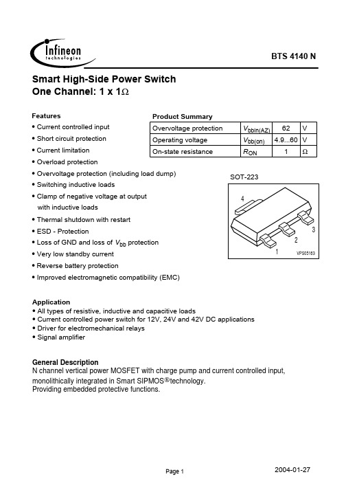
Product Summary Overvoltage protection Operating voltage On-state resistance
Vbbin(AZ) 62 V
Vbb(on) 4.9...60 V
RON
1Ω
• Overvoltage protection (including load dump) • Switching inductive loads
Page 1
2004-01-27
元器件交易网
Block Diagram
MOV-14D201K,MOV-14D431K,MOV-14D471K,MOV-14D181K,MOV-14D391K,MOV-14D511K, 规格书,Datasheet 资料
*RoHS Directive 2002/95/EC Jan. 27, 2003 including annex and RoHS Recast 2011/65/EU June 8, 2011. Specifi cations are subject to change without notice.Customers should verify actual device performance in their specifi c applications.Absolute Maximum Ratings (@ T A = 25 °C Unless Otherwise Noted)ParameterSymbol Min.Typ.Max.Unit Operating Temperature T OPR -4025+85˚C Storage Temperature T STG -4025+125˚C Rated WattageP w 0.60Watt Varistor Voltage Temperature Coeffi cient V TC 00.10.05 % / ˚C Response TimeT r 1025ns Varistor Voltage ToleranceV tol-1010%Electrical Characteristics (@ T A = 25 °C Unless Otherwise Noted)*Ro H S C O MP L I A N TBourns Part No.Max. Continuous Voltage (V)Voltage @ 1 mA DC(V)Voltage @ Class Current Max. PeakCurrent Max.Energy Max. Cap.(8/20 μs)(8/20 μs)(J)(pF)r.m.s.d.c.Min.Nom.Max.ClassCurrent(A)Max.Clamping Voltage (V)One Time 8/20 μs 1 kHz MOV-14D180K 111416182010361000 4.011100MOV-14D220K 141820222410431000 5.09100MOV-14D270K 172224273010531000 6.07400MOV-14D330K 2026303336106510007.56100MOV-14D390K 2531353943107710008.65100MOV-14D470K 30384247521093100010.04300MOV-14D560K 354550566210110100011.03600MOV-14D680K 405661687510135100014.02900MOV-14D820K 506574829050135450022.02400MOV-14D101K 60859010011050165450028.02000MOV-14D121K 7510010812013250200450032.01700MOV-14D151K 9512513515016550250450040.01300MOV-14D181K 11515016218019850300450050.01100MOV-14D201K 13017018520022550340450057.01000MOV-14D221K 14018019822024250360450060.0900MOV-14D241K 15020021624026450395450063.0830MOV-14D271K 17522524327029750455450070.0740MOV-14D301K 19025027030033050500450077.0670MOV-14D331K 21027529733036350550450085.0610MOV-14D361K 23030032436039650595450093.0560MOV-14D391K 250320351390429506504500100.0510MOV-14D431K 275350387430473507104500115.0460MOV-14D471K 300385423470517507754500125.0430MOV-14D511K 320415459510561508454500125.0390MOV-14D561K 350460504560616509254500125.0360MOV-14D621K 3855055586206825010254500125.0320MOV-14D681K 4205606126807485011204500130.0290MOV-14D751K 4606156757508255012404500143.0270MOV-14D781K 4856407027808585012904500148.0260MOV-14D821K 5106707388209025013554500157.0240MOV-14D911K 55074581991010015015004500175.0220MOV-14D102K 625825900100011005016504500190.0200MOV-14D112K 680895990110012105018154500213.0180MOV-14D152K 7509901080150013205019804500337.0150MOV-14D182K110014651620180019805029704500337.010014D 201K5Specifi cations are subject to change without notice.Customers should verify actual device performance in their specifi c applications.Product DimensionsDIMENSIONS:MM(INCHES)This is an RoHS compliant molded radial package with 100 % Sn plating on the terminations.Internal ConstructionHow to OrderMOV - 14D nn (n) K (TR)Model DesignatorMOV = Metal Oxide Varistor Disc Diameter 14D = 14 mmNominal Varistor VoltageSee Electrical Characteristics TableMultiplier of Voltage Digits 0 = No multiplier 1 = nn * 101 2 = nn * 102Varistor Voltage Tolerance K = 10 %PackagingBlank = BulkTR = Tape & Reel*Examples: MOV-14D270K = 27 V, Bulk PackMOV-14D331KTR = 330 V, T ape & Reel* Models MOV-14D911K, 102K, 112K, 152K and 182K are not available in Tape & Reel packaging.Part Number Dim. H (Max.)Dim. T (Max.)MOV-14D180K20.0(.787) 3.8(.150)MOV-14D220K 20.0(.787) 3.9(.154)MOV-14D270K 20.0(.787) 4.2(.165)MOV-14D330K 20.0(.787) 3.8(.150)MOV-14D390K20.0(.787) 4.0(.157)MOV-14D470K 20.0(.787) 4.2(.165)MOV-14D560K 20.0(.787) 4.3(.169)MOV-14D680K 20.0(.787) 4.4(.173)MOV-14D820K20.0(.787) 3.8(.150)MOV-14D101K 20.0(.787) 4.0(.157)MOV-14D121K20.0(.787) 4.2(.165)MOV-14D151K 20.0(.787) 4.4(.173)MOV-14D181K20.0(.787) 3.6(.142)MOV-14D201K 20.0(.787) 3.8(.150)MOV-14D221K 20.0(.787) 3.9(.154)MOV-14D241K 20.0(.787) 4.0(.157)MOV-14D271K 20.0(.787) 4.2(.165)MOV-14D301K20.0(.787) 4.4(.173)Part Number Dim. H (Max.)Dim. T (Max.)MOV-14D331K 20.0(.787) 4.6(.181)MOV-14D361K 20.0(.787) 4.8(.189)MOV-14D391K 20.0(.787) 5.0(.197)MOV-14D431K 20.0(.787) 5.2(.205)MOV-14D471K 20.0(.787) 5.4(.213)MOV-14D511K 20.0(.787) 5.5(.217)MOV-14D561K 22.0(.866) 6.0(.236)MOV-14D621K 22.0(.866) 6.4(.252)MOV-14D681K 22.0(.866) 6.5(.256)MOV-14D751K 22.0(.866) 6.7(.264)MOV-14D781K 22.0(.866) 6.9(.272)MOV-14D821K 22.0(.866)7.3(.287)MOV-14D911K*22.0(.866)7.7(.303)MOV-14D102K*22.0(.866)8.2(.323)MOV-14D112K*22.0(.866)8.7(.343)MOV-14D152K*22.0(.866)9.7(.382)MOV-14D182K*22.0(.866)11.7(.461)* Not available in Tape & Reel packaging.Specifi cations are subject to change without notice.Customers should verify actual device performance in their specifi c applications.1011001000101010101010Current (A)V o l t a g e (V )680560470390330270220180100100010000101010101010Current (A)V o l t a g e (V )18215211210291182178175168162156151147110010100010000101010101010Current (A)V o l t a g e (V )431391361331301271241221201181151121101820101010101010101010101010101010Performance Graphs V-I CharacteristicsMOV-14D180K to MOV-14D680KMOV-14D820K to MOV-14D431KMOV-14D471K to MOV-14D182KBournsPart Number Bourns Part Marking MOV-14D180K 14D180K MOV-14D220K 14D220K MOV-14D270K 14D270K MOV-14D330K 14D330K MOV-14D390K 14D390K MOV-14D470K 14D470K MOV-14D560K 14D560K MOV-14D680K 14D680K MOV-14D820K 14D820K MOV-14D101K 14D101K MOV-14D121K 14D121K MOV-14D151K 14D151K MOV-14D181K 14D181K MOV-14D201K 14D201K MOV-14D221K 14D221K MOV-14D241K 14D241K MOV-14D271K 14D271K MOV-14D301K 14D301K MOV-14D331K 14D331K MOV-14D361K 14D361K MOV-14D391K 14D391K MOV-14D431K 14D431K MOV-14D471K 14D471K MOV-14D511K 14D511K MOV-14D561K 14D561K MOV-14D621K 14D621K MOV-14D681K 14D681K MOV-14D751K 14D751K MOV-14D781K 14D781K MOV-14D821K 14D821K MOV-14D911K 14D821K MOV-14D102K 14D102K MOV-14D112K 14D112K MOV-14D152K 14D152K MOV-14D182K14D182KNOTE: The “5” marking on MOV products is for traceability of production assembly for quality assurance compliance.Typical Part MarkingPackaging InformationTAPE & REELItem Symbol14 mm Disc Reel Outside Diameter RD355(13.98) Reel Inner Diameter RD130(11.81) Tape Width RW55(2.165) Reel Width RW163(2.48) Pitch of Component P25.4 ± 1.0(1.00 ± 0.04) Feed Hole Pitch P012.7 ± 1.0(0.50 ± 0.04) Feed Hole Center to Pitch P18.95 ± 0.7(0.352 ± 0.3) Feed Hole Center to ComponentCenterP212.7 ± 1.0(0.50 ± 0.04)Lead to Lead Distance F7.50 ± 0.8(0.30 ± 0.03)Component AlignmentΔh4.0max.(0.157) max.Tape Width W18.0 ± 0.5(0.71 ± 0.02)Hole Down Tape Width W012.0 ± 0.8(0.47 ± 0.03)Hole Position W19.0 ± 0.5(0.35 ± 0.02)Hole Down Tape Position W23.0max.(0.12) max.Height From Center toComponent BaseH19.0 ± 1.0(0.75 ± 0.04)Seating Plane Height H016.0 ± 0.5(0.63 ± 0.02)Component Height H140.0max.(1.57) maxCrimp Length C2.60typ.(0.10) maxFeed Hole Diameter D04.0 ± 0.2(0.16 ± 0.08)Total Tape Thickness t0.6 ± 0.3(0.02 ± 0.01)Length of Clippped Height L1.0max.(0.04) maxQuantity per ReelMOV-14D180K – 14D391KMOV-14D431K - 14D182K-100050012/11Specifi cations are subject to change without notice.Customers should verify actual device performance in their specifi c applications.BULK60.0(2.36)Asia-Pacifi c:Tel: +886-2 2562-4117Fax: +886-2 2562-4116Europe:Tel: +41-41 768 5555Fax: +41-41 768 5510The Americas:Tel: +1-951 781-5500Fax: +1-951 781-5700NOTE: Models MOV-14D911K, 102K, 112K, 152K and 182K are not availablein Tape & Reel packaging.。
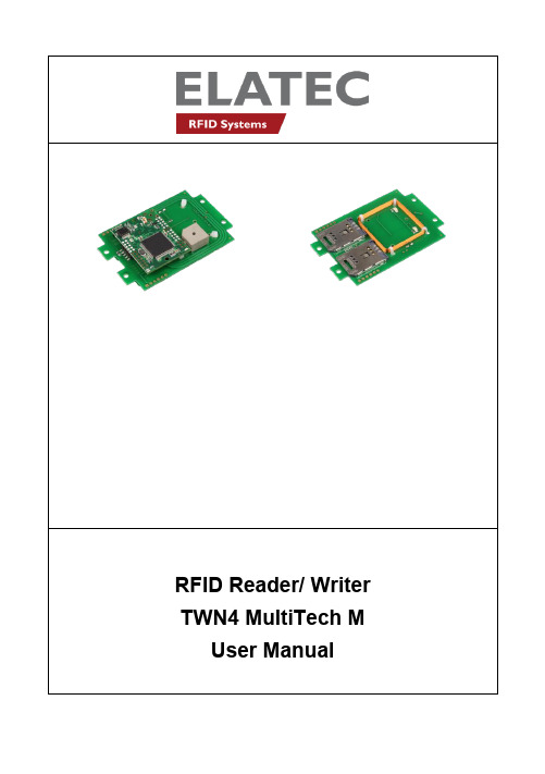
Elatec TWN4 MultiTech M User Manual
1. IntroductionThe transponder reader module TWN4 MultiTech M is a device for reading and writing RFID transponders. There are different versions of TWN4 devices available, which cover a large range of transponder types both in the frequency range of 125kHz and 13.56MHz.2. Getting Started2.1 Cable ConnectionIn order to start operating a TWN4 transponder reader, it simply has to be connected to a host.2.2 EnumerationOnce the device has been powered up, it is waiting for completion of the enumeration by the USB host. As long as the device is not enumerated, it is entering a minimum power consumption mode, where both LEDs are turned off.2.3 InitializationAfter powering up and enumeration, the device is turning on the built-in transponder reader logic. The green LED is turned on permanently. Some transponder readers need some kind of initialization, which is performed inthis step. After successful initialization, the device sounds a short sequence, which consists of a lower tone followed by a higher tone.2.4 Normal OperationAs soon as the device has completed the initialization, it is entering normal operation. During normal operation the device is searching for a transponder continuously.Detection of a TransponderIf a transponder is detected by the reader, following actions are performed ∙Send the ID to the host. By default, the USB device sends by emulating keystrokes of a keyboard.∙Sound a beep∙Turn off the green LED∙Blink the red LED for two seconds∙Turn on the green LEDWithin the two seconds timeout, where the red LED is blinking, the transponder, which just has been recognized will not be accepted again. This prevents the reader from sending identical IDs more than one time to the host.If during the two seconds timeout of the red LED a different transponder is detected, the complete sequence restarts immediately.Suspend ModeThe transponder reader supports the USB suspend mode. If the USB host is signaling suspend via the USB bus, the transponder reader is turning off most of its power consuming peripherals. During this operation mode, no detection of transponders is possible and all LEDs are turned off.Once the host is resuming to normal operation mode, this is also signaled via the USB bus. Therefore, the transponder reader will resume to normal operation, too.3. List of Antennas HF antennaLF antenna4. Compliance statementsFCC(RF module)Compliance statement:This device complies with Part 15 of the FCC Rules. Operation is subject to the following two conditions: (1) this device may not cause harmful interference, and (2) this device must accept any interference received, including interference that may cause undesired operation.Modification of equipment:The instruction manual of the host shall include the following statement: Changes or modifications made to this equipment not expressly approved by the party responsible for compliance may void the FCC authorization to operate this equipment.Information to the user:(The instruction manual of the host shall include the following statement) A compliance statement as applicable, e.g., for devices subject to part 15 of CFR 47 as specified in §15.19(a)(3), that the product complies with the rules; and the identification, by name, address and telephone number or Internet contact information, of the responsible party, as defined in §2.909. The responsible party for Supplier’s Declaration of Conformity must be located within the United States.Host devicesFCC notes for a host subject to verification or SDoC:For a host device assembled with the certified module and subject to 47 CFR Part 15 verification of class A digital devices, the following statements have to be included in the user manual and the host device has to be labelled as noted below. If the host device is subject to other authorization procedures or parts the appropriate requirements of these authorization procedures or parts apply.Important note:OEM integrator is still responsible for the FCC compliance requirements of the end product, which integrates this module. Appropriate measurements (e.g. 15B compliance) and if applicable additional equipment authorization of the host device to be addressed by the integrator/ manufacturerThe end device must be labeled with:Contains FCC ID: WP5TWN4F17Contains IC: 7948A-TWN4F17HVIN: EL20208Example for SDoC:The compliance information statement shall be included in the user's manual or as a separate sheet. In cases where the manual is provided only in a form other than paper, such as on a computer disk or over the Internet, the information required by this section may be included in the manual in that alternative form, provided the user can reasonably be expected to have the capability to access information in that form. The information may be provided electronically as permitted in §2.935.NOTE: The Commission does not have a required SDoC format. This is an example only and is provided to illustrate the type of information that may be supplied with the product at the time of marketing or importation for meeting the FCC SDoC requirement.For class B devices:FCC §15.105 (b):Note: This equipment has been tested and found to comply with the limits for a Class B digital device, pursuant to part 15 of the FCC Rules. These limits are designed to provide reasonable protection against harmful interference in a residential installation. This equipment generates, uses and can radiate radio frequency energy and, if not installed and used in accordance with the instructions, may cause harmful interference to radio communications. However, there is no guarantee that interference will not occur in a particular installation. If this equipment does cause harmful interference to radio or television reception, which can be determined by turning the equipment off and on, the user is encouraged to try to correct the interference by one or more of the following measures:- Reorient or relocate the receiving antenna.- Increase the separation between the equipment and receiver.- Connect the equipment into an outlet on a circuit different from that to which the Receiver is connected.- Consult the dealer or an experienced radio/TV technician for help.For class A devices:FCC §15.105 (b):NOTE: This equipment has been tested and found to comply with the limits for a Class A digital device, pursuant to part 15 of the FCC Rules. These limits are designed to provide reasonable protection against harmful interference when the equipment is operated in a commercial environment. This equipment generates, uses, and can radiate radio frequency energy and, if not installed and used in accordance with the instruction manual, may cause harmful interference to radio communications. Operation of this equipment in a residential area is likely to cause harmful interference in which case the user will be required to correct the interference at his own expense.CANADA:This device complies with Industry Canada’s license-exempt RSSs. Operation is subject to the following two conditions:(1) This device may not cause interference; and(2) This device must accept any interference, including interference that may cause undesired operation of the device.Le présent appareil est conforme aux CNR d’Industrie Canada applicables aux appareils radio exempts de l icence. L’exploitation est autorisée aux deux conditions suivantes:1) l’appareil ne doit pas produire de brouillage;2) l’utilisateur de l’appareil doit accepter tout brouillage radioélectrique subi, même si le brouillage est susceptible d’en compr omettre le fonctionnement. Special accessories:Where special accessories such as shielded cables and/or special connectors are required to comply with the emission limits, the instruction manual shall include appropriate instructions on the first page of the text describing the installation of the device.Simultaneous transmission:When the host product supports simultaneous-transmission operations the host manufacturer needs to check if there are additional RF exposure filing requirements due to the simultaneous transmissions. When additionalapplication filing for RF exposure compliance demonstration is not required (e. g. the RF module in combination with all simultaneously operating transmitters complies with the RFexposure simultaneous transmission SAR test exclusion requirements), the host manufacturer may do his own evaluation without any filing, using reasonable engineering judgment and testing for confirming compliance with out-of-band, restricted band, and spurious emission requirements in the simultaneous-transmission operating modes. If additional filing is required please contact the person at ELATEC GmbH responsible for certification of the RF module.5. Service AddressIn case of any technical questions, please contact: Elatec GmbHZeppelinstr. 182178 PuchheimGermanyPhone: +49 (0) 89 5529961 0Fax: +49 (0) 89 5529961 29Email: ********************6. TrademarksAll referenced brands, product names, service names and trademarks mentioned in this document are the property of their respective owners.。
XN-GW-CANOPEN 产品说明书

09/18/2015
140050 - HPL-ED2015 V15.0 EN
Terminations
Rated data
EN 61000-6-2 EN 61000-6-4 EN 61131-2
Yes, through optocoupler
°C
0 - +55
ϑ
°C
-25 - +85
5 - 95 % (indoor), Level RH-2, no condensation (for storage at 45°C)
According to IEC 60068-2-29
According to IEC 60068-2-31, free fall according to IEC 60068-2-32
IP20
EN 61100-4-2
EN 61100-4-2
EN 61100-4-4
EN 61100-4-5
EN 61100-4-6
Information about equipment supplied The delivery package for all gateways includes: 2 x end bracket XN-WEW-32/2-SW, 1 x end plate XN-ABPL
Technicaldata
10.5 Protection against electric shock
10.6 Incorporation of switching devices and components
10.7 Internal electrical circuits and connections
10.8 Connections for external conductors
WDK_Datasheet_WR401N-W14A_V1 0_201202110

nichicon FW series DATA SHEET

3300
332 10 × 20 1170 12.5 × 20 1420 12.5 × 25 1700 16 × 25 1950 16 × 35.5 2220 18 × 35.5 2360 20 × 40 2700 25 × 50 2900
4700
472 12.5 × 20 1350 12.5 × 25 1800 16 × 25 2100 16 × 31.5 2360 18 × 35.5 2490 20 × 40 2900 22 × 50 3400
Series name Type
Please refer to page 21, 22, 23 about the formed or taped product spec. Please refer to page 3 for the minimum order quantity.
Dimension table in next page.
Printed with black color letter on Gold sleeve.
D+ MAX. B P ± 0.5
Radial Lead Type
Sleeve (P.E.T.)
Bd
Pressure relief vent
(B 6.3up)
L+ MAX.
15MIN
4MIN
(mm)
BD
5
6.3
tan δ
Rated voltage (V) tan δ (MAX.)
6.3 0.28
10 0.24
16 0.20
25 0.16
35 0.14
50 0.12
For capacitance of more than 1000µF, add 0.02 for every increase of 1000µF.
STGW40N120KD;中文规格书,Datasheet资料

February 2012Doc ID 15360 Rev 51/15STGW40N120KD STGWA40N120KD40 A, 1200 V short circuit rugged IGBT with Ultrafast diodeFeatures■Low on-losses ■High current capability ■Low gate charge■Short circuit withstand time 10 µs■IGBT co-packaged with Ultrafast free-wheeling diodeApplications■Motor controlDescriptionThis high voltage and short-circuit rugged IGBT utilizes the advanced PowerMESH™ process resulting in an excellent trade-off between switching performance and low ON-state behavior.Table 1.Device summaryOrder codes Markings Package Packaging STGW40N120KD GW40N120KD TO-247Tube STGWA40N120KDGWA40N120KDTO-247 long leadsTubeContents STGW40N120KD, STGWA40N120KDContents1Electrical ratings . . . . . . . . . . . . . . . . . . . . . . . . . . . . . . . . . . . . . . . . . . . . 32Electrical characteristics . . . . . . . . . . . . . . . . . . . . . . . . . . . . . . . . . . . . . 42.1Electrical characteristics (curves) . . . . . . . . . . . . . . . . . . . . . . . . . . . . 6 3Test circuits . . . . . . . . . . . . . . . . . . . . . . . . . . . . . . . . . . . . . . . . . . . . . . . 9 4Package mechanical data . . . . . . . . . . . . . . . . . . . . . . . . . . . . . . . . . . . . 10 5Revision history . . . . . . . . . . . . . . . . . . . . . . . . . . . . . . . . . . . . . . . . . . . 142/15 Doc ID 15360 Rev 5STGW40N120KD, STGWA40N120KD Electrical ratingsDoc ID 15360 Rev 53/151 Electrical ratingsTable 2.Absolute maximum ratingsSymbol ParameterValue Unit V CES Collector-emitter voltage (V GE = 0)1200V I C (1)1. Calculated according to the iterative formula:Continuous collector current at T C = 25 °C 80A I C (1)Continuous collector current at T C = 100 °C 40A I CL (2)2.Vclamp = 80% of V CES , T j =125 °C, R G =10 Ω, V GE =15 VTurn-off latching current 85A I CP (3)3. Pulse width limited by maximum junction temperature and turn-off within RBSOAPulsed collector current 120A V GE Gate-emitter voltage±25V t SCW Short circuit withstand time, V CE = 0.5 V (BR)CEST j = 125 °C, R G = 10 Ω, V GE = 12 V 10µs P TOT Total dissipation at T C = 25 °C240W I F Diode RMS forward current at T C = 25 °C 30A I FSM Surge non repetitive forward current t p = 10 ms sinusoidal100A T jOperating junction temperature– 55 to 125°CTable 3.Thermal dataSymbol ParameterValue Unit R thj-case Thermal resistance junction-case IGBT 0.42°C/W R thj-case Thermal resistance junction-case diode 1.6°C/W R thj-ambThermal resistance junction-ambient50°C/WI C T C ()T j max ()T C–R thj c –V CE sat ()max ()T j max ()I C T C (),()×-------------------------------------------------------------------------------------------------------=Electrical characteristics STGW40N120KD, STGWA40N120KD4/15 Doc ID 15360 Rev 52 Electrical characteristicsT J = 25 °C unless otherwise specified.Table 4.StaticSymbolParameterTest conditions Min.Typ.Max.Unit V (BR)CES Collector-emitterbreakdown voltage(V GE = 0)I C = 1 mA1200V V CE(sat)Collector-emitter saturationvoltageV GE = 15 V , I C = 30 AV GE = 15 V , I C = 30 A,T J =125 °C 2.82.73.85V V V GE(th)Gate threshold voltage V CE = V GE , I C = 1mA 4.56.5V I CES Collector cut-off current (V GE = 0)V CE =1200 VV CE =1200 V , T J =125 °C 50010µA mA I GESGate-emitter leakage current (V CE = 0)V GE =± 20 V± 100nATable 5.DynamicSymbol ParameterTest conditionsMin.Typ.Max.Unit C ies C oes C res Input capacitance Output capacitance Reverse transfer capacitanceV CE = 25 V , f = 1 MHz, V GE =0-257719639.5-pF pF pF Q g Q ge Q gcTotal gate charge Gate-emitter charge Gate-collector chargeV CE = 960 V ,I C = 30 A,V GE =15 V-12622.267-nC nC nCTable 6.Switching on/off (inductive load)Symbol ParameterTest conditions Min.Typ.Max.Unit t d(on)t r (di/dt)on Turn-on delay time Current rise timeTurn-on current slope V CC = 960 V , I C = 30 A R G = 10 Ω, V GE = 15 V , (see Figure 16)-4840540-ns ns A/µs t d(on)t r (di/dt)on Turn-on delay time Current rise timeTurn-on current slope V CC = 960 V , I C = 30 A R G = 10 Ω, V GE = 15 V ,T J = 125 °C (see Figure 16)-4538665-ns ns A/µs t r (V off )t d (off )t f Off voltage rise time Turn-off delay time Current fall time V CC = 960 V , I C = 30 A R G = 10 Ω, V GE = 15 V , (see Figure 16)-84338210-ns ns ns t r (V off )t d (off )t fOff voltage rise time Turn-off delay time Current fall timeV CC = 960 V , I C = 30 A R G = 10 Ω, V GE = 15 V ,T J = 125 °C (see Figure 16)-144420360-ns ns nsSTGW40N120KD, STGWA40N120KD Electrical characteristicsDoc ID 15360 Rev 55/15Table 7.Switching energy (inductive load)Symbol ParameterTest conditions Min.Typ.Max.Unit Eon (1)E off (2)E ts 1. Eon is the turn-on losses when a typical diode is used in the test circuit in Figure 16. If the IGBT is offeredin a package with a co-pack diode, the co-pack diode is used as external diode. IGBTs and diode are at the same temperature (25°C and 125°C)2.Turn-off losses include also the tail of the collector currentT urn-on switching losses T urn-off switching losses T otal switching losses V CC = 960 V , I C = 30 A R G =10 Ω, V GE = 15 V , (see Figure 16)- 3.75.79.4-mJ mJ mJ Eon (1)E off (2)E tsT urn-on switching losses T urn-off switching losses T otal switching lossesV CC = 960 V , I C = 30 A R G =10 Ω, V GE = 15 V ,T J = 125 °C (see Figure 16)- 4.79.314-mJ mJ mJTable 8.Collector-emitter diodeSymbol ParameterTest conditions Min.Typ.Max.Unit V F Forward on-voltage I F = 20 AI F = 20 A, T J = 125 °C - 1.91.7-V V t rr Q rr I rrm Reverse recovery time Reverse recovery charge Reverse recovery current I F = 20 A, V R = 45 V ,di/dt = 100 A/µs (see Figure 19)-842355.6-ns nC A t rr Q rr I rrmReverse recovery time Reverse recovery charge Reverse recovery currentI F = 20 A, V R = 45 V ,T J = 125 °C, di/dt = 100 A/µs (see Figure 19)-1527229-ns nC AElectrical characteristics STGW40N120KD, STGWA40N120KD6/15 Doc ID 15360 Rev 52.1 Electrical characteristics (curves)Figure 4.Collector-emitter on voltage vs.Figure 5.Collector-emitter on voltage vs. Figure 6.Gate charge vs. gate-sourceFigure 7.Capacitance variationsSTGW40N120KD, STGWA40N120KD Electrical characteristicsDoc ID 15360 Rev 57/15Figure 8.Normalized gate threshold voltageFigure 9.Normalized breakdown voltage vs. Figure 10.Switching losses vs. collectorFigure 11.Switching losses vs. gateElectrical characteristics STGW40N120KD, STGWA40N120KD Figure 14.Turn-off SOA Figure 15.Forward voltage drop vs. forward8/15 Doc ID 15360 Rev 5STGW40N120KD, STGWA40N120KD Test circuitsDoc ID 15360 Rev 59/153 Test circuitsFigure 16.Test circuit for inductive loadFigure 17.Gate charge test circuitPackage mechanical data STGW40N120KD, STGWA40N120KD 4 Package mechanical dataIn order to meet environmental requirements, ST offers these devices in different grades ofECOP ACK® packages, depending on their level of environmental compliance. ECOPACK®specifications, grade definitions and product status are available at: . ECOPACKis an ST trademark.Table 9.TO-247 mechanical datamm.Dim.Min.Typ.Max.A 4.85 5.15A1 2.20 2.60b 1.0 1.40b1 2.0 2.40b2 3.0 3.40c0.400.80D19.8520.15E15.4515.75e 5.30 5.45 5.60L14.2014.80L1 3.70 4.30L218.50∅P 3.55 3.65∅R 4.50 5.50S 5.30 5.50 5.7010/15 Doc ID 15360 Rev 5分销商库存信息: STMSTGW40N120KD。
WS1N 精品系列产品使用说明书

为胜智控WS1N精品系列产品使用说明书--V1.1适用于以下型号:WS1N-20MR/MT-K-BWS1N-24MR/MT-K-BWS1N-28MR/MT-K-BWS1N-30MR/MT-K-BWS1N-32MR/MT-K-B产品目录第一章产品概述 (1)1.1产品概述 (1)1.2基本参数 (1)1.3使用环境及安装方式 (1)第二章产品展示 (2)2.1产品主要硬件说明 (2)2.2产品正面效果图................................2-3第三章电气设计参考.. (4)3.1电源及功耗 (4)3.2232通讯口说明 (4)3.3485通讯口说明 (5)3.4输入内部等效电路与接线说明 (6)3.5输出内部等效电路与接线说明.....................6-83.6模拟量输入说明 (8)3.7模拟量输出说明 (9)3.8产品接线图...................................9-10第四章编程参考 (11)4.1应用环境 (11)4.2元件号的分配和功能概要 (11)4.3特殊元件说明..................................11-124.4指令列表....................................12-144.5此版本不支持指令列表, (14)第五章常见问题及解决方案 (15)第六章保修条款 (15)第一章产品概述1.1产品概述·WS1N AC220V 系列,采用ARMCortex-M332位MISC 内核芯片,运算速度快,存储空间大。
·下载速度为9.6Kbps/19.2Kbps;直接使用三菱GX Developer 或者GX Works2编程、下载、调试、监视(不支持监控写入).·默认采用DC 24V 供电,可选择直接AC220V 交流供电(需联系客服改);输出继电器均不打开条件下,静态电流30MA;每打开一路增加13MA 电流,如1-24mr 输出继电器全打开后电流为160MA(3.84W)。
- 1、下载文档前请自行甄别文档内容的完整性,平台不提供额外的编辑、内容补充、找答案等附加服务。
- 2、"仅部分预览"的文档,不可在线预览部分如存在完整性等问题,可反馈申请退款(可完整预览的文档不适用该条件!)。
- 3、如文档侵犯您的权益,请联系客服反馈,我们会尽快为您处理(人工客服工作时间:9:00-18:30)。
Descቤተ መጻሕፍቲ ባይዱiption
Wireless Nano Router WR401N-W14A is designed for notebooks, smart phones and other portable wireless devices, it supports multiple operating modes including AP, Router, Client, Bridge and Repeater, all these features make it a unique product to create a highly efficient mobile office or entertainment network anytime anywhere. Moreover, this router is small enough to fit in your pocket, no need for any extra power adapter. With the compact and exquisite appearance, it is the best choice for your enjoyable travel and business trip.
Copyright © Shenzhen WDK Technology Co.,Ltd. All rights reserved
Wireless Nano Router
Application
Features
IEEE 802.11n, wireless speed up to 150Mbps Travel-sized design, lightweight, great for home or travel use Foldable Plug USB port can be used for charging the Smart Phone Built-in firewall featured with IP, MAC, URL filtering and ARP attack prevention to protect your PC Supports multiple operation modes in different environment Supports WEP, WPA/WPA2, WPA /WPA2- Personal encryptions(TKIP/AES) Backward compatible with 802.11b/g product
Copyright © Shenzhen WDK Technology Co.,Ltd. All rights reserved
Specifications
Wireless
Standards Data Rate Frequency Range Wireless Transmit Power Modulation Type IEEE 802.11n, IEEE 802.11g, IEEE 802.11b, CSMA/CA with ACK 11n: 150Mbps 11g: 54Mbps 11b: 11Mbps 2.4-2.4835GHz < 20dBm OFDM/CCK/16-QAM/64-QAM 150M: -68dBm@10% PER 108M: -68dBm@10% PER Receive Sensitivity 54M: -68dBm@10% PER 11M: -85dBm@8% PER 6M: -88dBm@10% PER Operation Mode Wireless Security System Requirements Router, AP, Client, Bridge, Repeater 64/128-bit WEP, WPA/WPA2, WPA /WPA2-Personal (TKIP/AES) Windows 7/Vista/XP/2000,Mac OS®, Linux or Android OS 1 x 10/100Mbps LAN/WAN Port 1 x USB 2.0 Port Reset Button 100-200V AC 50/60Hz 65mm x 92mm x 25mm 0°C~40°C (32°F~104°F) -40°C~70°C (-40°F~158°F) 10% ~ 90%, Non-condensing 5%~95%, Non-condensing CE, FCC, RoHS 1 x Wireless Nano Router 1 x Ethernet Cable
* All references to speed and range are for comparison purposes only. Product specifications, size, and shape are subject to change without notice, and actual product appearance may differ from that depicted herein.
Copyright © Shenzhen WDK Technology Co.,Ltd. All rights reserved
Hardware
Interfaces Button Power Supply Dimensions ( W x D x H )
Others
Operating Temperature Storage Temperature Relative Humidity Storage Humidity Certifications Package Contents