RHRP8120;中文规格书,Datasheet资料
PBSS5120T,215;中文规格书,Datasheet资料

Product data sheet2003 Sep 29PNP low V CEsat (BISS) transistorPBSS5120TFEATURES•Low collector-emitter saturation voltage V CEsat•High collector current capability I C and I CM•High efficiency leading to less heat generation •Reduced printed-circuit board requirements•Cost effective alternative for MOSFETs in specific applications.APPLICATIONS•Power management–DC/DC conversion–Supply line switching–Battery charger–LCD backlighting.•Peripheral drivers–Driver in low supply voltage applications (e.g. lamps and LEDs)–Inductive load drivers (e.g. relays, buzzers and motors).DESCRIPTIONPNP BISS transistor in a SOT23 plastic package providing ultra low V CEsat and R CEsat parameters.NPN complement: PBSS4120T.MARKINGNote1.* = p: made in Hong Kong.* = t: made in Malaysia.* = W: made in China.QUICK REFERENCE DATA PINNINGTYPE NUMBER MARKING CODE(1) PBSS5120T*3K SYMBOL PARAMETER MAX.UNIT V CEO collector-emitter voltage−20VI C collector current (DC)−1AI CM peak collector current−2AR CEsat equivalent on-resistance250mΩPIN DESCRIPTION1base2emitter3collectorORDERING INFORMATIONTYPE NUMBERPACKAGENAME DESCRIPTION VERSIONPBSS5120T−plastic surface mounted package; 3 leads SOT23PNP low V CEsat (BISS) transistorPBSS5120TLIMITING VALUESIn accordance with the Absolute Maximum Rating System (IEC 60134).Notes1.Device mounted on a FR4 printed-circuit board, single-sided copper, tinplated, standard footprint.2.Device mounted on a FR4 printed-circuit board, single-sided copper, tinplated, mounting pad for collector 1 cm 2.THERMAL CHARACTERISTICS Notes1.Device mounted on a FR4 printed-circuit board, single-sided copper, tinplated, standard footprint.2.Device mounted on a FR4 printed-circuit board, single-sided copper, tinplated, mounting pad for collector 1 cm 2.SYMBOL PARAMETERCONDITIONSMIN.MAX.UNITV CBO collector-base voltage open emitter −−20V V CEO collector-emitter voltage open base −−20V V EBO emitter-base voltage open collector−−5V I C collector current (DC)−−1A I CM peak collector current −−2AI BM peak base current −−200mA P tot total power dissipation T amb ≤ 25 °C; note 1−300mW T amb ≤ 25 °C; note 2−480mW T stg storage temperature −65+150°C T j junction temperature−150°C T amb operating ambient temperature−65+150°CSYMBOL PARAMETERCONDITIONS VALUE UNIT R th j-a thermal resistance from junction to ambientin free air; note 1417K/W in free air; note 2260K/WPNP low V CEsat (BISS) transistorPBSS5120TCHARACTERISTICST amb = 25 °C unless otherwise specified.Note1.Pulse test: t p ≤ 300 μs; δ ≤ 0.02.SYMBOL PARAMETERCONDITIONSMIN.TYP.MAX.UNIT I CBO collector-base cut-off current V CB = −20 V; I E = 0−−−100nA V CB = −20 V; I E = 0; T j = 150 °C −−−50μA I EBO emitter-base cut-off current V EB = −4 V; I C = 0−−−100nAh FEDC current gainV CE = −2 V; I C = −100 mA 300450−V CE = −2 V; I C = −500 mA 250350−V CE = −2 V; I C = −1 A200290−V CEsatcollector-emitter saturation voltageI C = −100 mA; I B = −1 mA −−−100mV I C = −500 mA; I B = −50 mA −−−125mV I C = −1 A; I B = −50 mA−−−250mV R CEsat equivalent on-resistance I C = −500 mA; I B = −50 mA; note 1−−250m ΩV BEon base-emitter turn-on voltage V CE = −2 V; I C = −100 mA −−−0.75V f T transition frequency I C = −100 mA; V CE = −10 V; f = 100 MHz100−−MHz C c collector capacitanceV CB = −10 V; I E = I e = 0; f = 1 MHz−−28pFPBSS5120T PNP low V CEsat (BISS) transistorPACKAGE OUTLINEPNP low V CEsat (BISS) transistorPBSS5120TDATA SHEET STATUSNotes1.Please consult the most recently issued document before initiating or completing a design.2.The product status of device(s) described in this document may have changed since this document was publishedand may differ in case of multiple devices. The latest product status information is available on the Internet at URL . DOCUMENT STATUS (1)PRODUCT STATUS (2)DEFINITIONObjective data sheet Development This document contains data from the objective specification for product development.Preliminary data sheet Qualification This document contains data from the preliminary specification. Product data sheet ProductionThis document contains the product specification.DISCLAIMERSGeneral ⎯ Information in this document is believed to be accurate and reliable. However, NXP Semiconductors does not give any representations or warranties,expressed or implied, as to the accuracy or completeness of such information and shall have no liability for the consequences of use of such information.Right to make changes ⎯ NXP Semiconductors reserves the right to make changes to informationpublished in this document, including without limitation specifications and product descriptions, at any time and without notice. This document supersedes and replaces all information supplied prior to the publication hereof.Suitability for use ⎯ NXP Semiconductors products are not designed, authorized or warranted to be suitable for use in medical, military, aircraft, space or life support equipment, nor in applications where failure or malfunction of an NXP Semiconductors product can reasonably be expected to result in personal injury, death or severe property or environmental damage. NXP Semiconductors accepts no liability for inclusion and/or use of NXP Semiconductors products in such equipment orapplications and therefore such inclusion and/or use is at the customer’s own risk.Applications ⎯ Applications that are described herein for any of these products are for illustrative purposes only. NXP Semiconductors makes no representation or warranty that such applications will be suitable for the specified use without further testing or modification.Limiting values ⎯ Stress above one or more limiting values (as defined in the Absolute Maximum Ratings System of IEC 60134) may cause permanent damage to the device. Limiting values are stress ratings only and operation of the device at these or any other conditions above those given in the Characteristics sections of this document is not implied. Exposure to limiting values for extended periods may affect device reliability.Terms and conditions of sale ⎯ NXP Semiconductors products are sold subject to the general terms and conditions of commercial sale, as published at /profile/terms, including those pertaining to warranty, intellectual property rightsinfringement and limitation of liability, unless explicitly otherwise agreed to in writing by NXP Semiconductors. In case of any inconsistency or conflict between information in this document and such terms and conditions, the latter will prevail.No offer to sell or license ⎯ Nothing in this document may be interpreted or construed as an offer to sell products that is open for acceptance or the grant, conveyance or implication of any license under any copyrights, patents or other industrial or intellectual property rights.Export control ⎯ This document as well as the item(s) described herein may be subject to export controlregulations. Export might require a prior authorization from national authorities.Quick reference data ⎯ The Quick reference data is an extract of the product data given in the Limiting values and Characteristics sections of this document, and as such is not complete, exhaustive or legally binding.NXP SemiconductorsCustomer notificationThis data sheet was changed to reflect the new company name NXP Semiconductors. No changes were made to the content, except for the legal definitions and disclaimers.Contact informationFor additional information please visit: For sales offices addresses send e-mail to: salesaddresses@© NXP B.V. 2009All rights are reserved. Reproduction in whole or in part is prohibited without the prior written consent of the copyright owner.The information presented in this document does not form part of any quotation or contract, is believed to be accurate and reliable and may be changed without notice. No liability will be accepted by the publisher for any consequence of its use. Publication thereof does not convey nor imply any license under patent- or other industrial or intellectual property rights.Printed in The Netherlands R75/01/pp7 Date of release: 2003 Sep 29 Document order number: 9397 750 11899分销商库存信息: NXPPBSS5120T,215。
AFB0812M-F00;中文规格书,Datasheet资料

Descriptions:1. Delta will not guarantee the performance of the products if the application condition fallsoutside the parameters set forth in the specification.2. A written request should be submitted to Delta prior to approval if deviation from thisspecification is required.3. Please exercise caution when handling fans. Damage may be caused when pressure is appliedto the impeller, if the fans are handled by the lead wires, or if the fans are hard-dropped to the production floor.4. Except as pertains to some special designs, there is no guarantee that the products will be freefrom any such safety problems or failures as caused by the introduction of powder, droplets of water or encroachment of insect into the hub.5. The above-mentioned conditions are representative of some unique examples and viewed as thefirst point of reference prior to all other information.6. It is very important to establish the correct polarity before connecting the fan to the powersource. Positive (+) and Negative (-). Damage may be caused to the fans if connection is with reverse polarity, as there is no foolproof method to protect against such error.7. Delta fans are not suitable where any corrosive fluids are introduced to their environment.8. Please ensure all fans are stored according to the storage temperature limits specified. Do notstore fans in a high humidity environment. We highly recommend performance testing is conducted before shipping, if the fans have been stored over 6 months.9. Not all fans are provided with the Lock Rotor Protection feature. If you impair the rotation ofthe impeller for the fans that do not have this function, the performance of those fans will lead to failure.10. Please be cautious when mounting the fan. Incorrect mounting of fans may cause excessresonance, vibration and subsequent noise.11. It is important to consider safety when testing the fans. A suitable fan guard should be fitted tothe fan to guard against any potential for personal injury.12. Except where specifically stated, all tests are carried out at relative (ambient) temperature andhumidity conditions of 25o C, 65%. The test value is only for fan performance itself.13. Be certain to connect an “over 4.7µF” capacitor to the fan externally when the application callsfor using multiple fans in parallel, to avoid any unstable power.分销商库存信息: DELTA-PRODUCT-GROUPS AFB0812M-F00。
NSi812x高可靠双通道数字隔离器数据手册说明书
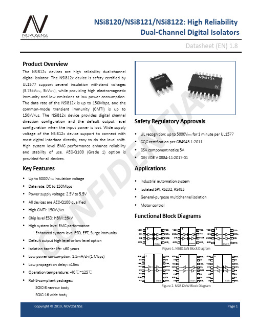
C O NF ID EN T IA LNSi8120/NSi8121/NSi8122: High ReliabilityDual-Channel Digital IsolatorsDatasheet (EN) 1.8Product OverviewThe NSi812x devices are high reliability dual-channel digital isolator. The NSi812x device is safety certified by UL1577 support several insulation withstand voltages (3.75kV rms , 5kV rms ), while providing high electromagnetic immunity and low emissions at low power consumption. The data rate of the NSi812x is up to 150Mbps, and the common-mode transient immunity (CMTI) is up to 150kV/us. The NSi812x device provides digital channel direction configuration and the default output level configuration when the input power is lost. Wide supply voltage of the NSi812x device support to connect with most digital interface directly, easy to do the level shift. High system level EMC performance enhance reliability and stability of use. AEC-Q100 (Grade 1) option is provided for all devices.Key Features• Up to 5000V rms Insulation voltage• Date rate: DC to 150Mbps• Power supply voltage: 2.5V to 5.5V • All devices are AEC-Q100 qualified • High CMTI: 150kV/us • Chip level ESD: HBM: ±6kV• High system level EMC performance:Enhanced system level ESD, EFT, Surge immunity• Default output high level or low level option • Isolation barrier life: >60 years• Low power consumption: 1.5mA/ch (1 Mbps) • Low propagation delay: <15ns • Operation temperature: -40℃~125℃ • RoHS-compliant packages:SOIC-8 narrow body SOIC-16 wide bodySafety Regulatory Approvals• UL recognition: up to 5000V rms for 1 minute per UL1577• CQC certification per GB4943.1-2011• CSA component notice 5A • DIN VDE V 0884-11:2017-01Applications• Industrial automation system • Isolated SPI, RS232, RS485• General-purpose multichannel isolation • Motor controlFunctional Block DiagramsC O NF ID EN T IA LIndex1.0 ABSOLUTE MAXIMUM RATINGS .............................................................................................................................. 3 2.0 SPECIFICATIONS ........................................................................................................................................................... 3 2.1. E LECTRICAL CHARACTERISTICS .................................................................................................................................................. 3 2.2. TYPICAL PERFORMANCE CHARACTERISTICS ........................................................................................................................... 7 2.3. P ARAMETER M EASUREMENT I NFORMATION . (8)3.0 HIGH VOLTAGE FEATURE DESCRIPTION (9)3.1. INSULATION AND SAFETY RELATED SPECIFICATIONS (9)3.2. DIN VDE V 0884-11(VDE V 0884-11):2017-01 INSULATION CHARATERISTICS ....................................................................... 9 3.3. R EGULATORY INFORMATION ................................................................................................................................................... 11 4.0 FUNCTION DESCRIPTION ..........................................................................................................................................11 5.0 APPLICATION NOTE ................................................................................................................................................... 12 5.1. PCB L AYOUT ...................................................................................................................................................................... 12 5.2. H IGH SPEED PERFORMANCE ................................................................................................................................................... 12 5.3. T YPICAL S UPPLY C URRENT E QUATIONS ..................................................................................................................................... 13 6.0 PACKAGE INFORMATION ......................................................................................................................................... 13 7.0 TAPE AND REEL INFORMATION ............................................................................................................................. 17 8.0 ORDER INFORMATION .............................................................................................................................................. 20 9.0 REVISION HISTORY . (21)C O NF ID EN T IA L1.0 ABSOLUTE MAXIMUM RATINGSPower Supply Voltage VDD1, VDD2 -0.5 6.5 V Maximum Input Voltage VINA, VINB -0.4 VDD+0.41 V Maximum Output Voltage V OUTA , V OUTB -0.4 VDD+0.41 VMaximum Input/Output Pulse VoltageVINA, VINB, V OUTA , V OUTB-0.8VDD+0.8VPulse width should be less than 100ns, and the duty cycle should be less than 10%Common-Mode Transients CMTI ±150 kV/us Output currentIo -15 15mAMaximum Surge Isolation VoltageV IOSM5.3kVOperating Temperature Topr -40125 ℃Storage Temperature Tstg -40150℃Electrostatic dischargeHBM±6000VCDM±2000V1 The maximum voltage must not exceed 6.5V.2.0 SPECIFICATIONS2.1. ELECTRICAL CHARACTERISTICS(VDD1=2.5V~5.5V, VDD2=2.5V~5.5V, Ta=-40℃ to 125℃. Unless otherwise noted, Typical values are at VDD1 = 5V, VDD2 = 5V, Ta =25℃)Power on ResetVDD POR2.2 V POR threshold as during power-upVDD HYS 0.1 V POR threshold Hysteresis Input ThresholdV IT1.6 V Input Threshold at rising edge V IT_HYS 0.4 V Input Threshold Hysteresis High Level Input Voltage V IH 2 V Low Level Input Voltage V IL 0.8 V High Level Output Voltage V OH VDD-0.3 V I OH ≤ 4mA Low Level Output VoltageV OL0.3VI OL ≤ 4mAC O NF ID EN T IA LOutput Impedance R out 50 ohm Input Pull high or low CurrentI pull 8 15 uA Start Up Time after POR trbs 40 usec Common Mode Transient ImmunityCMTI±100±150kV/us(VDD1=5V± 10%, VDD2=5V± 10%, Ta=-40℃ to 125℃. Unless otherwise noted, Typical values are at VDD1 = 5V, VDD2 = 5V, Ta = 25℃)Supply currentNSi8120 I DD1(Q0) 0.58 0.87 mAAll Input 0V for NSi8120x0 Or All Input at supply for NSi8120x1 I DD2(Q0) 1.18 1.77 mA I DD1(Q1) 2.92 4.38 mA All Input at supply for NSi8120x0 Or All Input 0V for NSi8120x1I DD2(Q1) 1.241.86mAI DD1(1M) 1.71 2.56 mA All Input with 1Mbps, C L =15pFI DD2(1M)1.382.07mAI DD1(10M) 1.78 2.67 mA All Input with 10Mbps, C L =15pF I DD2(10M)3.24.8mA I DD1(100M)2.103.15 mA All Input with 100Mbps, C L =15pFI DD2(100M)21.031.5mANSi8121/ NSi8122 I DD1(Q0) 1.031.55 mA All Input 0V for NSi812xx0 Or All Input at supply for NSi812xx1 I DD2(Q0) 1.00 1.5 mA I DD1(Q1)2.203.3 mA All Input at supply for NSi812xx0Or All Input 0V for NSi812xx1 I DD2(Q1)2.133.2 mA I DD1(1M) 1.72 2.58 mA All Input with 1Mbps, C L =15pFI DD2(1M) 1.68 2.52 mA I DD1(10M) 2.62 3.93 mA All Input with 10Mbps, C L =15pFI DD2(10M) 2.71 4.06 mA I DD1(100M) 11.01 16.5 mA All Input with 100Mbps, C L = 15pF I DD2(100M)12.8 19.2 mA Data RateDR 0 150 MbpsC O NF ID EN T IA LPropagation Delayt PLH 5 8.20 15 ns See Figure 2.7 , C L = 15pF t PHL 5 10.56 15 ns See Figure 2.7, C L = 15pF Pulse Width Distortion |t PHL – t PLH | PWD5.0nsSee Figure 2.7 , C L = 15pFRising Time t r 5.0 ns See Figure 2.7 , C L = 15pF Falling Timet f 5.0 ns See Figure 2.7 , C L = 15pFPeak Eye Diagram Jitter t JIT (PK) 350 ps Channel-to-Channel Delay Skewt SK (c2c) 2.5 nsPart-to-Part Delay Skewt SK (p2p)5.0ns(VDD1=3.3V± 10%, VDD2=3.3V± 10%, Ta=-40℃ to 125℃. Unless otherwise noted, Typical values are at VDD1 = 3.3V, VDD2 = 3.3V, Ta =25℃)Supply currentNSi8120 I DD1(Q0) 0.550.83mA All Input 0V for NSi8120x0 Or All Input at supply for NSi8120x1 I DD2(Q0) 1.12 1.68 mA I DD1(Q1) 2.87 4.3 mA All Input at supply for NSi8120x0 Or All Input 0V for NSi8120x1 I DD2(Q1)1.18 1.77mA I DD1(1M)1.72.55mA All Input with 1Mbps, C L = 15pFI DD2(1M)1.271.91 mA I DD1(10M) 1.732.6 mA All Input with 10Mbps, C L = 15pF I DD2(10M)2.413.6 mA I DD1(100M) 2.05 3.08 mA All Input with 100Mbps, C L = 15pF I DD2(100M)14.0521.08mANSi8121/ NSi8122 I DD1(Q0) 0.98 1.47 mA All Input 0V for NSi812xx0 Or All Input at supply for NSi812xx1 I DD2(Q0) 0.95 1.43 mA I DD1(Q1) 2.14 3.21 mA All Input at supply for NSi812xx0 Or All Input 0V for NSi812xx1 I DD2(Q1) 2.08 3.12 mA I DD1(1M) 1.63 2.45 mA All Input with 1Mbps, C L = 15pFI DD2(1M) 1.59 2.39 mA I (10M)2.223.33mAAll Input with 10Mbps,C O NF I D EN T IA LI DD2(10M) 2.25 3.38 mA C L = 15pFI DD1(100M) 7.57 11.36 mA All Input with 100Mbps, C L = 15pF I DD2(100M)8.5 12.75 mA Data RateDR 0 150 Mbps Minimum Pulse Width PW 5.0 nsPropagation Delayt PLH 5 9.20 15 ns See Figure 2.7 , C L = 15pF t PHL5 10.40 15 ns See Figure 2.7, C L = 15pF Pulse Width Distortion |t PHL – t PLH | PWD5.0nsSee Figure 2.7 , C L = 15pFRising Time t r 5.0 ns See Figure 2.7 , C L = 15pF Falling Timet f5.0 nsSee Figure 2.7 , C L = 15pFPeak Eye Diagram Jitter t JIT (PK) 350psChannel-to-Channel Delay Skewt SK (c2c)2.5nsPart-to-Part Delay Skew t SK (p2p)5.0ns(VDD1=2.5V± 10%, VDD2=2.5V± 10%, Ta=-40℃ to 125℃. Unless otherwise noted, Typical values are at VDD1 = 2.5V, VDD2 = 2.5V, Ta =25℃)Supply currentNSi8120I DD1(Q0) 0.53 0.8 mA All Input 0V for NSi8120x0 Or All Input at supply for NSi8120x1 I DD2(Q0) 1.11.65 mA I DD1(Q1)2.85 4.28 mA All Input at supply for NSi8120x0 Or All Input 0V for NSi8120x1 I DD2(Q1)1.15 1.73 mA I DD1(1M) 1.632.45 mA All Input with 1Mbps, C L = 15pFI DD2(1M) 1.21 1.82 mA I DD1(10M) 1.68 2.52 mA All Input with 10Mbps, C L = 15pFI DD2(10M) 2.05 3.08 mA I DD1(100M) 1.95 2.93 mA All Input with 100Mbps, C L = 15pFI DD2(100M)10.415.6mANSi8121/ NSi8122I DD1(Q0) 0.96 1.44 mA All Input 0V for NSi812xx0 Or All Input at supply for NSi812xx1I (Q0)0.931.395mAF ID EN T IA LI DD1(Q1) 2.11 3.165 mA All Input at supply for NSi812xx0Or All Input 0V for NSi812xx1 I DD2(Q1) 2.05 3.075 mA I DD1(1M) 1.58 2.37 mA All Input with 1Mbps, C L = 15pFI DD2(1M) 1.54 2.31 mA I DD1(10M) 2.02 3.03 mA All Input with 10Mbps, C L = 15pFI DD2(10M) 2.04 3.06 mA I DD1(100M) 6.03 9.045 mA All Input with 100Mbps, C L = 15pF I DD2(100M)6 9 mAData RateDR 0 150 Mbps Minimum Pulse Width PW 5.0 nsPropagation Delayt PLH 5 10 15 nsSee Figure 2.7 , C L = 15pF t PHL5 10 15nsSee Figure 2.7, C L = 15pFPulse Width Distortion |t PHL – t PLH | PWD5.0nsSee Figure 2.7 , C L = 15pFRising Time t r5.0ns See Figure 2.7 , C L = 15pF Falling Timet f5.0 ns See Figure 2.7 , C L = 15pFPeak Eye Diagram Jitter t JIT (PK)350ps Channel-to-Channel Delay Skewt SK (c2c)2.5ns Part-to-Part Delay Skew t SK (p2p)5.0ns2.2. TYPICAL PERFORMANCE CHARACTERISTICSFigure 2.1 NSi8120 VDD1 Supply Current vs Data Rate Figure 2.2 NSi8120 VDD2 Supply Current vs Data RateC OE2.3. PARAMETER MEASUREMENT INFORMATIONC LFigure 2.7 Switching Characteristics Test Circuit and WaveformFigure 2.8 Common-Mode Transient Immunity Test CircuitC O NF ID EN T IA L3.0 HIGH VOLTAGE FEATURE DESCRIPTION3.1. INSULATION AND SAFETY RELATED SPECIFICATIONSMinimum External Air Gap (Clearance)L(I01) 4.0 8.0 mm Shortest terminal-to-terminal distance through air Minimum External Tracking (Creepage)L(I02)4.08.0mmShortest terminal-to-terminal distance across the package surfaceMinimum internal gap DTI 20 um Distance through insulationTrackingResistance(Comparative Tracking Index) CTI>400VDIN EN 60112 (VDE 0303-11); IEC 60112Material GroupⅡ3.2. DIN VDE V 0884-11(VDE V 0884-11):2017-01 INSULATION CHARATERISTICSSOIC-8 SOIC-16 Installation Classification per DIN VDE 0110For Rated Mains Voltage ≤ 150V rms Ⅰto Ⅳ Ⅰto Ⅳ For Rated Mains Voltage ≤ 300V rms Ⅰto Ⅲ Ⅰto Ⅳ For Rated Mains Voltage ≤ 400V rms Ⅰto Ⅲ Ⅰto Ⅳ Climatic Classification10/105/2110/105/21 Pollution Degree per DIN VDE 0110, Table 122Maximum repetitive isolation voltageVIORM 565 849 Vpeak Input to Output Test Voltage, Method B1V IORM × 1.5 = V pd (m) , 100%production test, t ini = t m = 1 sec, partial discharge < 5 pCV pd (m)8471273VpeakInput to Output Test Voltage, Method AAfter Environmental Tests Subgroup 1V IORM × 1.2= V pd (m) , t ini = 60 sec, t m = 10 sec, partial V pd (m)6781018VpeakC O N T IA LAfter Input and /or Safety Test Subgroup 2 and Subgroup 3 V IORM × 1.2= V pd (m) , t ini = 60 sec, t m = 10 sec, partialdischarge < 5 pC V pd (m)6781018VpeakMaximum transient isolation voltage t = 60 sec VIOTM 5300 7000 Vpeak Maximum Surge Isolation VoltageTest method per IEC60065,1.2/50uswaveform, VTEST=VIOSM×1.3VIOSM53845384VpeakIsolation resistance VIO =500V RIO >109 >109 Ω Isolation capacitance f = 1MHzCIO 0.6 0.6pFInput capacitanceCI22pF Total Power Dissipation at 25℃Ps1499 mW Safety input, output, or supply currentθJA = 140 °C/W, V I = 5.5 V, T J = 150 °C, T A = 25 °C Is160mAθJA = 84 °C/W, V I = 5.5 V, T J = 150 °C, T A = 25 °C237 mA Case TemperatureTs150150℃Figure 3.2 NSi8120W/NSi8121W/NSi8122W Thermal Derating Curve, Dependence of Safety Limiting Values with Case Temperature per DIN VDE V 0884-11C O NF ID EN T IA L3.3. REGULATORY INFORMATIONThe NSi8120N/NSi8121N/NSi8122N are approved by the organizations listed in table.UL 1577 Component Recognition Program 1Approved under CSA ComponentAcceptance Notice 5ADIN VDE V 0884-11:2017-012Certified by CQC11-471543-2012 GB4943.1-2011Single Protection, 3750V rms Isolation voltageSingle Protection, 3750V rms IsolationvoltageBasic Insulation 565Vpeak, V IOSM =5384VpeakBasic insulation at 400V rms (565Vpeak)File (E500602)File (E500602)File (5024579-4880-0001)File (pending)1 In accordance with UL 1577, each NSi8120N/NSi8121N/NSi8122N is proof tested by applying an insulation test voltage ≥ 4500 Vrms for 1 sec.2 In accordance with DIN VDE V 0884-11, each NSi8120N/NSi8121N/NSi8122N is proof tested by applying an insulation test voltage ≥ 847 V peak for 1 sec(partial discharge detection limit = 5 pC). The * marking branded on the component designates DIN VDE V 0884-11 approval.The NSi8120W/NSi8121W/NSi8122W are approved by the organizations listed in table.UL 1577 Component Recognition Program 1Approved under CSAComponent Acceptance Notice5ADIN VDE V 0884-11(VDE V 0884-11):2017-012 Certified by CQC11-471543-2012 GB4943.1-2011Single Protection, 5000V rms Isolation voltageSingle Protection, 5000V rmsIsolation voltageBasic Insulation 849Vpeak, V IOSM =5384Vpeak Basic insulation at 800V rms (1131Vpeak) Reinforced insulation at 400V rms (565Vpeak)File (E500602)File (E500602)File (5024579-4880-0001)File (pending)1 In accordance with UL 1577, each NSi8120W/NSi8121W/NSi8122W is proof tested by applying an insulation test voltage ≥ 6000 V rms for 1 sec.2 In accordance with DIN VDE V 0884-11, each NSi8120W/NSi8121W/NSi8122W is proof tested by applying an insulation test voltage ≥ 1273 V peak for 1 sec(partial discharge detection limit = 5 pC). The * marking branded on the component designates DIN VDE V 0884-11 approval.4.0 FUNCTION DESCRIPTIONThe NSi812x is a Dual-channel digital isolator based on a capacitive isolation barrier technique. The digital signal is modulated with RF carrier generated by the internal oscillator at the Transmitter side. Then it is transferred through the capacitive isolation barrier and demodulated at the Receiver side.The NSi812x devices are high reliability dual-channel digital isolator with AEC-Q100 qualified. The NSi812x device is safety certified by UL1577 support several insulation withstand voltages (3.75kV rms , 5kV rms ), while providing high electromagnetic immunity and low emissions at low power consumption. The data rate of the NSi812x is up to 150Mbps, and the common-mode transient immunity (CMTI) is up to 150kV/us. The NSi812x device provides digital channel direction configuration and the default output level configuration when the input power is lost. Wide supply voltage of the NSi812x device support to connect with most digital interface directly, easy to do the level shift. High system level EMC performance enhance reliability and stability of use.The NSi812x has a default output status when VDDIN is unready and VDDOUT is ready as shown in Table 4.1, which helps for diagnosis when power is missing at the transmitter side. The output B follows the same status with the input A within 1us after powering up.C O NF ID EN T IA LCopyright © 2019, NOVOSENSEPage 12 Table 4.1 Output status vs. power statusH Ready Ready H Normal operation.L Ready Ready L XUnreadyReadyL HThe output follows the same status with the input within 60us after input side VDD1 is powered on.X Ready Unready XThe output follows the same status with the input within 60us after output side VDD2 is powered on.5.0 APPLICATION NOTE5.1. PCB LAYOUTThe NSi812x requires a 0.1 µF bypass capacitor between VDD1 and GND1, VDD2 and GND2. The capacitor should beplaced as close as possible to the package. Figure 5.1 to Figure 5.4 show the recommended PCB layout, make sure the space under the chip should keep free from planes, traces, pads and via. To enhance the robustness of a design, the user may also include resistors (50–300 Ω ) in series with the inputs and outputs if the system is excessively noisy. The series resistors also improve the system reliability such as latch-up immunity.The typical output impedance of an isolator driver channel is approximately 50 Ω, ±40%. When driving loads where transmission line effects will be a factor, output pins should be appropriately terminated with controlled impedance PCB traces.Figure5.1 Recommended PCB Layout — Top Layer Figure5.2 Recommended PCB Layout — Bottom LayerFigure5.3 Recommended PCB Layout — Top Layer Figure5.4 Recommended PCB Layout — Bottom Layer5.2. HIGH SPEED PERFORMANCEFigure 5.5 shows the eye diagram of NSi812x at 200Mbps data rate output. The result shows a typical measurement on the NSi812x with 350ps p-p jitter.C O NF ID EN T IA LFigure5.5 NSi812x Eye Diagram5.3. TYPICAL SUPPLY CURRENT EQUATIONSThe typical supply current of NSi812x can be calculated using below equations. I DD1 and I DD2 are typical supply currents measured in mA, f is data rate measured in Mbps, C L is the capacitive load measured in pFNSi8120:I DD1 = 0.19 *a1+1.45*b1+0.82*c1. I DD2 = 1.36+ VDD1*f* C L *c1*10-9When a1 is the channel number of low input at side 1, b1 is the channel number of high input at side 1, c1 is the channel number of switch signal input at side 1.NSi8121/ NSi8122:I DD1 = 0.87 +1.26*b1+0.63*c1+ VDD1*f* C L *c2*10-9I DD2 = 0.87 +1.26*b2+0.63*c2+ VDD1*f* C L *c1*10-9When b1 is the channel number of high input at side 1, c1 is the channel number of switch signal input at side 1, b2 is the channel number of high input at side 2, c2 is the channel number of switch signal input at side 2.6.0 PACKAGE INFORMATIONVDD GND 22VDD INA GND 2VDD 2Figure 6.1 NSi8120N Package Figure 6.2 NSi8121N PackageC O NF ID EN T IA LVDD INBGND 22Figure 6.3 NSi8122N PackageFigure 6.4 SOIC8 Package Shape and Dimension in millimeters (inches)Table6.1 NSi8120N/ NSi8121N/ NSi8122N Pin Configuration and DescriptionNSi8121N PIN NO.NSi8122N PIN NO.SYMBOL FUNCTION1 1 1 VDD1 Power Supply for Isolator Side 12 7 2 INA Logic Input A3 3 6 INB Logic Input B4 4 4 GND1 Ground 1, the ground reference for Isolator Side 15 5 5 GND2 Ground 2, the ground reference for Isolator Side 26 6 3 OUTB Logic Output B7 2 7 OUTA Logic Output A888VDD2Power Supply for Isolator Side 2C O NFVDD GND GND 2VDD 2GND 2GND NC NCNC VDD GND GND 2VDD 22GND NC NC NCFigure 6.5 NSi8120W Package Figure 6.6 NSi8121W PackageVDD INB GND GND 2VDD 2GND 2GND NC NC NCFigure 6.7 NSi8122W PackageFigure 6.8 WB SOIC16 Package Shape and Dimension in millimeters and (inches)C O NF ID EN T IA LTable 6.2 NSi8120W/ NSi8121W/ NSi8122W Pin Configuration and Description1 1 1 GND1 Ground 1, the ground reference for Isolator Side 12 2 2 NC No Connection.3 3 3 VDD1 Power Supply for Isolator Side 14 13 4 INA Logic Input A5 5 12 INB Logic Input B6 6 6 NC No Connection.7 7 7 GND1 Ground 1, the ground reference for Isolator Side 18 8 8 NC No Connection. 9 9 9 GND2 Ground 2, the ground reference for Isolator Side 210 10 10 NC No Connection. 11 11 11 NC No Connection. 12 12 5OUTB Logic Output A 13 4 13OUTALogic Output B 14 14 14 VDD2 Power Supply for Isolator Side 215 15 15 NC No Connection.161616GND2Ground 2, the ground reference for Isolator Side 27.0TAPE AND REEL INFORMATIONLAITNEDIFNOCC O NF ID EN T IA LFigure 7.1 Tape and Reel Information of SOIC8LAITNEDIFNOCFigure 7.2 Tape and Reel Information of WB SOIC16NF ID EN T IA L8.0 ORDER INFORMATIONNSi8120N0 3.75 2 0 150 Low -40 to 125℃ NO SOIC8 NSi8120N1 3.75 2 0 150 High -40 to 125℃ NO SOIC8 NSi8121N0 3.75 1 1 150 Low -40 to 125℃ NO SOIC8 NSi8121N1 3.75 1 1 150 High -40 to 125℃ NO SOIC8 NSi8122N0 3.75 1 1 150 Low -40 to 125℃ NO SOIC8 NSi8122N1 3.75 1 1 150 High -40 to 125℃ NO SOIC8 NSi8120W0 5 2 0 150 Low -40 to 125℃ NO WB SOIC16 NSi8120W1 5 2 0 150 High -40 to 125℃ NO WB SOIC16 NSi8121W0 5 1 1 150 Low -40 to 125℃ NO WB SOIC16 NSi8121W1 5 1 1 150 High -40 to 125℃ NO WB SOIC16 NSi8122W0 5 1 1 150 Low -40 to 125℃ NO WB SOIC16 NSi8122W1 5 1 1 150 High -40 to 125℃ NO WB SOIC16 NSi8120N0Q 3.75 2 0 150 Low -40 to 125℃ YES SOIC8 NSi8120N1Q 3.75 2 0 150 High -40 to 125℃ YES SOIC8 NSi8121N0Q 3.75 1 1 150 Low -40 to 125℃ YES SOIC8 NSi8121N1Q 3.75 1 1 150 High -40 to 125℃ YES SOIC8 NSi8122N0Q 3.75 1 1 150 Low -40 to 125℃ YES SOIC8 NSi8122N1Q 3.75 1 1 150 High -40 to 125℃ YES SOIC8 NSi8120W0Q 5 2 0 150 Low -40 to 125℃ YES WB SOIC16 NSi8120W1Q 5 2 0 150 High -40 to 125℃ YES WB SOIC16 NSi8121W0Q 5 1 1 150 Low -40 to 125℃ YES WB SOIC16 NSi8121W1Q 5 1 1 150 High -40 to 125℃ YES WB SOIC16 NSi8122W0Q 5 1 1 150 Low -40 to 125℃ YES WB SOIC16 NSi8122W1Q 5 1 1 150 High -40 to 125℃YES WB SOIC16 NOTE: All packages are RoHS-compliant with peak reflow temperatures of 260 °C according to the JEDEC industry standard classifications and peak solder temperatures. All devices are AEC-Q100 qualified.Part Number Rule:NSi(81)(2)(1)(N)(1)(Q)C O NF ID EN T IA LNSi8120/NSi8121/NSi81229.0 REVISION HISTORY1.0 Original2017/11/15 1.1 Change to Ordering information2018/3/26 1.2 Add maximum operation current specification. 2018/6/20 1.3 Change block diagram 2018/7/28 1.4 Correct Table 6.2 Pin No.2018/8/20 1.5 Add specification “Input Pull high or low Current” 2018/9/10 1.6 Add “Maximum Input/Output Pulse Voltage” 2018/10/91.7 Change to Ordering information 2018/12/20 1.8 Change Certification Information2019/06/17。
HGM8110V_8120V_8110LT_8120LT_8110CAN_8120CAN中文说明书

HGM8100N系列(HGM8110V_8120V_8110LT_8120LT_8110CAN_8120CAN)发电机组控制器用户手册目次前言 (4)1 概述 (5)2 型号对比 (5)3 性能和特点 (6)4 规格 (8)5 操作 (9)5.1 指示灯 (9)5.2 按键功能描述 (9)5.3 显示 (11)5.3.1 主显示 (11)5.3.2 参数设置菜单 (12)5.3.3 参数设置 (12)5.4 自动开机停机操作 (12)5.5 手动开机停机操作 (13)5.6 发电机组控制器开关控制过程 (15)5.6.1 HGM8120N开关控制过程 (15)5.6.1.1 手动转换过程 (15)5.6.1.2 自动转换过程 (15)5.6.2 HGM8110N开关控制过程 (15)5.6.2.1 手动控制过程 (16)5.6.2.2 自动控制过程 (16)6 保护 (17)6.1 警告报警 (17)6.2 停机报警 (18)6.3 跳闸停机报警 (19)6.4 跳闸不停机报警 (20)7 接线 (21)8 编程参数范围及定义 (22)8.1 参数设置内容及范围一览表 (23)8.2 可编程输出口可定义内容一览表 (29)8.2.1 可编程输出口可定义内容 (29)8.2.2 自定义时间段输出 (32)8.2.3 自定义组合输出 (33)8.3 可编程输入口定义内容一览表(全部为接地(B-)有效) (33)8.4 传感器选择 (36)8.5 起动成功条件选择 (37)9 参数设置 (38)10 传感器设置 (38)11 试运行 (38)12 典型应用 (40)13 安装 (42)13.1 外形尺寸 (42)13.2 电池电压输入 (42)13.3 速度传感器输入 (42)13.4 输出及扩展继电器 (42)13.5 交流电流输入 (42)13.6 耐压测试 (42)14 GSM短信报警与遥控 (43)14.1 GSM短信报警 (43)14.2 GSM短信遥控 (43)15 控制器与发动机的J1939连接 (44)15.1 CUMMINS ISB/ISBE(康明斯) (44)15.2 CUMMINS QSL9 (44)15.3 CUMMINS QSM11(进口) (44)15.4 CUMMINS QSX15-CM570 (45)15.5 CUMMINS GCS-MODBUS (45)15.6 CUMMINS QSM11(西安康明斯) (46)15.7 CUMMINS QSZ13(东风康明斯) (46)15.8 DETROIT DIESEL DDEC III / IV(底特律) (46)15.9 DEUTZ EMR2(道依茨) (47)15.10 JOHN DEERE(强鹿) (47)15.11 MTU MDEC (47)15.12 MTU ADEC(SMART模块) (47)15.13 MTU ADEC(SAM模块) (48)15.14 PERKINS(珀金斯) (48)15.15 SCANIA (48)15.16 VOLVO EDC3(沃尔沃) (49)15.17 VOLVO EDC4 (49)15.18 VOLVO-EMS2 (49)15.19 玉柴 (50)15.20 潍柴 (50)16 ETHERNET接口 (51)16.1 概述 (51)16.2 网络客户端连接方式 (51)16.3 控制器连接网线说明 (51)17 故障排除 (52)前言表1版本发展历史日期版本内容2016-07-24 1.0 开始发布。
SY8120降压电路,SY8120B1ABC规格书

应用程序信息
由于 SY8120B1 集成电路的高度集成,设计了基于该稳压芯片的应用电路相当简单。仅输入 电容器 CIN,输出电容器 COUT,输出电感 L 和反馈电阻器(R1 和 R2)需要为目标应用程 序规范。
反馈电阻分压器 R1 和 R2: 选择 r1 和 R2 以编程设定正确的输出电压。为了减少轻载下的功耗,对于这两种情况,最好 选择较大的电阻值 R1 和 R2。10kΩ 和 1MΩ 之间的值为强烈建议用于两个电阻器。如果 Vout 为 3.3V,R1=100k,然后使用以下方程式 R2 可计算为 22.1k:
1000mA 700mA 250mA
锂电池
充满电压
LED 指 静 态 封装 示灯 功耗
1节
4.2V
双灯
170uA SOP8-EP
3 节串联
12.6V
单灯
1mA SOP8-EP
1节
4.2V / 4.35V 单灯
65uA SOT23-5L
一节/二串/ 三串 单节
4.2V / 8.4V / 12.6V 4.2V
Typical Performance Characteristics
Efficiency (%)
Efficiency (%)
Efficiency (%)
Short Circuit Protection
(VIN=12V, VOUT=3.3V, Open to Short)
VOUT
2V/div
IL
Typical Applications
1
2
Figure 1. Schematic Diagram
Figure 2. Efficiency Figure
Pinout (top view)
AO4821;中文规格书,Datasheet资料
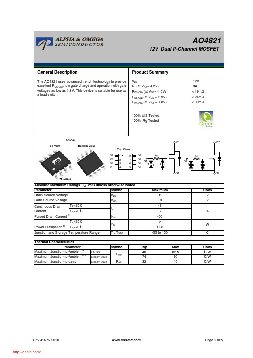
100% UIS Tested 100% Rg TestedSymbol V DS V GSI DM T J , T STGSymbolt ≤ 10s Steady-State Steady-StateR θJLW 2Maximum Junction-to-Lead°C/W°C/W Maximum Junction-to-Ambient A D 329040Maximum Junction-to-Ambient A T A =25°C T A =70°C Power DissipationBP D Pulsed Drain Current CContinuous Drain CurrentT A =25°C AI D -9-7-60V MaximumUnits Parameter Absolute Maximum Ratings T A =25°C unless otherwise noted V ±8Gate-Source Voltage Drain-Source Voltage -12°C/W R θJA 487462.5°CThermal Characteristics Units ParameterTyp Max 1.28T A =70°CJunction and Storage Temperature Range -55 to 150G1S1G2S2D1D1D2D224513867 Top ViewSOIC-8Top View Bottom ViewPin1G1D11S1RgG2D2S2RgSymbolMin Typ Max Units BV DSS -12VV DS =-12V, V GS =0V-1T J =55°C-5I GSS ±10µA V GS(th)Gate Threshold Voltage -0.35-0.53-0.85V I D(ON)-60A 1619T J =125°C22271924m Ω2330m Ωg FS 45S V SD -0.56-1V I S-3A C iss 139017402100pF C oss 230334435pF C rss 120200280pF R g0.9 1.3 1.7k ΩQ g (4.5V)151923nC Q gs 3.6 4.5 5.4nC Q gd 35.37.4nC t D(on)240ns t r 580ns t D(off)7µs t f 4.2µst rr 182226ns Q rr141720nCTHIS PRODUCT HAS BEEN DESIGNED AND QUALIFIED FOR THE CONSUMER MARKET. APPLICATIONS OR USES AS CRITICAL COMPONENTS IN LIFE SUPPORT DEVICES OR SYSTEMS ARE NOT AUTHORIZED. AOS DOES NOT ASSUME ANY LIABILITY ARISING OUT OF SUCH APPLICATIONS OR USES OF ITS PRODUCTS. AOS RESERVES THE RIGHT TO IMPROVE PRODUCT DESIGN,FUNCTIONS AND RELIABILITY WITHOUT NOTICE.Body Diode Reverse Recovery TimeDrain-Source Breakdown Voltage On state drain currentI D =-250µA, V GS =0V V GS =-4.5V, V DS =-5V V GS =-4.5V, I D =-9AReverse Transfer Capacitance I F =-9A, dI/dt=500A/µsV GS =0V, V DS =-6V, f=1MHz SWITCHING PARAMETERS Electrical Characteristics (T J =25°C unless otherwise noted)STATIC PARAMETERS ParameterConditions I DSS µA V DS =V GS I D =-250µA V DS =0V, V GS = ±8V Zero Gate Voltage Drain Current Gate-Body leakage current Forward Transconductance Diode Forward VoltageR DS(ON)Static Drain-Source On-Resistancem ΩI S =-1A,V GS =0VV DS =-5V, I D =-9A V GS =-1.8V, I D =-6AV GS =-2.5V, I D =-8A Gate resistanceV GS =0V, V DS =0V, f=1MHzTurn-Off Fall TimeTotal Gate Charge V GS =-4.5V, V DS =-6V, I D =-9AGate Source Charge Gate Drain Charge Body Diode Reverse Recovery Charge I F =-9A, dI/dt=500A/µsMaximum Body-Diode Continuous CurrentInput Capacitance Output CapacitanceTurn-On DelayTime DYNAMIC PARAMETERS Turn-On Rise Time Turn-Off DelayTime V GS =-4.5V, V DS =-6V, R L =0.67Ω,R GEN =3ΩA. The value of R θJA is measured with the device mounted on 1in 2FR-4 board with 2oz. Copper, in a still air environment with T A =25°C. The value in any given application depends on the user's specific board design.B. The power dissipation P D is based on T J(MAX)=150°C, using ≤ 10s junction-to-ambient thermal resistance.C. Repetitive rating, pulse width limited by junction temperature T J(MAX)=150°C. Ratings are based on low frequency and duty cycles to keep initialT J =25°C.D. The R θJA is the sum of the thermal impedence from junction to lead R θJL and lead to ambient.E. The static characteristics in Figures 1 to 6 are obtained using <300µs pulses, duty cycle 0.5% max.F. These curves are based on the junction-to-ambient thermal impedence which is measured with the device mounted on 1in 2 FR-4 board with 2oz. Copper, assuming a maximum junction temperature of T J(MAX)=150°C. The SOA curve provides a single pulse ratin g.TYPICAL ELECTRICAL AND THERMAL CHARACTERISTICS5101520Q g (nC)Figure 7: Gate-Charge Characteristics-V G S (V o l t s )24681012-V DS (Volts)Figure 8: Capacitance Characteristics C a p a c i t a n c e (p F )VdsCharge Gate Charge Test Circuit & WaveformD iode RVVddVddVR esistive S w itching Test C ircuit & W aveform s分销商库存信息: AOSAO4821。
HLW8110 HLW8112智能计量IC用户手册说明书
REV 1.191 / 68HLW8110/HLW8112用户手册REV 1.19REV 1.192 / 68智能计量IC1应用领域 ⏹ 智能家电设备 ⏹ 漏电检测设备 ⏹ 计量电表⏹ 计量插座 ⏹ WIFI 插座 ⏹ 充电桩 ⏹ PDU 设备 ⏹ LED 照明 ⏹ 交通路灯REV 1.193 / 682修订历史时间 修改记录版本 2018-03-16 初始版本 REV 1.00 2018-04-10 增加图表附录 REV 1.01 2018-05-25 增加协议资料 REV 1.02 2018-09-26 修改PIN 脚说明 REV 1.05 2018-09-28 重新排版 REV 1.06 2018-12-25 增加相角计算公式 REV 1.07 2019-02-13 修改字体REV 1.08 2019-02-18 更正输入通道信号输入范围值 REV 1.09 2019-02-20 增加B 通道比较器描述 REV 1.10 2019-05-21 电气特性参数修改REV 1.12 2019-10-03 增加UART 复位条件,删除uart 4800bps 设置选项 REV 1.16 2020-03-02 修改漏电检测电路 REV 1.17 2020-08-28 修订版本REV 1.18 2020-11-20 修改原理图,1K 和33NF 变更为100R 和330NF REV 1.19REV 1.194 / 68目录1 应用领域 .........................................................................................................................................2 2 修订历史 .........................................................................................................................................3 3 特性 ................................................................................................................................................. 74 概述 ................................................................................................................................................. 85 功能框图 ......................................................................................................................................... 8 6引脚配置和功能描述 (9)6.1 HLW8110芯片管脚描述 ............................................................................................................ 9 6.2 HLW8110典型应用 .................................................................................................................. 10 6.3 HLW8112芯片管脚描述 .......................................................................................................... 10 6.4HLW8112典型应用 (12)7电气特性 (12)7.1 推荐工作条件 ......................................................................................................................... 12 7.2 模拟特性 ................................................................................................................................. 13 7.3 数字特性 ................................................................................................................................. 14 7.4 极限额定值 ............................................................................................................................. 15 7.5可靠性 (15)8功能概述 (16)8.1 复位系统 ................................................................................................................................. 16 8.2 时钟系统 ................................................................................................................................. 17 8.3 模数转换 ................................................................................................................................. 17 8.4 通道切换 ................................................................................................................................. 18 8.5 有功功率 ................................................................................................................................. 18 8.6 有效值 ..................................................................................................................................... 19 8.7 视在功率和功率因素 ............................................................................................................. 20 8.8 能量计算 ................................................................................................................................. 20 8.9 过零检测、相角、电压频率测量 ......................................................................................... 21 8.10 峰值检测 ................................................................................................................................. 23 8.11 过流、过压、有功功率过载检测 ......................................................................................... 25 8.12 电压聚降检测 ......................................................................................................................... 27 8.13 均值信号 ................................................................................................................................. 29 8.14 瞬时信号和采样波形 ............................................................................................................. 30 8.15 温度传感器 ............................................................................................................................. 30 8.16比较器 (31)9寄存器说明 (32)REV 1.195 / 689.1.1 系统控制寄存器 ............................................................................................................. 34 9.1.2 计量控制寄存器 ............................................................................................................. 35 9.1.3 计量控制寄存器2 .......................................................................................................... 36 9.1.4 脉冲频率寄存器 ............................................................................................................. 37 9.1.5 无负载有功功率(潜动与启动)阈值寄存器PstartPA 、PstartPB ......................... 38 9.1.6 有功功率和视在功率增益校正寄存器 ......................................................................... 38 9.1.7 相位校正寄存器 .............................................................................. 错误!未定义书签。
SM802124UMG TR;SM802124UMG;中文规格书,Datasheet资料

Applications
• Gigabit Ethernet
Block Diagram NhomakorabeaClockWorks is a trademark of Micrel, Inc RotaryWave is a registered trademark of Multigig, Inc. Micrel Inc. • 2180 Fortune Drive • San Jose, CA 95131 • USA • tel +1 (408) 944-0800 • fax + 1 (408) 474-1000 •
- 1、下载文档前请自行甄别文档内容的完整性,平台不提供额外的编辑、内容补充、找答案等附加服务。
- 2、"仅部分预览"的文档,不可在线预览部分如存在完整性等问题,可反馈申请退款(可完整预览的文档不适用该条件!)。
- 3、如文档侵犯您的权益,请联系客服反馈,我们会尽快为您处理(人工客服工作时间:9:00-18:30)。
RHRP8120 1200 1200 1200 8
16
100
75 20 -65 to 175
UNITS V V V A
A
A
W mJ oC
©2002 Fairchild Semiconductor Corporation
/
RHRP8120 Rev. B
RHRP8120
Peak Repetitive Reverse Voltage . . . . . . . . . . . . . . . . . . . . . . . . . . . . . . . . . . . . . . . . . . . . . VRRM
Working Peak Reverse Voltage . . . . . . . . . . . . . . . . . . . . . . . . . . . . . . . . . . . . . . . . . . . . . . VRWM
Symbol
K
Features
• Hyperfast with Soft Recovery. . . . . . . . . . . . . . . . . . <55ns • Operating Temperature . . . . . . . . . . . . . . . . . . . . . . 175oC • Reverse Voltage . . . . . . . . . . . . . . . . . . . . . . . . . . . . 1200V • Avalanche Energy Rated • Planar Construction
-
-
100
µA
-
-
500
µA
trr
IF = 1A, dIF/dt = 200A/µs
-
-
55
ns
IF = 8A, dIF/dt = 200A/µs
-
-
70
ns
ta
IF = 8A, dIF/dt = 200A/µs
-
30
-
ns
tb
IF = 8A, dIF/dt = 200A/µs
-
20
-
ns
QRR
IF = 8A, dIF/dt = 200A/µs
FIGURE 1. FORWARD CURRENT vs FORWARD VOLTAGE
10
100oC
1
25oC 0.1
0.01
0.001 0
200
400
600
800
1000
VR, REVERSE VOLTAGE (V)
1200
FIGURE 2. REVERSE CURRENT vs REVERSE VOLTAGE
Formerly developmental type TA49096.
Ordering Information
PART NUMBER
PACKAGE
BRAND
RHRP8120
TO-220AC
RHRP8120
NOTE: When ordering, use the entire part number.
L
CURRENT SENSE
Q1
DUT
R
+ VDD
VDD
-
FIGURE 10. AVALANCHE ENERGY TEST CIRCUIT
dIF
IF
dt
0
trr
ta
tb
0.25 IRM IRM
FIGURE 9. trr WAVEFORMS AND DEFINITIONS
160
175
TC, CASE TEMPERATURE (oC)
FIGURE 6. CURRENT DERATING CURVE
CJ, JUNCTION CAPACITANCE (pF)
100
80
60
40
20
0
0
50
100
150
200
VR, REVERSE VOLTAGE (V)
FIGURE 7. JUNCTION CAPACITANCE vs REVERSE VOLTAGE
Electrical Specifications TC = 25oC, Unless Otherwise Specified
SYMBOL
TEST CONDITION
MIN
TYP
MAX
UNITS
VF
IF = 8A
IF = 8A, TC = 150oC
-
-
3.2
V
-
-
2.6
V
IR
VR = 1200V
VR = 1200V, TC = 150oC
Nonrepetitive Peak Surge Current . . . . . . . . . . . . . . . . . . . . . . . . . . . . . . . . . . . . . . . . . . . . . IFSM (Halfwave, 1 Phase, 60Hz)
trr
ta tb
1
4
8
IF, FORWARD CURRENT (A)
FIGURE 5. trr, ta AND tb CURVES vs FORWARD CURRENT
IF(AV), AVERAGE FORWARD CURRENT (A)
10
8 DC
6 SQ. WAVE
4
2
0
100
115
130
145
Maximum Power Dissipation . . . . . . . . . . . . . . . . . . . . . . . . . . . . . . . . . . . . . . . . . . . . . . . . . . . PD Avalanche Energy (See Figures 10 and 11) . . . . . . . . . . . . . . . . . . . . . . . . . . . . . . . . . . . . . EAVL Operating and Storage Temperature . . . . . . . . . . . . . . . . . . . . . . . . . . . . . . . . . . . . . . . . TSTG, TJ
Applications
• Switching Power Supplies • Power Switching Circuits • General Purpose
Packaging
JEDEC TO-220AC
CATHODE (FLANGE)
ANODE CATHODE
A
Absolute Maximum Ratings TC = 25oC, Unless Otherwise Specified
L
VGE
t1 t2
DUT CURRENT
RG
SENSE
+
IGBT
- VDD
FIGURE 8. trr TEST CIRCUIT
IMAX = 1A L = 40mH
R < 0.1Ω EAVL = 1/2LI2 [VR(AVL)/(VR(AVL) - VDD)]
Q1 = IGBT (BVCES > DUT VR(AVL))
80
60 trr
40 ta
20ห้องสมุดไป่ตู้
tb
0
0.5
1
4
8
IF, FORWARD CURRENT (A)
FIGURE 4. trr, ta AND tb CURVES vs FORWARD CURRENT
t, RECOVERY TIMES (ns)
120 100
80 60 40 20 0
0.5
TC = 175oC, dIF/dt = 200A/µs
DC Blocking Voltage . . . . . . . . . . . . . . . . . . . . . . . . . . . . . . . . . . . . . . . . . . . . . . . . . . . . . . . . . VR
Average Rectified (TC = 140oC)
©2002 Fairchild Semiconductor Corporation
/
RHRP8120 Rev. B
RHRP8120 Typical Performance Curves (Continued)
t, RECOVERY TIMES (ns)
60 TC = 25oC, dIF/dt = 200A/µs
-
165
-
nC
CJ RθJC
VR = 10V, IF = 0A
-
25
-
pF
-
-
2
oC/W
DEFINITIONS
VF = Instantaneous forward voltage (pw = 300µs, D = 2%). IR = Instantaneous reverse current. trr = Reverse recovery time (See Figure 9), summation of ta + tb. ta = Time to reach peak reverse current (See Figure 9). tb = Time from peak IRM to projected zero crossing of IRM based on a straight line from peak IRM through 25% of IRM (See Figure 9). QRR = Reverse Recovery Charge. CJ = Junction Capacitance. RθJC = Thermal resistance junction to case. pw = Pulse Width.