in430.h
msp430 f2132 数据手册 datasheet

MSP430F21x2 SLAS578J–NOVEMBER2007–REVISED JANUARY2012MIXED SIGNAL MICROCONTROLLERFEATURES•Low Supply Voltage Range:1.8V to3.6V•Universal Serial Communication Interface •Ultra-Low Power Consumption–Enhanced UART Supporting Auto-BaudrateDetection(LIN)–Active Mode:250µA at1MHz,2.2V–IrDA Encoder and Decoder –Standby Mode:0.7µA–Synchronous SPI–Off Mode(RAM Retention):0.1µA–I2C™•Ultra-Fast Wake-Up From Standby Mode inLess Than1µs•Brownout Detector•16-Bit RISC Architecture,62.5-ns Instruction•Serial Onboard Programming,No External Cycle Time Programming Voltage Needed,ProgrammableCode Protection by Security Fuse•Basic Clock Module Configurations•Bootstrap Loader–Internal Frequencies up to16MHz WithFour Calibrated Frequencies to±1%•On-Chip Emulation Module –Internal Very-Low-Power Low-Frequency•Family Members Include:Oscillator–MSP430F2132–32-kHz Crystal–8KB+256B Flash Memory–High-Frequency(HF)Crystal up to16MHz–512B RAM–Resonator–MSP430F2122–External Digital Clock Source–4KB+256B Flash Memory–External Resistor–512B RAM•16-Bit Timer0_A3With Three Capture/Compare–MSP430F2112Registers–2KB+256B Flash Memory•16-Bit Timer1_A2With Two Capture/Compare–256B RAMRegisters•Available in28-Pin TSSOP(PW)and32-Pin •On-Chip Comparator for Analog Signal QFN(RHB or RTV)Packages(See Table1) Compare Function or Slope Analog-to-Digital•For Complete Module Descriptions,See the (A/D)ConversionMSP430x2xx Family User's Guide,Literature •10-Bit200-ksps A/D Converter With Internal Number SLAU144Reference,Sample-and-Hold,Autoscan,andData Transfer ControllerDESCRIPTIONThe Texas Instruments MSP430™family of ultra-low-power microcontrollers consists of several devices featuring different sets of peripherals targeted for various applications.The architecture,combined with five low-power modes,is optimized to achieve extended battery life in portable measurement applications.The device features a powerful16-bit RISC CPU,16-bit registers,and constant generators that contribute to maximum code efficiency. The digitally controlled oscillator(DCO)allows wake-up from low-power modes to active mode in less than1µs. The MSP430F21x2series is an ultra-low-power microcontroller with two built-in16-bit timers,a fast10-bit A/D converter with integrated reference and a data transfer controller(DTC),a comparator,built-in communication capability using the universal serial communication interface,and up to24I/O pins.Please be aware that an important notice concerning availability,standard warranty,and use in critical applications of TexasInstruments semiconductor products and disclaimers thereto appears at the end of this data sheet.MSP430is a trademark of Texas Instruments.PRODUCTION DATA information is current as of publication date.Copyright©2007–2012,Texas Instruments Incorporated Products conform to specifications per the terms of the TexasInstruments standard warranty.Production processing does notnecessarily include testing of all parameters.MSP430F21x2SLAS578J–NOVEMBER2007–REVISED This integrated circuit can be damaged by ESD.Texas Instruments recommends that all integrated circuits be handled with appropriate precautions.Failure to observe proper handling and installation procedures can cause damage.ESD damage can range from subtle performance degradation to complete device failure.Precision integrated circuits may be more susceptible to damage because very small parametric changes could cause the device not to meet its published specifications.Table1.Available OptionsPACKAGED DEVICES(1)(2)T APLASTIC28-PIN TSSOP(PW)PLASTIC32-PIN QFN(RHB)PLASTIC32-PIN QFN(RTV)MSP430F2112IPW MSP430F2112IRHB MSP430F2112IRTV -40°C to85°C MSP430F2122IPW MSP430F2122IRHB MSP430F2122IRTVMSP430F2132IPW MSP430F2132IRHB MSP430F2132IRTVMSP430F2112TPW MSP430F2112TRHB MSP430F2112TRTV -40°C to105°C MSP430F2122TPW MSP430F2122TRHB MSP430F2122TRTVMSP430F2132TPW MSP430F2132TRHB MSP430F2132TRTV(1)For the most current package and ordering information,see the Package Option Addendum at the end of this document,or see the TIweb site at .(2)Package drawings,thermal data,and symbolization are available at /packaging.Development Tool SupportAll MSP430microcontrollers include an Embedded Emulation Module(EEM)that allows advanced debugging and programming through easy-to-use development tools.Recommended hardware options include:•Debugging and Programming Interface–MSP-FET430UIF(USB)–MSP-FET430PIF(Parallel Port)•Debugging and Programming Interface with Target Board–MSP-FET430U28(PW package)•Production Programmer–MSP-GANG4302Submit Documentation Feedback Copyright©2007–2012,Texas Instruments Incorporated12345678919202122232425262728TEST/SBWTCKDV CCP2.5/R /CA5OSC DV SSXOUT/P2.7/CA7XIN/P2.6/CA6RST/NMI/SBWTDIO P2.0/ACLK/A0/CA2P2.1/TAINCLK/SMCLK/A1/CA3P2.2/TA0.0/A2/CA4/CAOUT P1.7/TA0.2/TDO/TDI P1.6/TA0.1/TDI/TCLK P1.5/TA0.0/TMS P1.4/SMCLK/TCK P1.3/TA0.2P1.2/TA0.1P1.1/T A0.0/T A1.0P1.0/TACLK/ADC10CLK/CAOUT P2.4/TA0.2/A4/V /Ve /CA1REF+REF+P2.3/TA0.1/A3/V /Ve /CA0REF-REF-1011121314P3.0/UCB0STE/UCA0CLK/A5P3.1/UCB0SIMO/UCB0SDA P3.2/UCB0SOMI/UCB0SCL P3.3/UCB0CLK/UCA0STE15161718P3.7/TA1.1/A7P3.6/TA1.0/A6P3.5/UCA0RXD/UCA0SOMI P3.4/UCA0TXD/UCA0SIMO12345678P1.2/T A0.1P1.1/T A0.0/T A1.0P1.0/T ACLK/ADC10CLK/CAOUT NCP2.4/T A0.2/A4/V /Ve /CA1REF+REF+P2.3/T A0.1/A3/V /Ve /CA0REF-REF-NCP1.3/T A0.2XOUT/P2.7/CA7XIN/P2.6/CA6NCRST/NMI/SBWTDIO P2.0/ACLK/A0/CA2P2.1/TAINCLK/SMCLK/A1/CA3P2.2/TA0.0/A2/CA4/CAOUTDV SSN C D V C CT E S T /S B W T C K P 1.7/T A 0.2/T D O /T D I P 1.6/T A 0.1/T D I /T C L K P 1.5/T A 0.0/T M S P 1.4/S M C L K /T C KP 2.5/R /C A 5O S C P 3.1/U C B 0S I M O /U C B 0S D A P 3.2/U C B 0S O M I /U C B 0S C L P 3.3/U C B 0C L K /U C A 0S T E P 3.4/U C A 0T X D /U C A 0S I M O P 3.5/U C A 0R X D /U C A 0S O M I P 3.6/T A 1.0/A 6P 3.7/T A 1.1/A 7P 3.0/U C B 0S T E /U C A 0C L K /A 524232*********173130292827262532101112131415169MSP430F21x2SLAS578J –NOVEMBER 2007–REVISED JANUARY 2012Device Pinout,PW PackageDevice Pinout,RHB or RTV PackageCopyright ©2007–2012,Texas Instruments Incorporated Submit Documentation Feedback 3DVCCD/AVSSAVCCXINXOUTP1.xP2.xP3.xMSP430F21x2SLAS578J –NOVEMBER 2007–REVISED JANUARY 2012Functional Block Diagram4Submit Documentation Feedback Copyright ©2007–2012,Texas Instruments IncorporatedMSP430F21x2 SLAS578J–NOVEMBER2007–REVISED JANUARY2012Table2.Terminal FunctionsTERMINALNO.I/O DESCRIPTIONNAME RHB,PWRTVGeneral-purpose digital I/O pinTimer0_A3,clock signal TACLK inputP1.0/TACLK/ADC10CLK/CAOUT2121I/O Timer1_A2,clock signal TACLK inputADC10,conversion clockComparator_A+outputGeneral-purpose digital I/O pinP1.1/TA0.0/TA1.02222I/O Timer0_A3,capture:CCI0A input,compare:Out0OutputTimer1_A2,capture:CCI0A inputGeneral-purpose digital I/O pinP1.2/TA0.12323I/OTimer0_A3,capture:CCI1A input,compare:Out1OutputGeneral-purpose digital I/O pinP1.3/TA0.22424I/OTimer0_A3,capture:CCI2A input,compare:Out2OutputGeneral-purpose digital I/O pinP1.4/SMCLK/TCK2525I/O SMCLK signal outputTest Clock input for device programming and testGeneral-purpose digital I/O pinP1.5/TA0.0/TMS2626I/O Timer0_A3,compare:Out0OutputJTAG test mode select,input terminal for device programming and testGeneral-purpose digital I/O pinP1.6/TA0.1/TDI/TCLK2727I/O Timer0_A3,compare:Out1OutputJTAG test data input or test clock input in programming an testGeneral-purpose digital I/O pinP1.7/TA0.2/TDO/TDI2828I/O Timer0_A3,compare:Out2OutputJTAG test data output terminal or test data input in programming an testGeneral-purpose digital I/O pinACLK signal outputP2.0/ACLK/A0/CA286I/OADC10analog input A0Comparator_A+inputGeneral-purpose digital I/O pinSMCLK signal outputTimer0_A3,clock signal TACLK inputP2.1/TAINCLK/SMCLK/A1/CA397I/OTimer1_A2,clock signal TACLK inputADC10analog input A1Comparator_A+inputGeneral-purpose digital I/O pinTimer0_A3,capture:CCI0B input,compare:Out0OutputP2.2/TA0.0/A2/CA4/CAOUT108I/O ADC10analog input A2Comparator_A+inputComparator_A+outputGeneral-purpose digital I/O pinTimer0_A3,compare:Out1OutputP2.3/TA0.1/A3/V REF-/Ve REF-/CA01918I/OADC10analog input A3/negative referenceComparator_A+inputCopyright©2007–2012,Texas Instruments Incorporated Submit Documentation Feedback5MSP430F21x2SLAS578J–NOVEMBER2007–REVISED Table2.Terminal Functions(continued)TERMINALNO.I/O DESCRIPTIONNAME RHB,PWRTVGeneral-purpose digital I/O pinTimer0_A3,compare:Out2OutputP2.4/TA0.2/A4/V REF+/Ve REF+/CA12019I/OADC10analog input A4/positive referenceComparator_A+inputInput terminal of crystal oscillatorXIN/P2.6/CA663I/O General-purpose digital I/O pinComparator_A+inputOutput terminal of crystal oscillatorXOUT/P2.7/CA752I/O General-purpose digital I/O pinComparator_A+inputGeneral-purpose digital I/O pinP3.0/UCB0STE/UCA0CLK/A5119I/O USCI_B0slave transmit enable/USCI_A0clock input/outputADC10analog input A5General-purpose digital I/O pinP3.1/UCB0SIMO/UCB0SDA1210I/OUSCI_B0slave in/master out in SPI mode,SDA I2C data in I2C modeGeneral-purpose digital I/O pinP3.2/UCB0SOMI/UCB0SCL1311I/OUSCI_B0slave out/master in in SPI mode,SCL I2C clock in I2C modeGeneral-purpose digital I/OP3.3/UCB0CLK/UCA0STE1412I/OUSCI_B0clock input/output,USCI_A0slave transmit enableGeneral-purpose digital I/O pinP3.4/UCA0TXD/UCA0SIMO1513I/O USCI_A0transmit data output in UART mode,slave data in/master outin SPI modeGeneral-purpose digital I/O pinP3.5/UCA0RXD/UCA0SOMI1614I/O USCI_A0receive data input in UART mode,slave data out/master in inSPI modeGeneral-purpose digital I/O pinP3.6/TA1.0/A61715I/O Timer1_A2,capture:CCI0B input,compare:Out0OutputADC10analog input A6General-purpose digital I/O pinP3.7/TA1.1/A71816I/O Timer1_A2,capture:CCI1A input,compare:Out1OutputADC10analog input A7Reset or nonmaskable interrupt inputRST/NMI/SBWTDIO75ISpy-Bi-Wire test data input/output during programming and testSelects test mode for JTAG pins on Port1.The device protection fuse is TEST/SBWTCK129Iconnected to TEST.General-purpose digital I/O pinP2.5/R OSC/CA5332I/O Input for external resistor defining the DCO nominal frequencyComparator_A+inputDV CC230Digital supply voltageDV SS41Digital supply voltage4,17,20,NC NA Not connected internally.Connection to V SS is recommended.31QFN package pad(RHB,RTV packages).Connection to DV SS isQFN Pad NA Padrecommended.6Submit Documentation Feedback Copyright©2007–2012,Texas Instruments IncorporatedGeneral-Purpose Register Program Counter Stack Pointer Status Register Constant Generator General-Purpose Register General-Purpose Register General-Purpose Register PC/R0SP/R1SR/CG1/R2CG2/R3R4R5R12R13General-Purpose Register General-Purpose Register R6R7General-Purpose Register General-Purpose Register R8R9General-Purpose Register General-Purpose Register R10R11General-Purpose Register General-Purpose RegisterR14R15MSP430F21x2SLAS578J –NOVEMBER 2007–REVISED JANUARY 2012SHORT-FORM DESCRIPTIONCPUThe MSP430™CPU has a 16-bit RISC architecture that is highly transparent to the application.All operations,other than program-flow instructions,are performed as register operations in conjunction with seven addressing modes for source operand and four addressing modes for destination operand.The CPU is integrated with 16registers that provide reduced instruction execution time.The register-to-register operation execution time is one cycle of the CPU clock.Four of the registers,R0to R3,are dedicated as program counter,stack pointer,status register,and constant generator respectively.The remaining registers are general-purpose registers.Peripherals are connected to the CPU using data,address,and control buses and can be handled with all instructions.Instruction SetThe instruction set consists of 51instructions with three formats and seven address modes.Each instruction can operate on word and byte data.Table 3shows examples of the three types of instruction formats;Table 4shows the address modes.Table 3.Instruction Word FormatsINSTRUCTION FORMATEXAMPLE OPERATION Dual operands,source-destination ADD R4,R5R4+R5→R5Single operands,destination only CALL R8PC →(TOS),R8→PC Relative jump,unconditional/conditionalJNEJump-on-equal bit =0Table 4.Address Mode DescriptionsADDRESS MODE S (1)D (2)SYNTAX EXAMPLE OPERATION Register ✓✓MOV Rs,Rd MOV R10,R11R10→R11Indexed✓✓MOV X(Rn),Y(Rm)MOV 2(R5),6(R6)M(2+R5)→M(6+R6)Symbolic (PC relative)✓✓MOV EDE,TONI M(EDE)→M(TONI)Absolute ✓✓MOV &MEM,&TCDAT M(MEM)→M(TCDAT)Indirect✓MOV @Rn,Y(Rm)MOV @R10,Tab(R6)M(R10)→M(Tab+R6)M(R10)→R11Indirect autoincrement ✓MOV @Rn+,Rm MOV @R10+,R11R10+2→R10Immediate ✓MOV #X,TONIMOV #45,TONI #45→M(TONI)(1)S =source (2)D =destinationCopyright ©2007–2012,Texas Instruments Incorporated Submit Documentation Feedback 7MSP430F21x2SLAS578J–NOVEMBER2007–REVISED Operating ModesThe MSP430microcontrollers have one active mode and five software-selectable low-power modes of operation. An interrupt event can wake up the device from any of the five low-power modes,service the request,and restore back to the low-power mode on return from the interrupt program.The following six operating modes can be configured by software:•Active mode(AM)–All clocks are active.•Low-power mode0(LPM0)–CPU is disabled.–ACLK and SMCLK remain active.MCLK is disabled.•Low-power mode1(LPM1)–CPU is disabled ACLK and SMCLK remain active.MCLK is disabled.–DCO dc-generator is disabled if DCO not used in active mode.•Low-power mode2(LPM2)–CPU is disabled.–MCLK and SMCLK are disabled.–DCO dc-generator remains enabled.–ACLK remains active.•Low-power mode3(LPM3)–CPU is disabled.–MCLK and SMCLK are disabled.–DCO dc-generator is disabled.–ACLK remains active.•Low-power mode4(LPM4)–CPU is disabled.–ACLK is disabled.–MCLK and SMCLK are disabled.–DCO dc-generator is disabled.–Crystal oscillator is stopped.8Submit Documentation Feedback Copyright©2007–2012,Texas Instruments IncorporatedMSP430F21x2 SLAS578J–NOVEMBER2007–REVISED JANUARY2012Interrupt Vector AddressesThe interrupt vectors and the power-up starting address are located in the address range of0xFFFF to0xFFC0. The vector contains the16-bit address of the appropriate interrupt handler instruction sequence.If the reset vector(located at address0xFFFE)contains0xFFFF(for example,if flash is not programmed),the CPU goes into LPM4immediately after power up.Table5.Interrupt Vector AddressesINTERRUPT SOURCE INTERRUPT FLAG SYSTEM INTERRUPT WORD ADDRESS PRIORITY Power-up PORIFGExternal reset RSTIFGWatchdog WDTIFG Reset0xFFFE31,highest Flash key violation KEYV(1)PC out of range(2)NMI NMIIFG(Non)maskableOscillator fault OFIFG(Non)maskable0xFFFC30 Flash memory access violation ACCVIFG(1)(3)(Non)maskableTimer1_A2TA1CCR0CCIFG(4)Maskable0xFFFA29TA1CCR1CCIFG,Timer1_A2Maskable0xFFF828TA1CTL TAIFG(1)(4)Comparator_A+CAIFG Maskable0xFFF627Watchdog timer WDTIFG Maskable0xFFF426Timer0_A3TA0CCR0CCIFG(4)Maskable0xFFF225TA0CCR1CCIFG,Timer0_A3TA0CCR2CCIFG,Maskable0xFFF024TA0CTL TAIFG(1)(4)USCI_A0/USCI_B0receive UCA0RXIFG,Maskable0xFFEE23UCB0RXIFG(1)(5)USCI_B0I2C statusUSCI_A0/USCI_B0transmit UCA0TXIFG,Maskable0xFFEC22UCB0TXIFG(1)(6)USCI_B0I2C receive/transmitADC10ADC10IFG(4)Maskable0xFFEA210xFFE820 I/O port P2(eight flags)P2IFG.0to P2IFG.7(1)(4)Maskable0xFFE619I/O port P1(eight flags)P1IFG.0to P1IFG.7(1)(4)Maskable0xFFE4180xFFE2170xFFE016 See(7)0xFFDE15See(8)0xFFDC to0xFFC014to0,lowest(1)Multiple source flags(2)A reset is generated if the CPU tries to fetch instructions from within the module register memory address range(0x0000to0x01FF)orfrom within unused address range.(3)(non)-maskable:the individual interrupt-enable bit can disable an interrupt event,but the general interrupt enable cannot.Nonmaskable:neither the individual nor the general interrupt-enable bit will disable an interrupt event.(4)Interrupt flags are located in the module.(5)In SPI mode:UCB0RXIFG.In I2C mode:UCALIFG,UCNACKIFG,ICSTTIFG,UCSTPIFG(6)In UART/SPI mode:UCB0TXIFG.In I2C mode:UCB0RXIFG,UCB0TXIFG(7)This location is used as bootstrap loader security key(BSLSKEY).A0xAA55at this location disables the BSL completely.A zero(0x0)disables the erasure of the flash if an invalid password is supplied.(8)The interrupt vectors at addresses0xFFDC to0xFFC0are not used in this device and can be used for regular program code ifnecessary.Copyright©2007–2012,Texas Instruments Incorporated Submit Documentation Feedback9MSP430F21x2SLAS578J–NOVEMBER2007–REVISED Special Function RegistersMost interrupt and module enable bits are collected into the lowest address space.Special function register bits not allocated to a functional purpose are not physically present in the device.Simple software access is provided with this arrangement.Legendrw Bit can be read and written.rw-0,1Bit can be read and written.It is Reset or Set by PUC.rw-(0),(1)Bit can be read and written.It is Reset or Set by POR.SFR bit is not present in device.Table6.Interrupt Enable1Address76543210 00h ACCVIE NMIIE OFIE WDTIErw-0rw-0rw-0rw-0 WDTIE Watchdog timer interrupt enable.Inactive if watchdog mode is selected.Active if watchdog timer is configured in interval timer mode.OFIE Oscillator fault interrupt enableNMIIE(Non)maskable interrupt enableACCVIE Flash access violation interrupt enableTable7.Interrupt Enable2Address76543210 01h UCB0TXIE UCB0RXIE UCA0TXIE UCA0RXIErw-0rw-0rw-0rw-0UCA0RXIE USCI_A0receive-interrupt enableUCA0TXIE USCI_A0transmit-interrupt enableUCB0RXIE USCI_B0receive-interrupt enableUCB0TXIE USCI_B0transmit-interrupt enableTable8.Interrupt Flag Register1Address76543210 02h NMIIFG RSTIFG PORIFG OFIFG WDTIFGrw-0rw-(0)rw-(1)rw-1rw-(0) WDTIFG Set on watchdog timer overflow(in watchdog mode)or security key violation.Reset on V CC power-up or a reset condition at pin in reset mode.OFIFG Flag set on oscillator faultRSTIFG External reset interrupt flag.Set on a reset condition at pin in reset mode.Reset on V CC power up.PORIFG Power-on reset interrupt flag.Set on V CC power up.NMIIFG Set via pinTable9.Interrupt Flag Register2Address76543210 03h UCB0TXIFG UCB0RXIFG UCA0TXIFG UCA0RXIFGrw-1rw-0rw-1rw-0UCA0RXIFG USCI_A0receive-interrupt flagUCA0TXIFG USCI_A0transmit-interrupt flagUCB0RXIFG USCI_B0receive-interrupt flagUCB0TXIFG USCI_B0transmit-interrupt flag10Submit Documentation Feedback Copyright©2007–2012,Texas Instruments IncorporatedMemory OrganizationTable10.Memory OrganizationMSP430F2112MSP430F2122MSP430F2132Memory Size2KB4KB8KBMain:interrupt vector Flash0xFFFF to0xFFC00xFFFF to0xFFC00xFFFF to0xFFC0Main:code memory Flash0xFFFF to0xF8000xFFFF to0xF0000xFFFF to0xE000Information memory Size256Byte256Byte256ByteFlash0x10FFh to0x10000x10FFh to0x10000x10FFh to0x1000Boot memory Size1KB1KB1KBROM0x0FFF to0x0C000x0FFF to0x0C000x0FFF to0x0C00RAM Size256B512Byte512Byte0x02FF to0x02000x03FF to0x02000x03FF to0x0200Peripherals16-bit0x01FF to0x01000x01FF to0x01000x01FF to0x01008-bit0x00FF to0x00100x00FF to0x00100x00FF to0x00108-bit SFR0x000F to0x00000x000F to0x00000x000F to0x0000Bootstrap Loader(BSL)The MSP430bootstrap loader(BSL)enables users to program the flash memory or RAM using a UART serial interface.Access to the MSP430memory via the BSL is protected by user-defined password.For complete description of the features of the BSL and its implementation,see the MSP430Programming Via the Bootstrap Loader User’s Guide,literature number SLAU319.Table11.BSL Function PinsBSL FUNCTION PW PACKAGE PINS RHB,RTV PACKAGE PINSData transmit22-P1.122-P1.1Data receive10-P2.28-P2.2Flash MemoryThe flash memory can be programmed via the JTAG port,the bootstrap loader,or in-system by the CPU.The CPU can perform single-byte and single-word writes to the flash memory.Features of the flash memory include:•Flash memory has n segments of main memory and four segments of information memory(A to D)of 64bytes each.Each segment in main memory is512bytes in size.•Segments0to n may be erased in one step,or each segment may be individually erased.•Segments A to D can be erased individually,or as a group with segments0to n.Segments A to D are also called information memory.•Segment A contains calibration data.After reset,segment A is protected against programming and erasing.It can be unlocked,but care should be taken not to erase this segment if the device-specific calibration data is required.Peripherals are connected to the CPU through data,address,and control buses and can be handled using all instructions.For complete module descriptions,see the MSP430x2xx Family User's Guide(SLAU144). Oscillator and System ClockThe clock system is supported by the basic clock module that includes support for a32768-Hz watch crystal oscillator,an internal very-low-power low-frequency oscillator,an internal digitally-controlled oscillator(DCO),and a high-frequency crystal oscillator.The basic clock module is designed to meet the requirements of both low system cost and low power consumption.The internal DCO provides a fast turn-on clock source and stabilizes in less than1µs.The basic clock module provides the following clock signals:•Auxiliary clock(ACLK),sourced from a32768-Hz watch crystal,a high-frequency crystal,or the internal very-low-power LF oscillator.•Main clock(MCLK),the system clock used by the CPU.•Sub-Main clock(SMCLK),the sub-system clock used by the peripheral modules.The DCO settings to calibrate the DCO output frequency are stored in the information memory segment A. Calibration Data Stored in Information Memory Segment ACalibration data is stored for both the DCO and for ADC10organized in a tag-length-value(TLV)structure.Table12.Tags Used by the ADC Calibration TagsNAME ADDRESS VALUE DESCRIPTIONTAG_DCO_300x10F60x01DCO frequency calibration at V CC=3V and T A=30°C at calibrationTAG_ADC10_10x10DA0x08ADC10_1calibration tagTAG_EMPTY-0xFE Identifier for empty memory areasbels Used by the ADC Calibration TagsADDRESS LABEL CONDITION AT CALIBRATION/DESCRIPTION SIZEOFFSETCAL_ADC_25T85INCHx=0x1010,REF2_5=1,T A=85°C word0x0010CAL_ADC_25T30INCHx=0x1010,REF2_5=1,T A=30°C word0x000ECAL_ADC_25VREF_FACTOR REF2_5=1,T A=30°C,I VREF+=1mA word0x000CCAL_ADC_15T85INCHx=0x1010,REF2_5=0,T A=85°C word0x000ACAL_ADC_15T30INCHx=0x1010,REF2_5=0,T A=30°C word0x0008CAL_ADC_15VREF_FACTOR REF2_5=0,T A=30°C,I VREF+=0.5mA word0x0006CAL_ADC_OFFSET External V REF=1.5V,f ADC10CLK=5MHz word0x0004CAL_ADC_GAIN_FACTOR External V REF=1.5V,f ADC10CLK=5MHz word0x0002CAL_BC1_1MHz-byte0x0009CAL_DCO_1MHz-byte0x0008CAL_BC1_8MHz-byte0x0007CAL_DCO_8MHz-byte0x0006CAL_BC1_12MHz-byte0x0005CAL_DCO_12MHz-byte0x0004CAL_BC1_16MHz-byte0x0003CAL_DCO_16MHz-byte0x0002The brownout circuit is implemented to provide the proper internal reset signal to the device during power on and power off.Digital I/OThere are three8-bit I/O ports implemented—ports P1,P2,and P3:•All individual I/O bits are independently programmable.•Any combination of input,output,and interrupt condition is possible.•Edge-selectable interrupt input capability for all eight bits of port P1and P2.•Read/write access to port-control registers is supported by all instructions.•Each I/O has an individually programmable pullup/pulldown resistor.The MSP430F21x2devices provide up to24total port I/O pins available externally.See the device pinout for more information.Watchdog Timer(WDT+)The primary function of the WDT+module is to perform a controlled system restart after a software problem occurs.If the selected time interval expires,a system reset is generated.If the watchdog function is not needed in an application,the module can be disabled or configured as an interval timer and can generate interrupts at selected time intervals.ADC10The ADC10module supports fast,10-bit analog-to-digital conversions.The module implements a10-bit SAR core,sample select control,reference generator and data transfer controller,or DTC,for automatic conversion result handling allowing ADC samples to be converted and stored without any CPU intervention.Comparator_A+The primary function of the comparator_A+module is to support precision slope analog-to-digital conversions, battery-voltage supervision,and monitoring of external analog signals.Timer0_A3is a16-bit timer/counter with three capture/compare registers.Timer0_A3can support multiple capture/compares,PWM outputs,and interval timing.Timer0_A3also has extensive interrupt capabilities. Interrupts may be generated from the counter on overflow conditions and from each of the capture/compare registers.Table14.Timer0_A3Signal ConnectionsINPUT PIN NUMBER MODULE OUTPUT PIN NUMBERDEVICE INPUT MODULE MODULEOUTPUTSIGNAL INPUT NAME BLOCKPW RHB,RTV PW RHB,RTVSIGNAL21-P1.021-P1.0TACLK TACLK Timer NAACLK ACLKSMCLK SMCLK9-P2.17-P2.1TAINCLK INCLK22-P1.122-P1.1TA0CCI0A CCR0TA022-P1.122-P1.1 10-P2.28-P2.2TA0CCI0B26-P1.526-P1.5DV SS GND10-P2.28-P2.2ADC10ADC10DV CC V CC(internal)(internal) 23-P1.223-P1.2TA1CCI1A CCR1TA123-P1.223-P1.2CAOUTCCI1B27-P1.627-P1.6(internal)DV SS GND19-P2.318-P2.3ADC10ADC10DV CC V CC(internal)(internal) 24-P1.324-P1.3TA2CCI2A CCR2TA224-P1.324-P1.3ACLK(internal)CCI2B28-P1.728-P1.7DV SS GND20-P2.419-P2.4ADC10ADC10DV CC V CC(internal)(internal)Timer1_A2is a16-bit timer/counter with two capture/compare registers.Timer1_A2can support multiple capture/compares,PWM outputs,and interval timing.Timer1_A2also has extensive interrupt capabilities. Interrupts may be generated from the counter on overflow conditions and from each of the capture/compare registers.Table15.Timer1_A2Signal ConnectionsINPUT PIN NUMBER MODULE OUTPUT PIN NUMBERDEVICE INPUT MODULE MODULEOUTPUTSIGNAL INPUT NAME BLOCKPW RHB,RTV PW RHB,RTVSIGNAL21-P1.021-P1.0TACLK TACLK Timer NAACLK ACLKSMCLK SMCLK9-P2.17-P2.1TAINCLK INCLK22-P1.122-P1.1TA0CCI0A CCR0TA017-P3.615-P3.6 17-P3.615-P3.6TA0CCI0BDV SS GNDDV CC V CC18-P3.716-P3.7TA1CCI1A CCR1TA118-P3.716-P3.7CAOUTCCI1B(internal)DV SS GNDDV CC V CCUniversal Serial Communications Interface(USCI)The USCI module is used for serial data communication.The USCI module supports synchronous communication protocols like SPI(3or4pin),I2C and asynchronous communication protocols such as UART, enhanced UART with automatic baudrate detection(LIN),and IrDA.USCI_A0provides support for SPI(3or4pin),UART,enhanced UART,and IrDA.USCI_B0provides support for SPI(3or4pin)and I2C.。
SCM1241M-SCM1243MF-SCM1245MF-SCM1246MF

VCC HIN LIN COM FO
STP
UV Detect Level Shi ft
MIC
FRD Drive Circuit Drive Circuit
U,V,W
OCP
O.C. Protect
Thermal Protect
FRD
LS
Figure 1. Diagram of one of three phases in the device. SCM1240MDS-Rev. 5
Packages: Power DIP
Not to scale
Fully molded LF 2551
Heatsink pad LF2552
Functional Block Diagram
One of three phases
VB HS BootDi RB UV Detect
Input Logic
SCM1240M
SANKEN ELECTRIC CO., LTD.
http://www.sanken-ele.co.jp/en/
SCM1240M
Selection Guide
Part Number Package
ห้องสมุดไป่ตู้
High Voltage, High Current 3-Phase Motor Drivers
Output Current Continuous, IO(max) (A) 10 15 20 30 Pulsed, IOP (max) (A) 20 30 30 45
SCM1240MDS-Rev. 5
SANKEN ELECTRIC CO., LTD.
2
SCM1240M
High Voltage, High Current 3-Phase Motor Drivers
ls和hc区别

74LS属于TTL类型的集成电路,而74HC属于CMOS集成电路。
LS、HC 二者高电平低电平定义不同,HC高电平规定为0.7倍电源电压,低电平规定为0.3倍电源电压。
LS规定高电平为2.0V,低电平为0.8V。
带负载特性不同。
HC上拉下拉能力相同,LS上拉弱而下拉强。
输入特性不同。
HC输入电阻很高,输入开路时电平不定。
LS输入内部有上拉,输入开路时为高电平。
(1)74LS系列是“低功耗肖特基TTL”,统称74LS系列。
其改进型为“先进低功耗肖特基TTL”,既74ALS系列,它的性能比74LS更好。
(2)74HC系列,它具有CMOS的低功耗和相当于74LS高速度的性能,属于一种高速低功耗产品。
(3)上述两者的工作频率都在30mHz以下,74ALS略高,可达50mHz。
(4)但它们的工作电压却大不相同:74LS系列为5V,74HC系列为2~6V。
(5)扇出能力:74LS系列为20,而74HC系列在直流时则高达1000以上,但在交流时很低,由工作频率决定从网上下的,集合了一下系列电平典型传输延迟ns 最大驱动电流(-Ioh/Lol)mAAHC CMOS 8.5 -8/8AHCT COMS/TTL 8.5 -8/8HC COMS 25 -8/8HCT COMS/TTL 25 -8/8ACT COMS/TTL 10 -24/24F TTL 6.5 -15/64ALS TTL 10 -15/64LS TTL 18 -15/24注:同型号的74系列、74HC系列、74LS系列芯片,逻辑功能上是一样的。
74LSxx的使用说明如果找不到的话,可参阅74xx或74HCxx的使用说明。
有些资料里包含了几种芯片,如74HC161资料里包含了74HC160、74HC161、74HC162、74HC163四种芯片的资料。
找不到某种芯片的资料时,可试着查看一下临近型号的芯片资料。
7400 QUAD 2-INPUT NAND GATES 与非门7401 QUAD 2-INPUT NAND GATES OC 与非门7402 QUAD 2-INPUT NOR GATES 或非门7403 QUAD 2-INPUT NAND GATES 与非门7404 HEX INVERTING GATES 反向器7406 HEX INVERTING GATES HV 高输出反向器7408 QUAD 2-INPUT AND GATE 与门7409 QUAD 2-INPUT AND GATES OC 与门7410 TRIPLE 3-INPUT NAND GATES 与非门7411 TRIPLE 3-INPUT AND GATES 与门74121 ONE-SHOT WITH CLEAR 单稳态74132 SCHMITT TRIGGER NAND GATES 触发器与非门7414 SCHMITT TRIGGER INVERTERS 触发器反向器74153 4-LINE TO 1 LINE SELECTOR 四选一74155 2-LINE TO 4-LINE DECODER 译码器74180 PARITY GENERATOR/CHECKER 奇偶发生检验74191 4-BIT BINARY COUNTER UP/DOWN 计数器7420 DUAL 4-INPUT NAND GATES 双四输入与非门7426 QUAD 2-INPUT NAND GATES 与非门7427 TRIPLE 3-INPUT NOR GATES 三输入或非门7430 8-INPUT NAND GATES 八输入端与非门7432 QUAD 2-INPUT OR GATES 二输入或门7438 2-INPUT NAND GATE BUFFER 与非门缓冲器7445 BCD-DECIMAL DECODER/DRIVER BCD译码驱动器7474 D-TYPE FLIP-FLOP D型触发器7475 QUAD LATCHES 双锁存器7476 J-K FLIP-FLOP J-K触发器7485 4-BIT MAGNITUDE COMPARATOR 四位比较器7486 2-INPUT EXCLUSIVE OR GATES 双端异或门74HC00 QUAD 2-INPUT NAND GATES 双输入与非门74HC02 QUAD 2-INPUT NOR GATES 双输入或非门74HC03 2-INPUT OPEN-DRAIN NAND GATES 与非门74HC04 HEX INVERTERS 六路反向器74HC05 HEX INVERTERS OPEN DRAIN 六路反向器74HC08 2-INPUT AND GATES 双输入与门74HC107 J-K FLIP-FLOP WITH CLEAR J-K触发器74HC109A J-K FLIP-FLOP W/PRESET J-K触发器74HC11 TRIPLE 3-INPUT AND GATES 三输入与门74HC112 DUAL J-K FLIP-FLOP 双J-K触发器74HC113 DUAL J-K FLIP-FLOP PRESET 双JK触发器74HC123A RETRIGGERABLE MONOSTAB 可重触发单稳74HC125 TRI-STATE QUAD BUFFERS 四个三态门74HC126 TRI-STATE QUAD BUFFERS 六三态门74HC132 2-INPUT TRIGGER NAND 施密特触发与非门74HC133 13-INPUT NAND GATES 十三输入与非门74HC137 3-TO-8 DECODERS W/LATCHES 3-8线译码器74HC138 3-8 LINE DECODER 3线至8线译码器74HC139 2-4 LINE DECODER 2线至4线译码器74HC14 TRIGGERED HEX INVERTER 六触发反向器74HC147 10-4 LINE PRIORITY ENCODER 10-4编码器74HC148 8-3 LINE PRIORITY ENCODER 8-3编码器74HC149 8-8 LINE PRIORITY ENCODER 8-8编码器74HC151 8-CHANNEL DIGITAL MUX 8通道多路器74HC153 DUAL 4-INPUT MUX 双四输入多路器74HC154 4-16 LINE DECODER 4线至16线译码器74HC155 2-4 LINE DECODER 2线至4线译码器74HC157 QUAD 2-INPUT MUX 四个双端多路器74HC161 BINARY COUNTER 二进制计数器74HC163 DECADE COUNTERS 十进制计数器74HC164 SERIAL-PARALLEL SHIFT REG 串入并出74HC165 PARALLEL-SERIAL SHIFT REG 并入串出74HC166 SERIAL-PARALLEL SHIFT REG 串入并出74HC173 TRI-STATE D FLIP-FLOP 三态D触发器74HC174 HEX D FLIP-FLOP W/CLEAR 六D触发器74HC175 HEX D FLIP-FLOP W/CLEAR 六D触发器74HC181 ARITHMETIC LOGIC UNIT 算术逻辑单元74HC182 LOOK AHEAD CARRYGENERATR 进位发生器74HC190 BINARY UP/DN COUNTER 二进制加减计数器74HC191 DECADE UP/DN COUNTER 十进制加减计数器74HC192 DECADE UP/DN COUNTER 十进制加减计数器74HC193 BINARY UP/DN COUNTER 二进制加减计数器74HC194 4BIT BI-DIR SHIFT 4位双向移位寄存器74HC195 4BIT PARALLEL SHIFT 4位并行移位寄存器74HC20 QUAD 4-INPUT NAND GATE 四个四入与非门74HC221A NON-RETRIG MONOSTAB 不可重触发单稳74HC237 3-8 LINE DECODER 地址锁3线至8线译码器74HC242/243 TRI-STAT TRANSCEIVER 三态收发器74HC244 OCTAL 3-STATE BUFFER 八个三态缓冲门74HC245 OCTAL 3-STATE TRANSCEIVER 三态收发器74HC251 8-CH 3-STATE MUX 8路3态多路器74HC253 DUAL 4-CH 3-STATE MUX 4路3态多路器74HC257 QUAD 2-CH 3-STATE MUX 4路3态多路器74HC258 2-CH 3-STATE MUX 2路3态多路器74HC259 3-8 LINE DECODER 8位地址锁存译码器74HC266A 2-INPUT EXCLUSIVE NOR GATE 异或非74HC27 TRIPLE 3-INPUT NOR GATE三个3输入或非门74HC273 OCTAL D FLIP-FLOP CLEAR 8路D触发器74HC280 9BIT ODD/EVEN GENERATOR 奇偶发生器74HC283 4BIT BINARY ADDER CARRY 四位加法器74HC299 3-STATE UNIVERSAL SHIFT 三态移位寄存74HC30 8-INPUT NAND GATE 8输入端与非门74HC32 QUAD 2-INPUT OR GATE 四个双端或门74HC34 NON-INVERTER 非反向器74HC354 8-CH 3-STATE MUX 8路3态多路器74HC356 8-CH 3-STATE MUX 8路3态多路器74HC365 HEX 3-STATE BUFFER 六个三态缓冲门74HC366 3-STATE BUFFER INVERTER 缓冲反向器74HC367 3-STATE BUFFER INVERTER 缓冲反向器74HC368 3-STATE BUFFER INVERTER 缓冲反向器74HC373 3-STATE OCTAL D LATCHES 三态D型锁存器74HC374 3-STATE OCTAL D FLIPFLOP 三态D触发器74HC393 4-BIT BINARY COUNTER 4位二进制计数器74HC4016 QUAD ANALOG SWITCH 四路模拟量开关74HC4020 14-Stage Binary Counter 14输出计数器74HC4017 Decade Counter/Divider with 10 Decoded Outputs 十进制计数器带10个译码输出端74HC4040 12 Stage Binary Counter 12出计数器74HC4046 PHASE LOCK LOOP 相位监测输出器74HC4049 LEVEL DOWN CONVERTER 电平变低器74HC4050 LEVEL DOWN CONVERTER 电平变低器74HC4051 8-CH ANALOG MUX 8通道多路器74HC4052 4-CH ANALOG MUX 4通道多路器74HC4053 2-CH ANALOG MUX 2通道多路器74HC4060 14-STAGE BINARY COUNTER 14阶BIN计数74HC4066 QUAD ANALOG MUX 四通道多路器74HC4075 TRIPLE 3-INPUT OR GATE 3输入或门74HC42 BCD TO DECIMAL BCD转十进制译码器74HC423A RETRIGGERABLE MONOSTAB 可重触发单稳74HC4511 BCD-7 SEG DRIVER/DECODER 7段译码器74HC4514 4-16 LINE DECODER 4至16线译码器74HC4538A RETRIGGERAB MONOSTAB 可重触发单稳74HC4543 LCD BCD-7 SEG LCD用的BCD-7段译码驱动74HC51 AND OR GATE INVERTER 与或非门74HC521 8BIT MAGNITUDE COMPARATOR 判决定路74HC533 3-STATE D LATCH 三态D锁存器74HC534 3-STATE D FLIP-FLOP 三态D型触发器74HC540 3-STATE BUFFER 三态缓冲器74HC541 3-STATE BUFFER INVERTER三态缓冲反向器74HC58 DUAL AND OR GATE 与或门74HC589 3STATE 8BIT SHIFT 8位移位寄存三态输出74HC594 8BIT SHIFT REG 8位移位寄存器74HC595 8BIT SHIFT REG 8位移位寄存器出锁存74HC597 8BIT SHIFT REG 8位移位寄存器入锁存74HC620 3-STATE TRANSCEIVER 反向3态收发器74HC623 3-STATE TRANSCEIVER 八路三态收发器74HC640 3-STATE TRANSCEIVER 反向3态收发器74HC643 3-STATE TRANSCEIVER 八路三态收发器74HC646 NON-INVERT BUS TRANSCEIVER 总线收发器74HC648 INVERT BUS TRANCIVER 反向总线收发器74HC688 8BIT MAGNITUDE COMPARATOR 8位判决电路74HC7266 2-INPUT EXCLUSIVE NOR GATE 异或非门74HC73 DUAL J-K FLIP-FLOP W/CLEAR 双JK触发器74HC74A PRESET/CLEAR D FLIP-FLOP 双D触发器74HC75 4BIT BISTABLE LATCH 4位双稳锁存器74HC76 PRESET/CLEAR JK FLIP-FLOP 双JK触发器74HC85 4BIT MAGNITUDE COMPARATOR 4位判决电路74HC86 2INPUT EXCLUSIVE OR GATE 2输入异或门74HC942 BAUD MODEM 300BPS低速调制解调器74HC943 300 BAUD MODEM 300BPS低速调制解调器74LS00 QUAD 2-INPUT NAND GATES 与非门74LS02 QUAD 2-INPUT NOR GATES 或非门74LS03 QUAD 2-INPUT NAND GATES 与非门74LS04 HEX INVERTING GATES 反向器74LS05 HEX INVERTERS OPEN DRAIN 六路反向器74LS08 QUAD 2-INPUT AND GATE 与门74LS09 QUAD 2-INPUT AND GATES OC 与门74LS10 TRIPLE 3-INPUT NAND GATES 与非门74LS109 QUAD 2-INPUT AND GATES OC 与门74LS11 TRIPLE 3-INPUT AND GATES 与门74LS112 DUAL J-K FLIP-FLOP 双J-K触发器74LS113 DUAL J-K FLIP-FLOP PRESET 双JK触发器74LS114 NEGATIVE J-K FLIP-FLOP 负沿J-K触发器74LS122 Retriggerable Monostab 可重触发单稳74LS123 Retriggerable Monostable 可重触发单稳74LS125 TRI-STATE QUAD BUFFERS 四个三态门74LS13 QUAL 4-in NAND TRIGGER 4输入与非触发器74LS160 BCD DECADE 4BIT BIN COUNTERS 计数器74LS136 QUADRUPLE 2-INPUT XOR GATE 异或门74LS138 3-8 LINE DECODER 3线至8线译码器74LS139 2-4 LINE DECODER 2线至4线译码器74LS14 TRIGGERED HEX INVERTER 六触发反向器74HC147 10-4 LINE PRIORITY ENCODER 10-4编码器74HC148 8-3 LINE PRIORITY ENCODER 8-3编码器74HC149 8-8 LINE PRIORITY ENCODER 8-8编码器74LS151 8-CHANNEL DIGITAL MUX 8通道多路器74LS153 DUAL 4-INPUT MUX 双四输入多路器74LS155 2-4 LINE DECODER 2线至4线译码器74LS156 2-4 LINE DECODER/DEMUX 2-4译码器74LS157 QUAD 2-INPUT MUX 四个双端多路器74LS158 2-1 LINE MUX 2-1线多路器74LS160A BINARY COUNTER 二进制计数器74LS161A BINARY COUNTER 二进制计数器74LS162A BINARY COUNTER 二进制计数器74LS163A DECADE COUNTERS 十进制计数器74LS164 SERIAL-PARALLEL SHIFT REG 串入并出74LS168 BI-DIRECT BCD TO DECADE 双向计数器74LS169 4BIT UP/DN BIN COUNTER 四位加减计数器74LS173 TRI-STATE D FLIP-FLOP 三态D触发器74LS174 HEX D FLIP-FLOP W/CLEAR 六D触发器74LS175 HEX D FLIP-FLOP W/CLEAR 六D触发器74LS190 BINARY UP/DN COUNTER 二进制加减计数器74LS191 DECADE UP/DN COUNTER 十进制加减计数器74LS192 DECADE UP/DN COUNTER 十进制加减计数器74LS193 BINARY UP/DN COUNTER 二进制加减计数器74LS194A 4BIT BI-DIR SHIFT 4位双向移位寄存器74LS195A 4BIT PARALLEL SHIFT4位并行移位寄存器74LS20 QUAD 4-INPUT NAND GATE 四个四入与非门74LS21 4-INPUT AND GATE 四输入端与门74LS240 OCTAL 3-STATE BUFFER 八个三态缓冲门74LS244 OCTAL 3-STATE BUFFER 八个三态缓冲门74LS245 OCTAL 3-STATE TRANSCEIVER 三态收发器74LS253 DUAL 4-CH 3-STATE MUX 4路3态多路器74LS256 4BIT ADDRESS LATCH 四位可锁存锁存器74LS257 QUAD 2-CH 3-STATE MUX 4路3态多路器74LS258 2-CH 3-STATE MUX 2路3态多路器74LS27 TRIPLE 3-INPUT NOR GATES 三输入或非门74LS279 QUAD R-S LATCHES 四个RS非锁存器74LS28 QUAD 2-INPUT NOR BUFFER 四双端或非缓冲74LS283 4BIT BINARY ADDER CARRY 四位加法器74LS30 8-INPUT NAND GATES 八输入端与非门74LS32 QUAD 2-INPUT OR GATES 二输入或门74LS352 4-1 LINE SELECTOR/MUX 4-1线选择多路器74LS365 HEX 3-STATE BUFFER 六个三态缓冲门74LS367 3-STATE BUFFER INVERTER 缓冲反向器74LS368A 3-STATE BUFFER INVERTER 缓冲反向器74LS373 OCT LATCH W/3-STATE OUT三态输出锁存器74LS76 Dual JK Flip-Flop w/set 2个JK触发器74LS379 QUAD PARALLEL REG 四个并行寄存器74LS38 2-INPUT NAND GATE BUFFER 与非门缓冲器74LS390 DUAL DECADE COUNTER 2个10进制计数器74LS393 DUAL BINARY COUNTER 2个2进制计数器74LS42 BCD TO DECIMAL BCD转十进制译码器74LS48 BCD-7 SEG BCD-7段译码器74LS49 BCD-7 SEG BCD-7段译码器74LS51 AND OR GATE INVERTER 与或非门74LS540 OCT Buffer/Line Driver 8路缓冲驱动器74LS541 OCT Buffer/LineDriver 8路缓冲驱动器74LS74 D-TYPE FLIP-FLOP D型触发器74LS682 8BIT MAGNITUDE COMPARATOR 8路比较器74LS684 8BIT MAGNITUDE COMPARATOR 8路比较器74LS75 QUAD LATCHES 双锁存器74LS83A 4BIT BINARY ADDER CARRY 四位加法器74LS85 4BIT MAGNITUDE COMPARAT 4位判决电路74LS86 2INPUT EXCLUSIVE OR GATE 2输入异或门74LS90 DECADE/BINARY COUNTER 十/二进制计数器74LS95B 4BIT RIGHT/LEFT SHIFT 4位左右移位寄存74LS688 8BIT MAGNITUDE COMPARAT 8位判决电路74LS136 2-INPUT XOR GATE 2输入异或门74LS651 BUS TRANSCEIVERS 总线收发器74LS653 BUS TRANSCEIVERS 总线收发器74LS670 3-STATE 4-BY-4 REG 3态4-4寄存器74LS73A DUAL J-K FLIP-FLOP W/CLEAR 双JK触发器74ls00 2输入四与非门74ls01 2输入四与非门(oc)74ls02 2输入四或非门74ls03 2输入四与非门(oc)74ls04 六倒相器74ls05 六倒相器(oc)74ls06 六高压输出反相缓冲器/驱动器(oc,30v)74ls07 六高压输出缓冲器/驱动器(oc,30v)74ls08 2输入四与门74ls09 2输入四与门(oc)74ls10 3输入三与非门74ls11 3输入三与门74ls12 3输入三与非门(oc)74ls13 4输入双与非门(斯密特触发)74ls14 六倒相器(斯密特触发)74ls15 3输入三与门(oc)74ls16 六高压输出反相缓冲器/驱动器(oc,15v)74ls17 六高压输出缓冲器/驱动器(oc,15v)74ls18 4输入双与非门(斯密特触发)74ls19 六倒相器(斯密特触发)74ls20 4输入双与非门74ls21 4输入双与门74ls22 4输入双与非门(oc)74ls23 双可扩展的输入或非门74ls24 2输入四与非门(斯密特触发)74ls25 4输入双或非门(有选通)74ls26 2输入四高电平接口与非缓冲器(oc,15v) 74ls27 3输入三或非门74ls28 2输入四或非缓冲器74ls30 8输入与非门74ls31 延迟电路74ls32 2输入四或门74ls33 2输入四或非缓冲器(集电极开路输出) 74ls34 六缓冲器74ls35 六缓冲器(oc)74ls36 2输入四或非门(有选通)74ls37 2输入四与非缓冲器74ls38 2输入四或非缓冲器(集电极开路输出) 74ls39 2输入四或非缓冲器(集电极开路输出) 74ls40 4输入双与非缓冲器74ls41 bcd-十进制计数器74ls42 4线-10线译码器(bcd输入)74ls43 4线-10线译码器(余3码输入)74ls44 4线-10线译码器(余3葛莱码输入)74ls45 bcd-十进制译码器/驱动器74ls46 bcd-七段译码器/驱动器74ls47 bcd-七段译码器/驱动器74ls48 bcd-七段译码器/驱动器74ls49 bcd-七段译码器/驱动器(oc)74ls50 双二路2-2输入与或非门(一门可扩展) 74ls51 双二路2-2输入与或非门74ls51 二路3-3输入,二路2-2输入与或非门74ls52 四路2-3-2-2输入与或门(可扩展)74ls53 四路2-2-2-2输入与或非门(可扩展)74ls53 四路2-2-3-2输入与或非门(可扩展)74ls54 四路2-2-2-2输入与或非门74ls54 四路2-3-3-2输入与或非门74ls54 四路2-2-3-2输入与或非门74ls55 二路4-4输入与或非门(可扩展)74ls60 双四输入与扩展74ls61 三3输入与扩展74ls62 四路2-3-3-2输入与或扩展器74ls63 六电流读出接口门74ls64 四路4-2-3-2输入与或非门74ls65 四路4-2-3-2输入与或非门(oc)74ls70 与门输入上升沿jk触发器74ls71 与输入r-s主从触发器74ls72 与门输入主从jk触发器74ls73 双j-k触发器(带清除端)74ls74 正沿触发双d型触发器(带预置端和清除端)74ls75 4位双稳锁存器74ls76 双j-k触发器(带预置端和清除端)74ls77 4位双稳态锁存器74ls78 双j-k触发器(带预置端,公共清除端和公共时钟端) 74ls80 门控全加器74ls81 16位随机存取存储器74ls82 2位二进制全加器(快速进位)74ls83 4位二进制全加器(快速进位)74ls84 16位随机存取存储器74ls85 4位数字比较器74ls86 2输入四异或门74ls87 四位二进制原码/反码/oi单元74ls89 64位读/写存储器74ls90 十进制计数器74ls91 八位移位寄存器74ls92 12分频计数器(2分频和6分频)74ls93 4位二进制计数器74ls94 4位移位寄存器(异步)74ls95 4位移位寄存器(并行io)74ls96 5位移位寄存器74ls97 六位同步二进制比率乘法器74ls100 八位双稳锁存器74ls103 负沿触发双j-k主从触发器(带清除端)74ls106 负沿触发双j-k主从触发器(带预置,清除,时钟) 74ls107 双j-k主从触发器(带清除端)74ls108 双j-k主从触发器(带预置,清除,时钟)74ls109 双j-k触发器(带置位,清除,正触发)74ls110 与门输入j-k主从触发器(带锁定)74ls111 双j-k主从触发器(带数据锁定)74ls112 负沿触发双j-k触发器(带预置端和清除端)74ls113 负沿触发双j-k触发器(带预置端)74ls114 双j-k触发器(带预置端,共清除端和时钟端)74ls116 双四位锁存器74ls120 双脉冲同步器/驱动器74ls121 单稳态触发器(施密特触发)74ls122 可再触发单稳态多谐振荡器(带清除端)74ls123 可再触发双单稳多谐振荡器74ls125 四总线缓冲门(三态输出)74ls126 四总线缓冲门(三态输出)74ls128 2输入四或非线驱动器74ls131 3-8译码器74ls132 2输入四与非门(斯密特触发)74ls133 13输入端与非门74ls134 12输入端与门(三态输出)74ls135 四异或/异或非门74ls136 2输入四异或门(oc)74ls137 八选1锁存译码器/多路转换器74ls138 3-8线译码器/多路转换器74ls139 双2-4线译码器/多路转换器74ls140 双4输入与非线驱动器74ls141 bcd-十进制译码器/驱动器74ls142 计数器/锁存器/译码器/驱动器74ls145 4-10译码器/驱动器74ls147 10线-4线优先编码器74ls148 8线-3线八进制优先编码器74ls150 16选1数据选择器(反补输出)74ls151 8选1数据选择器(互补输出)74ls152 8选1数据选择器多路开关74ls153 双4选1数据选择器/多路选择器74ls154 4线-16线译码器74ls155 双2-4译码器/分配器(图腾柱输出)74ls156 双2-4译码器/分配器(集电极开路输出) 74ls157 四2选1数据选择器/多路选择器74ls158 四2选1数据选择器(反相输出)74ls160 可预置bcd计数器(异步清除)74ls161 可预置四位二进制计数器(并清除异步) 74ls162 可预置bcd计数器(异步清除)74ls163 可预置四位二进制计数器(并清除异步) 74ls164 8位并行输出串行移位寄存器74ls165 并行输入8位移位寄存器(补码输出)74ls166 8位移位寄存器74ls167 同步十进制比率乘法器74ls168 4位加/减同步计数器(十进制)74ls169 同步二进制可逆计数器74ls170 4*4寄存器堆74ls171 四d触发器(带清除端)74ls172 16位寄存器堆74ls173 4位d型寄存器(带清除端)74ls174 六d触发器74ls175 四d触发器74ls176 十进制可预置计数器74ls177 2-8-16进制可预置计数器74ls178 四位通用移位寄存器74ls179 四位通用移位寄存器74ls180 九位奇偶产生/校验器74ls181 算术逻辑单元/功能发生器74ls182 先行进位发生器74ls183 双保留进位全加器74ls184 bcd-二进制转换器74ls185 二进制-bcd转换器74ls190 同步可逆计数器(bcd,二进制)74ls191 同步可逆计数器(bcd,二进制)74ls192 同步可逆计数器(bcd,二进制)74ls193 同步可逆计数器(bcd,二进制)74ls194 四位双向通用移位寄存器74ls195 四位通用移位寄存器74ls196 可预置计数器/锁存器74ls197 可预置计数器/锁存器(二进制)74ls198 八位双向移位寄存器74ls199 八位移位寄存器74ls210 2-5-10进制计数器74ls213 2-n-10可变进制计数器74ls221 双单稳触发器74ls230 八3态总线驱动器74ls231 八3态总线反向驱动器74ls240 八缓冲器/线驱动器/线接收器(反码三态输出) 74ls241 八缓冲器/线驱动器/线接收器(原码三态输出) 74ls242 八缓冲器/线驱动器/线接收器74ls243 4同相三态总线收发器74ls244 八缓冲器/线驱动器/线接收器74ls245 八双向总线收发器74ls246 4线-七段译码/驱动器(30v)74ls247 4线-七段译码/驱动器(15v)74ls248 4线-七段译码/驱动器74ls249 4线-七段译码/驱动器74ls251 8选1数据选择器(三态输出)74ls253 双四选1数据选择器(三态输出)74ls256 双四位可寻址锁存器74ls257 四2选1数据选择器(三态输出)74ls258 四2选1数据选择器(反码三态输出)74ls259 8为可寻址锁存器74ls260 双5输入或非门74ls261 4*2并行二进制乘法器74ls265 四互补输出元件74ls266 2输入四异或非门(oc)74ls270 2048位rom (512位四字节,oc)74ls271 2048位rom (256位八字节,oc)74ls273 八d触发器74ls274 4*4并行二进制乘法器74ls275 七位片式华莱士树乘法器74ls276 四jk触发器74ls278 四位可级联优先寄存器74ls279 四s-r锁存器74ls280 9位奇数/偶数奇偶发生器/较验器74ls28174ls283 4位二进制全加器74ls290 十进制计数器74ls291 32位可编程模74ls293 4位二进制计数器74ls294 16位可编程模74ls295 四位双向通用移位寄存器74ls298 四-2输入多路转换器(带选通)74ls299 八位通用移位寄存器(三态输出)74ls348 8-3线优先编码器(三态输出)74ls352 双四选1数据选择器/多路转换器74ls353 双4-1线数据选择器(三态输出)74ls354 8输入端多路转换器/数据选择器/寄存器,三态补码输出74ls355 8输入端多路转换器/数据选择器/寄存器,三态补码输出74ls356 8输入端多路转换器/数据选择器/寄存器,三态补码输出74ls357 8输入端多路转换器/数据选择器/寄存器,三态补码输出74ls365 6总线驱动器74ls366 六反向三态缓冲器/线驱动器74ls367 六同向三态缓冲器/线驱动器74ls368 六反向三态缓冲器/线驱动器74ls373 八d锁存器74ls374 八d触发器(三态同相)74ls375 4位双稳态锁存器74ls377 带使能的八d触发器74ls378 六d触发器74ls379 四d触发器74ls381 算术逻辑单元/函数发生器74ls382 算术逻辑单元/函数发生器74ls384 8位*1位补码乘法器74ls385 四串行加法器/乘法器74ls386 2输入四异或门74ls390 双十进制计数器74ls391 双四位二进制计数器74ls395 4位通用移位寄存器74ls396 八位存储寄存器74ls398 四2输入端多路开关(双路输出)74ls399 四-2输入多路转换器(带选通)74ls422 单稳态触发器74ls423 双单稳态触发器74ls440 四3方向总线收发器,集电极开路74ls441 四3方向总线收发器,集电极开路74ls442 四3方向总线收发器,三态输出74ls443 四3方向总线收发器,三态输出74ls444 四3方向总线收发器,三态输出74ls445 bcd-十进制译码器/驱动器,三态输出74ls446 有方向控制的双总线收发器74ls448 四3方向总线收发器,三态输出74ls449 有方向控制的双总线收发器74ls465 八三态线缓冲器74ls466 八三态线反向缓冲器74ls467 八三态线缓冲器74ls468 八三态线反向缓冲器74ls490 双十进制计数器74ls540 八位三态总线缓冲器(反向)74ls541 八位三态总线缓冲器74ls589 有输入锁存的并入串出移位寄存器74ls590 带输出寄存器的8位二进制计数器74ls591 带输出寄存器的8位二进制计数器74ls592 带输出寄存器的8位二进制计数器74ls593 带输出寄存器的8位二进制计数器74ls594 带输出锁存的8位串入并出移位寄存器74ls595 8位输出锁存移位寄存器74ls596 带输出锁存的8位串入并出移位寄存器74ls597 8位输出锁存移位寄存器74ls598 带输入锁存的并入串出移位寄存器74ls599 带输出锁存的8位串入并出移位寄存器74ls604 双8位锁存器74ls605 双8位锁存器74ls606 双8位锁存器74ls607 双8位锁存器74ls620 8位三态总线发送接收器(反相)74ls621 8位总线收发器74ls622 8位总线收发器74ls623 8位总线收发器74ls640 反相总线收发器(三态输出)74ls641 同相8总线收发器,集电极开路74ls642 同相8总线收发器,集电极开路74ls643 8位三态总线发送接收器74ls644 真值反相8总线收发器,集电极开路74ls645 三态同相8总线收发器74ls646 八位总线收发器,寄存器74ls647 八位总线收发器,寄存器74ls648 八位总线收发器,寄存器74ls649 八位总线收发器,寄存器74ls651 三态反相8总线收发器74ls652 三态反相8总线收发器74ls653 反相8总线收发器,集电极开路74ls654 同相8总线收发器,集电极开路74ls668 4位同步加/减十进制计数器74ls669 带先行进位的4位同步二进制可逆计数器74ls670 4*4寄存器堆(三态)74ls671 带输出寄存的四位并入并出移位寄存器74ls672 带输出寄存的四位并入并出移位寄存器74ls673 16位并行输出存储器,16位串入串出移位寄存器74ls674 16位并行输入串行输出移位寄存器74ls681 4位并行二进制累加器74ls682 8位数值比较器(图腾柱输出)74ls683 8位数值比较器(集电极开路)74ls684 8位数值比较器(图腾柱输出)74ls685 8位数值比较器(集电极开路)74ls686 8位数值比较器(图腾柱输出)74ls687 8位数值比较器(集电极开路)74ls688 8位数字比较器(oc输出)74ls689 8位数字比较器74ls690 同步十进制计数器/寄存器(带数选,三态输出,直接清除)74ls691 计数器/寄存器(带多转换,三态输出)74ls692 同步十进制计数器(带预置输入,同步清除)74ls693 计数器/寄存器(带多转换,三态输出)74ls696 同步加/减十进制计数器/寄存器(带数选,三态输出,直接清除)74ls697 计数器/寄存器(带多转换,三态输出)74ls698 计数器/寄存器(带多转换,三态输出)74ls699 计数器/寄存器(带多转换,三态输出)74ls716 可编程模n十进制计数器74ls718 可编程模n十进制计数器TTL与CMOS2007-09-17 23:48TTL电平信号被利用的最多是因为通常数据表示采用二进制规定,+5V等价于逻辑"1",0V等价于逻辑"0",这被称做TTL(晶体管-晶体管逻辑电平)信号系统,这是计算机处理器控制的设备内部各部分之间通信的标准技术。
focusrite

prOductS guIdecustomers. Phil Dudderidgeliquid Saffi re 56prOfeSSIOnaL fIrewIre ®audIO Interface featurIng LIQuId MIc preaMpSSaffi re mixControlliquid Pre-amp remote control Focusrite VSt/AU plug-in suiteLiquid Saffi re 56 is Focusrite’s fl agship 2U multi-channel FireWire audio interface. Liquid technology combines with Saffi re PRo FireWire interfacing to deliver a host of authentic preamp fl avours, seamless software integration, excellent routing fl exibility and future-proof, rock-solid driver stability.• Two Liquid mic preampsThe marriage of a fl exible analogue front end with cutting-edge Dynamic Convolution ™ DSP. each Liquid preamp lets you choose from ten different classic preamp emulations.• Six high quality award-winning Focusrite mic preamps Six Saffi re mic preamps complement two Liquid preamps. All eight preamps demonstrate the same wide bandwidth philosophy behind the early vintage Focusrite units.• High quality 24-bit/192kHz FireWire interface Professional digital conversion and JetPLL ™ jitter elimination technology; pristine audio quality and reliable synchronisation are guaranteed.• Total I/o count of 28 inputs and 28 outputsA host of I/o options are provided, including a unique loop-back facility for routing audio between software applications via Saffi re MixControl.• Saffi re MixControl ultra-low-latency DSp mixer/router Provides an 18 x 16 DSP mixer with excellent routing fl exibility, intuitive one-click mixing confi gurations, and lower than 1.4ms latency (less than the time it takes sound to travel two feet through air!).DUNk - BASeD oN THe mAnleY SlAm! TRANSFoRMeR / VALVe MIC-PRe NeW AGe 1 - BASeD oN THe milleniA HV-3D 8 CHANNeL MIC-PRe oLD TUBe - BASeD oN THe PUlteC mB-1 FIXeD GAIN VALVe MIC-PRe DeUTSCH 72 - BASeD oN THe teleFUnken V72 VALVe MIC-PReSTeLLAR 1B - BASeD oN THe UniVerSAl AUDio m610 MoNo TUBe MIC-PReFeAtUreD emUlAtionS:ReD 1 H - BASeD oN THe FoCUSrite reD 1 QUAD CLASS A MIC-PRe CLASS A 2A - BASeD oN THe neVe 1073 MoNo MIC-PRe TRANY H - BASeD oN THe APi 3124+ DISCReTe QUAD MIC-PRe SILVeR 2 - BASeD oN THe AVAlon Vt-737SP VALVe CHANNeL STRIP SAVILLeRoW - BASeD oN THe HelioS ConSole MIC-PRe / eQ MoDULeIMPORTANT INFORMATION: FOCUSRITE, the FF logo, LIQUID TECHNOLOGY and the LIQUID logo, and SAFFIRE are trademarks of Focusrite Audio Engineering Limited. DYNAMIC CONVOLUTION is a trade mark of Sintefex Ltd. All otherproduct names, trade marks, or trade names are the names of their respective owners, which are in no way associated, connected nor affi liated with Focusrite or its LIQUID SAFFIRE 56 product and which have not endorsed Focusrite’s LIQUID SAFFIRE 56 product. These other product names, trade marks, and trade names are used solely to identify and describe the third party products the sonic behaviour of which was studied for the LIQUID SAFFIRE 56 product, and to accurately describe the functionality of the LIQUID SAFFIRE 56 product. The LIQUID SAFFIRE 56 product is an independently engineered technology which utilises the patented process of Dynamic Convolution to actually measure examples of the sonic impact of original analogue products upon an audio stream, so as to electronically emulate the performance of the original product studied. The result of this process is subjective and may not be perceived by a user as producing the same effects as the original products studied.Saffi re mixControlSaffi re MixControl utilises a unique tab system for mixes, allowing you to send whatever you want, wherever you want!1. Fully-featured mix window with clear input and output metering2. 16 independent mixes can be created, each accessible via their own tab3. 18 Mixer input channels, each with solos, mutes, pans and PFLs4. Mixer output channels can be routed to any number of outputs5. Routing section provides a clear indication of all routing6. Monitor section lets you switch between different monitoring set-ups quickly7.Clear device status section shows sample rate, sync source and more Saffi re Pro 2416 In / 8 Out fIrewIre audIO Interface featurIng twO fOcuSrIte MIc preaMpS1234567The Focusrite Saffi re PRo 24 is a 16 in /8 out FireWire audio interface designedfor the modern home studio environment.An unparalleled preamp l egacy formsthe foundation, with two award-winningFocusrite preamps. Legendary sonicperformance and a host of I/o optionscombine with the v ery latest in MixControlsoftware to deliver seamless integration,excellent routing fl exibility and rock-soliddriver stability.• Two high quality award-winningFocusrite mic pres• High Quality 24-bit/96kHzFireWire interface• Total I/o count of 16 inputs and 8 outputs• Saffi re MixControl ultra-low-latencyDSP mixer/router• Class-leading LED metering• Focusrite VST/AU plug-in suite, for usein the mix• Unmatched routing fl exibility ADDitionAl FeAtUreS:Dedicated front-panel headphone bus , Bus-powering, Two Hi-z instrument inputs , Tactile main monitor dial , Switchable phantom power , Software PFLSaffi re Pro 24 DSPfIrewIre audIO Interface wItH reaL-tIMe dSp-pOwered tracKIng and MIXIng SOLutIOnSThe Focusrite Saffi re PRo 24 DSP is a 16 in / 8 out FireWire audio interface, featuring real-time DSP-powered tracking and mixing solutions tailor-made for the modern home studio environment. Alongside DSP-powered Compression and eQ for latency-free tracking and ‘comfort’ reverb, is VRM;a Virtual Reference Monitoring technology that lets you hear your mix in different environments, through different speakers and from different positions, all just using headphones.• VRM Virtual Reference Monitoring• Two high quality award-winningFocusrite preamps• onboard DSp-powered, latency-freetracking and mixing tools• High Quality 24-bit/96kHzFireWire interface• Total I/o count of 16 inputs and 8 outputs• Saffi re MixControl ultra-low-latencyDSP mixer/router• Focusrite VST/AU plug-in suite, for usein the mix• Two dedicated front-panelheadphone busses• Bus-powered for mobile recordingWhat is Vrm?tHe ProBlemVRM (Virtual Reference Monitoring) is Focusrite’s own loudspeaker & room simulatordesigned for headphone listening. Accurate mixing has until now, required expensivemonitors and a carefully designed and treated control room. Currently, both professionalmusic producers facing budgetary limitations and project music makers without accessto such, frequently encounter mixing and “auditioning” diffi culties.tHe SolUtionVRM allows you to choose from 10 pairs of industry standard nearfi eld and main monitorsin an acoustically treated control room. You can select 6 different listening positions withinthat room; vary your distance from the monitors and move from left to right to checkstereo imaging.engineers routinely A/B their mixes by burning CDs and taking them into untreated rooms toreference on consumer stereos. VRM eliminates this process by simulating two extra rooms;a large living room and a smaller bedroom. You can choose between a range of speakersincluding quality hi-fi, computer, cheap stereo and television speakers. As with the controlroom simulation, you can select between a number of listening positions to check stereoimaging and observe the effects of typical room modes on your mixes.tHe metHoDVRM uses standard headphones to reproducing the direct sound together with a DSP systemthat is used to simulate specifi c monitoring scenarios. VRM’s room models are mathematicalmodels which provides greater fl exibility in the possible combinations of loudspeakers andlistening positions. The loudspeaker simulations are created using convolutions of impulseresponses measured using the original loudspeakers. The accuracy of these simulations indifferent environments is taken care of by the impulse responses themselves and the waythey are calculated and manipulated. Saffi re Pro 24 DSP takes all the processing load offyour computer.Mixing StudioVrm - room moDelS & loUDSPeAker moDelSAlesis Monitor oneAuratone 5CGenelec 1031AkRk Rokit 6 G2kRk VXT8Quested S8Rogers LS3/5aStirling LS3/5aYamaha NS-10M ProAll product names, trade marks, or trade names are the names of their respective owners, which are in no way associated,connected nor affi liated with Focusrite or its Saffi re PRo 24 DSP product and which have not endorsed Focusrite’s Saffi rePRo 24 DSP. These other product names, trade marks, and trade names are used solely to identify and describe the thirdparty loudspeaker systems, the sonic behaviour of which was studied for the VRM technology incorporated within the Saffi rePRo 24DSP, and to accurately describe an element of functionality within the Saffi re PRo 24DSP. The Saffi re PRo 24DSP is anindependently engineered technology which utilises Focusrite’s VRM Virtual Reference Monitoring (Patent applied for) to actuallymeasure examples of the sonic impact of original loudspeaker systems upon an audio stream, so as to electronically emulatethe performance of the original product studied. The result of this process is subjective and may not be perceived by a user asproducing the same effects as the original products studied.B&W DM12keF Q55Phocus LCD 26 TVStirling LS3/5aB&W DM12keF Q55Creative SBS35Goodmans MS188Stirling LS4/5aLiving room BedroomSaffi re mixControl - DSP routing effects sectionVrm sectionSaffire 6 USB2 In / 4 Out uSB audIO Interface featurIng twO fOcuSrIte MIc preaMpSThe Focusrite Saffire 6 USB focuses on just one thing – quality of sound. Whether you’re a singer song-writer who wants to record,or a laptop DJ, Saffire 6 USB will make the most of your sound. Two Focusrite mic preamps, professional digital conversion and custom drivers with super-low latency, make Saffire 6 USB the best sounding interfacein its class. Flexible monitoring, four phono outputs and a professional high-level headphone output make it ideal for DJs too.• Two high quality award-winning Focusrite preamps• High-quality 24-bit/48kHz USB interface with super-low driver latency • 4 RCA outputs make Saffire 6 USBtheideal interface for the laptop DJsperforming live• Xcite+ pack, including Ableton Live Lite,Novation’s Bass Station and 1 gig of loops• Focusrite Compression, Reverb, Gatingand EQ plug-in suite• Monitor either the main mix or cue mixvia headphones, all switchable from thefront panel• Dedicated Mixer dial lets you blendyour monitor mix between what you’rerecording and the DAW audio, for truezero-latency monitoringConneCtion / ProtoColNUMBER oF ANALoGUE INSNUMBER oF DIGITAL INSNUMBER oF ANALoGUE oUTSNUMBER oF DIGITAL oUTSVirtUAl looPBACk inSADAt oPtiCAl inPUtADAt oPtiCAl oUtPUtStereo S/PDiF i/oHeADPHone oUtPUtANALoGUE INpUT pADSnUmBer oF miC PreSLIQUID pREAMpSBnC WorDCloCk i/oVrmDSp INpUTS pRoCESSINGMAXIMUM SAMpLE RATEStAnDAlone oPerAtionMIXING / RoUTING SoFTwAREXCITE+ pACkBUS-PoWereDrACkmoUntABleFW40081810182YeSYeSYeS2282YeSNoNo192kHzYeSYeSNoNoYeSFW40081010102YeSYeSYeS228NoNoNo96kHzYeSYeSYeSNoYeSFW40042422NoNoYeS122NoNoNo96kHzYeSYeSYeSYeSNoUSB24NoNoNo122NoNoNo48kHzNoNoYeSYeSNoSaffirePro14Saffire6USBliquidSaffire56FW400410622YeSNoYeS122NoNoNo96kHzYeSYeSYeSYeSNoSaffirePro24SaffirePro4FW400410622YeSNoYeS222NoYeSYeS96kHzYeSYeSYeSYeSNoSaffirePro24DSPSaffire Pro 148 In / 6 Out fIrewIre audIO Interface featurIng twO fOcuSrIte MIc preaMpSThe Saffire PRo 14 is an 8 in / 6 out audio interface with legendary sonic performance and unmatched flexibility at a truly affordable price. The latest in Focusrite’s new generation of FireWire audio interfaces, the Saffire PRo 14 is designed to make home studio recording and mixing easy without sacrificing audio quality. Twenty-five years of mic pre excellence form the foundation of this new interface, with two award-winning Focusrite preamps. Combined with a hostof additional I/o options, the Saffire PRo 14 helps you get the tracks you want without having to constantly re-patch your studio. • Two award-winning Focusrite preamps• High quality 24-bit/96kHzFireWire interface• Total I/o count of 8 inputs and 6 outputs • Two Hi-Z instrument inputs• Saffire MixControl ultra-low-latency DSP mixer/router• Focusrite VST/AU plug-in suite, for use in the mix• Xcite+ software bundle• Bus-powered for a tidy mobile recording rigoctoPre mkii DynamiceIgHt fOcuSrIte MIc preS wItH cOMpreSSIOn and BuILt-In 24-BIt / 96KHZ adat I/OWith eight channels of Focusrite microphone pre-amplifi cation, eight VCA-based Red 3-derived compressors and built-in 24-bit / 96 kHz digital inputs and outputs, octoPre MkII Dynamic is Focusrite’s feature-rich expansion upgrade for any digital audio workstation. It’s equally anideal expansion for any analogue or digital console,or hard disk recorder.• Eight award-winning Focusrite preampsFocusrite’s unparalleled preamp legacy forms the foundation of this device, with mic pres optimised to handle extreme levels from sound sources like acoustic drums.• Eight ‘single-dial’ Focusrite compressorsA single dial gets you to the right amount of compression, fast. These new VCA-based, feed-forward compressors model the character of the celebrated Focusrite Red 3. • Compress transparently or with effectThe classic soft-knee design achieves beautifullytransparent compression that caresses your sound.Focusrite’s unique “More” switch doubles the ratio todeliver ‘compression with effect’.• Built-in eight channel 24-bit / 96 kHz digital outputsMake the most of your interface’s ADAT input for tracking,with eight channels of analogue to digital conversion viaADAT, boasting a ‘real world’ dynamic range performanceof 110dB.• Built-in eight channel 24-bit / 96 kHz digital inputsSwitchable from the front panel, digital to analogueconversion via ADAT provides analogue monitoring ofany digital ADAT feed, as well as the ability to clock fromany ADAT device.• State-of-the-art clockingoctoPre MkII Dynamic’s internal clock delivers a jitterperformance of +/- 20 PPM. For external clocks, industry-standard JetPLL™ jitter elimination technology is employed.• Two high-quality instrument inputsoctoPre MkII Dynamic’s fi rst two channels feature DI’s,ready for you to plug in your guitars and bass.No expensive external DI required.each compressor on the octoPreMkII Dynamic features a ‘More’button for an enhanced compressioneffect. The More button doubles theratio from 2:1 to 4:1 and shifts thethreshold range, so you have moresensitivity on control.octopre MkII Dynamic ‘More’ FunctionFoCUSRITe ARTISTS FoCUSRITe ARTISTSFA0135-05“The ISA one Digital gives the Focusrite sound that I have on my ISA rackmount gear in a preamp I can take on the road to extend my system. As a clock source it’s rock solid, and it’s great value for money. It’s an outstanding little preamp.”James StoneSession engineer, Amy MacdonaldIt’s clean, and it’s very useable forsinger/songwriters like Amy.Pete WilkinsonProducer, Amy Macdonald。
换热器效能评价新方法

×
24 ×
365 ×
2
=
0.575
注 各种材料能耗、制造和运输能耗均以 2008 年国家《节能法》中规定的 GB 系列标准限额选取。渗铝按照国家标准 JB/T10448-2005。
硅钢片厂空气换热器:
单位有效能转换比
Θ
=
5.218 ×10¹¹
6.021×106 × 24× 365× 3 +1.436×10¹⁰ + 3.900×10⁴
τ
和 E动力 则不同的设计有不同的结果。
换热器的动力能耗与换热器的单位时间动力消耗和换热器的寿命有关系,它们的乘积出现在(1)
式的分母上,只有它们的乘积最小时,在其它条件相同的情况下换热器才能有最大的单位有效能转
换比。
4.2. 以热量转换能力为基础的换热器评价方法
同样的也需要先定义一个概念:单位热量转换比。它的具体内容是:消耗单位能量的换热器的
2. 换热器的能量转换分析。
换热器进行热量转换的目的只有一个:对可以做功的热量即有效能 进行从一个载体到另外一 个载体的转移。但是换热器在进行有效能—— 转移的过程中,同时也转移了不能对外做功的热量
,而且在进行转移时, 还存在着一定的损失。从热力学定律的角度来看,热量转移的效果依然 可以用两个方面的内容来表达:一个是总热量(包括 和 )的转移量,另外一个是 的转移量。 作为一个封闭体系, 的值始终在减少,这样可用于对外做功的热量也越来越少。,换热器作为一种 能量转换设备,它需要尽可能多的转换 的量,因此换热器所能转换 的数量就代表了换热器的转 换能力。
E制造 ——制造换热器所消耗的平均能量,KJ
E动力 ——换热器的单位时间动力消耗,KJ/h
不难看出,公式(3)和公式(1)的区别就在分子上,公式(1)中的单位时间换热器转移的
HGTG5N120BND_NL中文资料
PARAMETER
SYMBOL
TEST CONDITIONS
Collector to Emitter Breakdown Voltage Collector to Emitter Leakage Current
Collector to Emitter Saturation Voltage
Gate to Emitter Threshold Voltage Gate to Emitter Leakage Current Switching SOA
The IGBT is ideal for many high voltage switching applications operating at moderate frequencies where low conduction losses are essential, such as: AC and DC motor controls, power supplies and drivers for solenoids, relays and contactors.
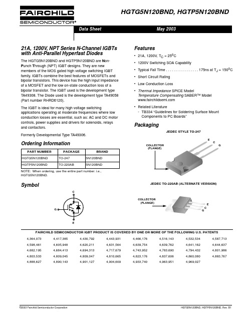
Symbol
C
G
Features
• 21A, 1200V, TC = 25oC • 1200V Switching SOA Capability • Typical Fall Time . . . . . . . . . . . . . . . . 175ns at TJ = 150oC • Short Circuit Rating
元器件交易网
Data Sheet
HGTG5N120BND, HGTP5N120BND
May 2003
21A, 1200V, NPT Series N-Channel IGBTs with Anti-Parallel Hyperfast Diodes
Excel背单词:人教版PEP小学英语3-6年级

70 71 72 73 74 75 76 77 78 79 80 81 82 83 84 85 86 87 88 89 90 91 92 93 94 95 96 97 98 99 100 101 102 103 104 105
B B B B B B B B B B B C C C C C C C C C C C C C C C C C C C C C C C C C
Australia baby bag ball balloon banana bank bathroom bear beautiful because become bed bedroom beef behind best better between big bigger bike bird birthday black blue board boat body book bookstore boots bored bounce boy bread
358 359 360 361 362 363 364 365 366 367 368 369 370 371 372 373 374 375 376 377 378 379 380 381 382 383 384 385 386 387 388 389 390 391 392 393
I I I I I I I I I J J J J J J J J J J K K K K K K K ຫໍສະໝຸດ K K K L L L L L L
Excel背单词:人教版PEP小学英语3-6年级单
序号 1 2 3 4 5 6 7 8 9 10 11 12 13 14 15 16 17 18 19 20 21 22 23 24 25 26 27 28 29 30 31 32 33 首字母 A A A A A A A A A A A A A A A A A A A A A A A A A A A A A A A A A a little a pair of able about accountant active actor actress after school again air air-conditioner all right always and angry another answer the phone ant any apple April are aren’t =are not arm art art room artist assistant at at home August aunt 英文
A101VW01 V3 Spec ver2.1

nf id
en
tia
Storage Temperature:-20
lF
NW
~70
AY
~60
In
te
Update the absolute maximum ratings
rn
al
Explain panel function confirmed in reliability test(Note3).
Us
For SUNWAY Internal Use Only - Provided By bengong On 2014/07/24
AU
O
Co
Note: The content of this specification is subject to change.
nf id
te
rn
© 2010 AU Optronics All Rights Reserved, Do Not Copy.
Product Specification
/0
< >Preliminary Specification >Final Specification <
en
tia
lF
or
SU
NW
AY
In
ALL RIGHTS STRICTLY RESERVED. ANY PORTION OF THIS PAPER SHALL NOT BE REPRODUCED, COPIED, OR TRANSFORMED TO ANY OTHER FORMS WITHOUT PERMISSION FROM AU OPTRONICS CORP.
al
Us
eO
nly
- 1、下载文档前请自行甄别文档内容的完整性,平台不提供额外的编辑、内容补充、找答案等附加服务。
- 2、"仅部分预览"的文档,不可在线预览部分如存在完整性等问题,可反馈申请退款(可完整预览的文档不适用该条件!)。
- 3、如文档侵犯您的权益,请联系客服反馈,我们会尽快为您处理(人工客服工作时间:9:00-18:30)。
_BIS_SR()
是C语言中的本征函数。
其意思是,通过本征函数就可以直接写该状态寄存器中的数值。
其中在_BIS_SR()中,BI 可以理解为BIT 即“位”的意思,而,“S”可以理解为“SET”,而“SR”就是指的事状态寄存器。
这个函数的功能就是对函数所调用的寄存器中的位进行置“1”。
例如:
_BIS_SR(GIE),就是对SR寄存器中的GIE位进行置1,那么也就是打开总中断。
在_BIC_SR()中,BI 可以理解为BIT 即“位”的意思,而“C”就可以理解为“clear”,也就是“清除”的意思,而“SR”就是指的事状态寄存器。
这个函数的意思就是对函数所调用的寄存器中的位进行“清除”,也就是置“0”。
_BIC_SR(GIE),就是对SR寄存器中的GIE位进行置0,那么也就是关闭总中断。
下面就是有这两个函数的430的头文件
/**************************************************
*
* Intrinsic functions for the MSP430 IAR Systems C/C++ Compiler
* provided for backward compatibility with version 1 of the compiler.
*
* Most intrincis functions have been replaced with equivalent
* intrinsic functions that follow the current naming convention.
* However, there are two exceptions:
*
* 1) The intrinsic functions _BIx_SR and _BIx_SR_IRQ are replaced
* with __bix_SR_register and __bix_SR_register_on_exit. The new
* intrinsic functions no longer returns the previous value of the
* status register. You can access that value by using the
* intrinsic function __get_SR_register.
*
* 2) The intrinsic function _BIS_NMI_IE1 has been replaced with the
* #pragma directive bis_nmi_ie1. The reason why this no longer is
* an intrinsic function is that the effect was always performed,
* even if the intrinsic was guarded with, say, an "if"-statement.
*
* Copyright 2002-2003, 2006 IAR Systems. All rights reserved.
*
* $Revision: 4055 $
*
**************************************************/
#ifndef __IN430_H
#define __IN430_H
#ifndef _SYSTEM_BUILD
#pragma system_include
#endif
#include "intrinsics.h"
#pragma language=save
#pragma language=extended
/*
* Deprecated intrinsic functions.
*/
#ifdef __cplusplus
extern "C"
{
#endif
/* Deprecated, please use "__bis_SR_re。