MAX5900LCEUT-T中文资料
MAX213CAI-T中文资料

General DescriptionThe MAX200–MAX211/MAX213 transceivers are designed for RS-232 and V.28 communication inter-faces where ±12V supplies are not available. On-board charge pumps convert the +5V input to the ±10V need-ed for RS-232 output levels. The MAX201 and MAX209operate from +5V and +12V, and contain a +12V to -12V charge-pump voltage converter.The MAX200–MAX211/MAX213 drivers and receivers meet all EIA/TIA-232E and CCITT V.28 specifications at a data rate of 20kbps. The drivers maintain the ±5V EIA/TIA-232E output signal levels at data rates in excess of 120kbps when loaded in accordance with the EIA/TIA-232E specification.The 5µW shutdown mode of the MAX200, MAX205,MAX206, and MAX211 conserves energy in battery-powered systems. The MAX213 has an active-low shut-down and an active-high receiver enable control. Two receivers of the MAX213 are active, allowing ring indica-tor (RI) to be monitored easily using only 75µW power.The MAX211 and MAX213 are available in a 28-pin wide small-outline (SO) package and a 28-pin shrink small-outline (SSOP) package, which occupies only 40% of the area of the SO. The MAX207 is now avail-able in a 24-pin SO package and a 24-pin SSOP. The MAX203 and MAX205 use no external components,and are recommended for applications with limited circuit board space.ApplicationsComputersLaptops, Palmtops, Notebooks Battery-Powered Equipment Hand-Held Equipment Next-Generation Device Features ♦For Low-Cost Applications:MAX221E: ±15kV ESD-Protected, +5V, 1µA, Single RS-232 Transceiver with AutoShutdown™♦For Low-Voltage and Space-Constrained Applications:MAX3222E/MAX3232E/MAX3237E/MAX3241E/MAX3246E: ±15kV ESD-Protected, Down to 10nA,+3.0V to +5.5V, Up to 1Mbps, True RS-232Transceivers (MAX3246E Available in UCSP™Package)♦For Space-Constrained Applications:MAX3228E/MAX3229E: ±15kV ESD-Protected,+2.5V to +5.5V, RS-232 Transceivers in UCSP ♦For Low-Voltage or Data Cable Applications:MAX3380E/MAX3381E: +2.35V TO +5.5V, 1µA,2Tx/2Rx RS-232 Transceivers with ±15kV ESD-Protected I/O and Logic Pins ♦For Low-Power Applications:MAX3224E–MAX3227E/MAX3244E/MAX3245E:±15kV ESD-Protected, 1µA, 1Mbps, +3.0V to+5.5V, RS-232 Transceivers with AutoShutdown Plus™MAX200–MAX211/MAX213+5V , RS-232 Transceivers with 0.1µF External Capacitors ________________________________________________________________Maxim Integrated Products 119-0065; Rev 6; 10/03For pricing, delivery, and ordering information,please contact Maxim/Dallas Direct!at 1-888-629-4642, or visit Maxim’s website at .Ordering Information appears at end of data sheetAutoShutdown, AutoShutdown Plus, and UCSP are trademarks of Maxim Integrated Products, Inc.MAX200–MAX211/MAX213+5V , RS-232 Transceiverswith 0.1µF External Capacitors______________________________________________________________________________________19Ordering Information*Contact factory for dice specifications.M A X 200–M A X 211/M A X 213+5V , RS-232 Transceiverswith 0.1µF External Capacitors Maxim cannot assume responsibility for use of any circuitry other than circuitry entirely embodied in a Maxim product. No circuit patent licenses are implied. Maxim reserves the right to change the circuitry and specifications without notice at any time.20____________________Maxim Integrated Products, 120 San Gabriel Drive, Sunnyvale, CA 94086 408-737-7600©2003 Maxim Integrated ProductsPrinted USAis a registered trademark of Maxim Integrated Products.Package Information(The package drawing(s) in this data sheet may not reflect the most current specifications. For the latest package outline information,go to /packages .)。
MAX4590EAE-T中文资料

General DescriptionThe MAX4580/MAX4590/MAX4600 dual analog switches feature low on-resistance of 1.25Ωmax. On-resistance is matched between switches to 0.25Ωmax and is flat (0.3Ωmax) over the specified signal range. Each switch can handle Rail-to-Rail ®analog signals. The off-leakage current is only 2.5nA max at +85°C. These analog switches are ideal in low-distortion applications and are the preferred solution over mechanical relays in automat-ic test equipment or applications where current switching is required. They have low power requirements, require less board space, and are more reliable than mechanical relays.The MAX4580 has two NC (normally closed) switches,the MAX4590 has two NO (normally open) switches,and the MAX4600 has one NC (normally closed) and one NO (normally open) switch.These switches operate from a +4.5V to +36V single supply or from ±4.5V to ±20V dual supplies. All digital inputs have +0.8V and +2.4V logic thresholds, ensuring TTL/CMOS-logic compatibility when using a +12V sin-gle supply or ±15V dual supplies.ApplicationsReed Relay Replacement Test EquipmentCommunication Systems PBX, PABX SystemsFeatureso Low On-Resistance (1.25Ωmax)o Guaranteed R ON Match Between Channels (0.25Ωmax)o Guaranteed R ON Flatness Over Specified Signal Range (0.3Ωmax)o Rail-to-Rail Signal Handlingo Guaranteed ESD Protection >2kV per Method 3015.7o Single-Supply Operation: +4.5V to +36V Dual-Supply Operation: ±4.5V to ±20V o TTL/CMOS-Compatible Control InputsMAX4580/MAX4590/MAX46001.25Ω, Dual SPST,CMOS Analog Switches________________________________________________________________Maxim Integrated Products119-1394; Rev 1; 6/03Ordering Information continued at end of data sheet.Rail-to-Rail is a registered trademark of Nippon Motorola, Ltd.Pin Configurations/Functional Diagrams/Truth TablesOrdering InformationFor pricing, delivery, and ordering information,please contact Maxim/Dallas Direct!at 1-888-629-4642, or visit Maxim’s website at .M A X 4580/M A X 4590/M A X 46001.25Ω, Dual SPST,CMOS Analog Switches 2_______________________________________________________________________________________ABSOLUTE MAXIMUM RATINGSStresses beyond those listed under “Absolute Maximum Ratings” may cause permanent damage to the device. These are stress ratings only, and functional operation of the device at these or any other conditions beyond those indicated in the operational sections of the specifications is not implied. Exposure to absolute maximum rating conditions for extended periods may affect device reliability.V+ to GND..............................................................-0.3V to +44V V- to GND...............................................................+0.3V to -44V V+ to V-...................................................................-0.3V to +44V V L to GND....................................................-0.3V to (V+ + 0.3V)All Other Pins to GND (Note 1) ...........(V- - 0.3V) to (V+ + 0.3V)Continuous Current (COM_, NO_, NC_) .......................±200mA Peak Current (COM_, NO_, NC_)(pulsed at 1ms, 10% duty cycle) ..............................±300mAContinuous Power Dissipation (T A = +70°C)16 SSOP (derate 7.1mW/°C above +70°C).................571mW 16 Wide SO (derate 9.52mW/°C above +70°C) ..........762mW 16 Plastic DIP (derate 10.53mW/°C above +70°C).....842mW Operating Temperature RangesMAX4_ _0C_E ....................................................0°C to +70°C MAX4_ _0E_E ..................................................-40°C to +85°C Storage Temperature Range ...........................-65°C to +160°C Lead Temperature (soldering, 10sec) ............................+300°CELECTRICAL CHARACTERISTICS–Dual Supplies(V+ = +15V, V- = -15V, V L = +5V, V IN_H = +2.4V, V IN_L = +0.8V, T A = T MIN to T MAX , unless otherwise noted. Typical values are at T A = +25°C.)Note 1:Signals on NC_, NO_, COM_, or IN_ exceeding V+ or V- are clamped by internal diodes. Limit forward diode current tomaximum current rating.ELECTRICAL CHARACTERISTICS–Dual Supplies (continued)MAX4580/MAX4590/MAX46001.25Ω, Dual SPST,CMOS Analog Switches (V+ = +15V, V- = -15V, V L= +5V, V IN_H= +2.4V, V IN_L= +0.8V, T A = T MIN to T MAX, unless otherwise noted. Typical values are atT A= +25°C.)_______________________________________________________________________________________3M A X 4580/M A X 4590/M A X 46001.25Ω, Dual SPST,CMOS Analog Switches 4_______________________________________________________________________________________ELECTRICAL CHARACTERISTICS–Single Supply(V+ = +12V, V- = 0, V L = +5V, V INH = 2.4V, V INL = 0.8V, T A = T MIN to T MAX , unless otherwise noted. Typical values are at T = +25°C.)MAX4580/MAX4590/MAX46001.25Ω, Dual SPST,CMOS Analog Switches_______________________________________________________________________________________5ELECTRICAL CHARACTERISTICS—Single Supply (continued)(V+ = +12V, V- = 0, V L = +5V, V IN_H = 2.4V, V IN_L = 0.8V, T A = T MIN to T MAX , unless otherwise noted. Typical values are at T A = +25°C.)Note 2:The algebraic convention, where the most negative value is a minimum and the most positive value a maximum, is used inthis data sheet.Note 3:Guaranteed by design.Note 4:∆R ON = R ON(MAX)- R ON(MIN).Note 5:Flatness is defined as the difference between the maximum and minimum value of on-resistance as measured over thespecified analog signal range.Note 6:Leakage parameters are 100% tested at maximum-rated hot temperature and guaranteed by correlation at +25°C.Note 7:Off-isolation = 20 log 10[V COM / (V NC or V NO )], V COM = output, V NC or V NO = input to off switch.Note 8:Between any two switches.Note 9:Leakage testing at single supply is guaranteed by testing with dual supplies.0.51.01.52.02.5-20-12-8-16-448121620ON-RESISTANCE vs. V COM(DUAL SUPPLIES)V COM (V)R O N (Ω)ON-RESISTANCE vs. V COMAND TEMPERATURE (DUAL SUPPLIES)V COM (V)R O N (Ω)129-12-9-63-360.50.60.70.80.91.01.11.20.4-1515ON-RESISTANCE vs. V COM(SINGLE SUPPLY)V COM (V)R O N (Ω)2220181614121086421234524Typical Operating Characteristics(Circuit of Figure 1, T A = +25°C, unless otherwise noted.)Typical Operating Characteristics (continued)(Circuit of Figure 1, T A = +25°C, unless otherwise noted.)M A X 4580/M A X 4590/M A X 46001.25Ω, Dual SPST,CMOS Analog Switches 6_______________________________________________________________________________________ON-RESISTANCE vs. V COMAND TEMPERATURE (SINGLE SUPPLY)V COM (V)R O N (Ω)11108923456710.250.500.751.001.251.501.752.002.2500120.0010.010.11100101000-4020-20406080100POWER-SUPPLY CURRENTvs. TEMPERATURETEMPERATURE (°C)I +, I - (n A )10,0000.0010.01110-4020-20406080100ON/OFF-LEAKAGE vs. TEMPERATURETEMPERATURE (°C)L E A K A G E (n A )-500-3000200400-400-100100300500-15-50-10515CHARGE INJECTIONvs. V COMV COM (V)Q (p C )10-2000-1000.011100.1100-80FREQUENCY (MHz)L O S S (d B )P H A S E (d e g r e e s )-60-40-20-90-70-50-30-10+180-720-540-360-1800-630-450-270-90+9050100150250300-4010-15356085TURN-ON/TURN-OFF TIME vs. TEMPERATURETEMPERATURE (°C)t O N , t O F F (n s )MAX4580/MAX4590/MAX46001.25Ω, Dual SPST,CMOS Analog Switches_______________________________________________________________________________________7801202001602402801012111314151617181920TURN-ON/TURN-OFF TIME vs. SUPPLY VOLTAGEV+, V- (V)t O N , t O F F (n s )Typical Operating Characteristics (continued)(Circuit of Figure 1, T A = +25°C, unless otherwise noted.)TURN-ON/TURN-OFF TIME vs. V COMV COM (V)t O N , t O F F (n s )8642-2-4-6-8120140160180200220100-1010Pin DescriptionM A X 4580/M A X 4590/M A X 46001.25Ω, Dual SPST,CMOS Analog Switches8__________________________________________________________________________________________________Applications InformationOvervoltage ProtectionProper power-supply sequencing is recommended for all CMOS devices. Do not exceed the absolute maxi-mum ratings, because stresses beyond the listed rat-ings can cause permanent damage to the devices.Always sequence V+ on first, then V-, followed by the logic inputs, NO, or COM. If power-supply sequencing is not possible, add two small signal diodes (D1, D2) in series with supply pins for overvoltage protection (Figure 1). Adding diodes reduces the analog signal range to one diode drop below V+ and one diode drop above V-, but does not affect the devices’ low switch resistance and low leakage characteristics. Device operation is unchanged, and the difference between V+and V- should not exceed 44V. These protection diodes are not recommended when using a single supply.Figure 1. Overvoltage Protection Using External Blocking DiodesFigure 2. Switching-Time Test CircuitMAX4580/MAX4590/MAX46001.25Ω, Dual SPST,CMOS Analog Switches_______________________________________________________________________________________9Figure 4. Off-Isolation Test Circuit Figure 5. Crosstalk Test CircuitM A X 4580/M A X 4590/M A X 46001.25Ω, Dual SPST,CMOS Analog Switches 10______________________________________________________________________________________Ordering Information (continued)___________________Chip InformationTRANSISTOR COUNT: 100Figure 6. Switch Off-Capacitance Test CircuitFigure 7. Switch On-Capacitance Test CircuitPackage InformationMAX4580/MAX4590/MAX46001.25Ω, Dual SPST,CMOS Analog Switches (The package drawing(s) in this data sheet may not reflect the most current specifications. For the latest package outline informationgo to /packages.) Array______________________________________________________________________________________11M A X 4580/M A X 4590/M A X 46001.25Ω, Dual SPST,CMOS Analog Switches S O I C W .E P SPackage Information (continued)(The package drawing(s) in this data sheet may not reflect the most current specifications. For the latest package outline information go to /packages .)Ma xim ca nnot a ssume responsibility for use of a ny circuitry other tha n circuitry entirely embodied in a Ma xim product. No circuit pa tent licenses a re implied. Maxim reserves the right to change the circuitry and specifications without notice at any time.12____________________Maxim Integrated Products, 120 San Gabriel Drive, Sunnyvale, CA 94086 408-737-7600©2003 Maxim Integrated ProductsPrinted USAis a registered trademark of Maxim Integrated Products.。
MAX809SN160T1资料
MAX809 Series,MAX810 SeriesVery Low Supply Current 3-Pin Microprocessor Reset MonitorsThe MAX809 and MAX810 are cost–effective system supervisor circuits designed to monitor V CC in digital systems and provide a reset signal to the host processor when necessary. No external components are required.The reset output is driven active within 10 µsec of V CC falling through the reset voltage threshold. Reset is maintained active for a minimum of 140 msec after V CC rises above the reset threshold. The MAX810 has an active–high RESET output while the MAX809 has an active–low RESET output. The output of the MAX809 is guaranteed valid down to V CC = 1.0 V. Both devices are available in a SOT–23 package.The MAX809/810 are optimized to reject fast transient glitches on the V CC line. Low supply current of 1.0 µA (V CC= 3.2 V) makes these devices suitable for battery powered applications.Features•Precision V CC Monitor for 2.5 V, 3.0 V, 3.3 V, and 5.0 V Supplies •Precision Monitoring V oltages from 1.6 V to 4.9 V Availablein 100 mV Steps•140 msec Guaranteed Minimum RESET Output Duration •RESET Output Guaranteed to V CC = 1.0 V•Low Supply Current•V CC Transient Immunity•Small SOT–23 Package•No External Components•Wide Operating Temperature: –40°C to 105°CTypical Applications•Computers•Embedded Systems•Battery Powered Equipment•Critical µP Power Supply MonitoringV CCFigure 1. Typical Application DiagramDevice Package ShippingORDERING INFORMATIONMAX809xTR SOT–233000 Tape/Reel MAX809SNxxxT1SOT–233000 Tape/Reel NOTE:*SOT–23 is equivalent to JEDEC (TO–236) **RESET is for MAX809***RESET is for MAX810SOT–23(TO–236)CASE 318PIN CONFIGURATION312V CCGNDRESET**SOT–23*(Top View)xx, xxx= Specific Device Codem= Date Codey= Yearw= Work WeekMARKINGDIAGRAMS32xxxm1(RESET)***MAX810xTR SOT–233000 Tape/ReelSee general marking information in the device marking section on page 8 of this data sheet.DEVICE MARKING INFORMATION NOTE: The “x” and “xxx” denotes a suffix for V cc voltage threshold options – see page 8 for more details.32xxyw1See specific device markinginformation on page 8.PIN DESCRIPTIONABSOLUTE MAXIMUM RATINGS* (Note 1)1.This device series contains ESD protection and exceeds the following tests:Human Body Model 2000 V per MIL–STD–883, Method 3015. Machine Model Method 350 V.2.The maximum package power dissipation limit must not be exceeded.P D +T J(max)*T Aq JAwith T J(max) = 150°C ELECTRICAL CHARACTERISTICS T A = –40°C to +105°C unless otherwise noted. Typical values are at T A = +25°C. (Note 3)The following data is given for MAX809 threshold levels: 1.60 V, 2.32 V, 2.93 V, 4.63 V and 4.90 V.AELECTRICAL CHARACTERISTICS(continued) T A = –40°C to +105°C unless otherwise noted. Typical values are at T A = +25°C. (Note 4) The following data is given for MAX809 threshold levels: 1.60 V, 2.32 V, 2.93 V, 4.63 V and 4.90 V.A5.Contact your ON Semiconductor sales representative for other threshold voltage options.ELECTRICAL CHARACTERISTICS (V CC = Full Range, T A = –40°C to +85°C unless otherwise noted. Typical values are at T A = +25°C, V CC = 5.0 V for L/M/J, 3.3 V for T/S, 3.0 V for R) (Note 6) The following data is given for MAX809 threshold levels: 2.63 V, 3.08 V, 4.00 V and 4.38 V; MAX810 threshold levels: 2.63 V, 2.93 V, 3.08 V, 4.38 V and 4.63 V.AAPPLICATIONS INFORMATIONV CC Transient RejectionThe MAX809 provides accurate V CC monitoring and reset timing during power–up, power–down, and brownout/sag conditions, and rejects negative–going transients (glitches)on the power supply line. Figure 2 shows the maximum transient duration vs. maximum negative excursion (overdrive) for glitch rejection. Any combination of duration and overdrive which lies under the curve will not generate a reset signal. Combinations above the curve are detected as a brownout or power–down. Typically, transient that goes 100 mV below the reset threshold and lasts 5 µs or less will not cause a reset pulse. Transient immunity can be improved by adding a capacitor in close proximity to the V CC pin of the MAX809.Figure 2. Maximum Transient Duration vs. Overdrivefor Glitch Rejection at 25°CV CC10.010080110.060.0M A X I M U M T R A N S I E N T D U R A T I O N (µs e c )20120RESET COMPARATOR OVERDRIVE (mV)160.06040RESET Signal Integrity During Power–DownThe MAX809 RESET output is valid to V CC = 1.0 V .Below this voltage the output becomes an “open circuit” and does not sink current. This means CMOS logic inputs to the µP will be floating at an undetermined voltage. Most digital systems are completely shutdown well above this voltage.However, in situations where RESET must be maintainedvalid to V CC = 0 V , a pull–down resistor must be connected from RESET to ground to discharge stray capacitances and hold the output low (Figure 3). This resistor value, though not critical, should be chosen such that it does not appreciably load RESET under normal operation (100 k W will be suitable for most applications).Figure 3. Ensuring RESET Valid to V CC = 0 VProcessors With Bidirectional I/O PinsSome µP’s (such as Motorola 68HC11) have bi–directional reset pins. Depending on the current drive capability of the processor pin, an indeterminate logic level may result if there is a logic conflict. This can be avoided by adding a 4.7 k W resistor in series with the output of the MAX809 (Figure 4). If there are other components in the system which require a reset signal, they should be buffered so as not to load the reset line. If the other components are required to follow the reset I/O of the µP, the buffer should be connected as shown with the solid line.Figure 4. Interfacing to Bidirectional Reset I/OBUFFERED RESETThe following data is given for MAX809 threshold levels: 1.60 V, 2.32 V, 2.93 V, 4.63 V and 4.90 V.1.10S U P P L Y C U R R E N T I N M I C R O A M PTEMPERATURE (°C)N O R M A L I Z E D P O W E R –U P R E S E T T I M E O U T–404020–206080Figure 7. Normalized Power–Up Reset vs.Temperature Figure 8. Normalized Reset Threshold Voltagevs. TemperatureTEMPERATURE (°C)–404020–206080The following data is given for MAX809 threshold levels: 2.63 V, 3.08 V, 4.00 V and 4.38 V;MAX810 threshold levels: 2.63 V, 2.93 V, 3.08 V, 4.38 V and 4.63 V.S U P P L Y C U R R E N T ( A )m 040206080100P O W E R -D O W N R E S E T D E L A Y ( s e c )m TEMPERATURE (C °)-40-200204085Figure 13. Power–Up Reset Timeout vs.Temperature TEMPERATURE (C °)-40-20020406085225235230240245250P O W E R -U P R E S E T T I M E O U T (m s e c )60Figure 14. Normalized Reset Threshold vs.TemperatureTAPING FORMComponent Taping Orientation for 3L SOT–23 (JEDEC–236) Devices(Mark Right Side Up)SOT–23Package Carrier Width (W)Pitch (P)Part Per Full ReelReel Size 8 mm4 mm30007 inchesTape & Reel Specifications TableMARKING AND THRESHOLD INFORMATIONm = Date Codey = Yearw = Work WeekPACKAGE DIMENSIONSSOT–23PLASTIC PACKAGE (TO–236)CASE 318–08ISSUE AHNOTES:1.DIMENSIONING AND TOLERANCING PER ANSI Y14.5M, 1982.2.CONTROLLING DIMENSION: INCH.3.MAXIMUM LEAD THICKNESS INCLUDES LEADNotesNotes11ON Semiconductor and are trademarks of Semiconductor Components Industries, LLC (SCILLC). SCILLC reserves the right to make changes without further notice to any products herein. SCILLC makes no warranty, representation or guarantee regarding the suitability of its products for any particular purpose, nor does SCILLC assume any liability arising out of the application or use of any product or circuit, and specifically disclaims any and all liability, including without limitation special, consequential or incidental damages. “Typical” parameters which may be provided in SCILLC data sheets and/or specifications can and do vary in different applications and actual performance may vary over time. All operating parameters, including “Typicals” must be validated for each customer application by customer’s technical experts. SCILLC does not convey any license under its patent rights nor the rights of others.SCILLC products are not designed, intended, or authorized for use as components in systems intended for surgical implant into the body, or other applications intended to support or sustain life, or for any other application in which the failure of the SCILLC product could create a situation where personal injury or death may occur. Should Buyer purchase or use SCILLC products for any such unintended or unauthorized application, Buyer shall indemnify and hold SCILLC and its officers, employees, subsidiaries, affiliates, and distributors harmless against all claims, costs, damages, and expenses, and reasonable attorney fees arising out of, directly or indirectly, any claim of personal injury or death associated with such unintended or unauthorized use, even if such claim alleges that SCILLC was negligent regarding the design or manufacture of the part. SCILLC is an Equal Opportunity/Affirmative Action Employer. PUBLICATION ORDERING INFORMATIONJAPAN: ON Semiconductor, Japan Customer Focus Center4–32–1 Nishi–Gotanda, Shinagawa–ku, Tokyo, Japan 141–0031Phone: 81–3–5740–2700Email: r14525@。
林肯电气贝斯特CITOCUT 25i操作手册说明书

Electromagnetic Compatibility (EMC)01/11 This machine has been designed in accordance with all relevant directives and standards. However, it may still generate electromagnetic disturbances that can affect other systems like telecommunications (telephone, radio, and television) or other safety systems. These disturbances can cause safety problems in the affected systems. Read and understand this section to eliminate or reduce the amount of electromagnetic disturbance generated by this machine.This machine has been designed to operate in an industrial area. The operator must install and operate thisequipment as described in this manual. If any electromagnetic disturbances are detected the operator must putin place corrective actions to eliminate these disturbances with, if necessary, assistance from Lincoln Electric.This machine is not in accordance with IEC 61000-3-12. If it is powered by a low voltage public distribution network in the connection responsibility of the installer or user of equipment, consultation, if necessary, with the electricity service distributor.Before installing the machine, the operator must check the work area for any devices that may malfunction because of electromagnetic disturbances. Consider the following.∙Input and output cables, control cables, and telephone cables that are in or adjacent to the work area and the machine. ∙Radio and/or television transmitters and receivers. Computers or computer controlled equipment.∙Safety and control equipment for industrial processes. Equipment for calibration and measurement.∙Personal medical devices like pacemakers and hearing aids.∙Check the electromagnetic immunity for equipment operating in or near the work area. The operator must be sure that all equipment in the area is compatible. This may require additional protection measures.∙The dimensions of the work area to consider will depend on the construction of the area and other activities that are taking place.Consider the following guidelines to reduce electromagnetic emissions from the machine.∙Connect the machine to the input supply according to this manual. If disturbances occur if may be necessary to take additional precautions such as filtering the input supply.∙The output cables should be kept as short as possible and should be positioned together. If possible connect the work piece to ground in order to reduce the electromagnetic emissions. The operator must check that connecting the work piece to ground does not cause problems or unsafe operating conditions for personnel and equipment.∙Shielding of cables in the work area can reduce electromagnetic emissions. This may be necessary for special applications.due to conducted as well as radio-frequency disturbances.Safety01/11WARNINGThis equipment must be used by qualified personnel. Be sure that all installation, operation, maintenance and repair procedures are performed only by qualified person. Read and understand this manual before operating this equipment. Failure to follow the instructions in this manual could cause serious personal injury, loss of life, or damage to this equipment. Read and understand the following explanations of the warning symbols. Lincoln Electric is not responsible for damages caused by improper installation, improper care or abnormal operation.Do not remove or paint over (cover) the label.SAFETY MARK: This equipment is suitable for supplying power for cutting operations carried out in anenvironment with increased hazard of electric shock.The manufacturer reserves the right to make changes and/or improvements in design without upgrade at the same time the operator’s manual.Installation and Operator InstructionsRead this entire section before installation or operation of the machine.Location and EnvironmentThis machine can operate in harsh environments. However, it is important that simple preventative measures are followed to assure long life and reliable operation:∙Do not place or operate this machine on a surface with an incline greater than 15° from horizontal.∙Do not use this machine for pipe thawing.∙This machine must be located where there is free circulation of clean air without restrictions for air movement to and from the air vents. Do not cover the machine with paper, cloth or rags when switched on.∙Dirt and dust that can be drawn into the machine should be kept to a minimum.∙This machine has a protection rating of IP23S. Keep it dry when possible and do not place it on wet ground or in puddles.∙Locate the machine away from radio controlled machinery. Normal operation may adversely affect the operation of nearby radio controlled machinery, which may result in injury or equipment damage.Read the section on electromagnetic compatibility in this manual.∙Do not operate in areas with an ambient temperature greater than 40°C.Duty CycleThe duty cycle of a plasma machine is the percentage of time in a 10 minute cycle at which the operator can operate the machine at rated cutting current.Example: 35% duty cycle means that is possible cut for 3,5 minutes, then the machine stops for 6,5minutes.Refer to the Technical Specification section for more information about the machine rated duty cycles.Input Supply ConnectionCheck the input voltage, phase, and frequency supplied to this machine before turning it on. The allowable input voltage is indicated in the technical specification section of this manual and on the rating plate of the machine. Be sure that the machine is grounded.Make sure the amount of power available from the input connection is adequate for normal operation of the machine. The fuse rating and cable sizes are both indicated in the technical specification section of this manual. The machines:∙CITOCUT 25iare designed to operate on engine driven generators as long as the auxiliary can supply adequate voltage, frequency and power as indicated in the "Technical Specification" section of this manual. The auxiliary supply of the generator must also meet the following conditions:∙Vac peak voltage: below 410V.∙Vac frequency: 50Hz.∙RMS voltage of the AC waveform: 230Vac ± 10%.It is important to check these conditions because many engine driven generators produce high voltage spikes. Operation of this machine on engine driven generators not conforming to these conditions is not recommended and may damage the machine.Output ConnectionsWARNINGUse ONLY the torch supplied with this machine. For areplacement refer to the Maintenance section of this manual.WARNINGAlways turn OFF the machine when working on the torch.WARNINGDo not remove the work clamp during cutting, plasma cutting generates high voltages that can kill.WARNINGOpen Circuit Voltage U0 > 100VDC. For more information refer to the Technical Specification section. This machine is sent from the factory with a cutting torch and work clamp installed. The work clamp must be securely connected to the work piece. If the work piece is painted or extremely dirty it may be necessary to expose the bare metal in order to make a good electrical connection.Built-In CompressorThis machine has a built-in compressor that allow to operates in areas where an external primary air is not available. Only an electrical mains supply is necessary!Controls and Operational Features CITOCUT 25i front command panel.Commands descriptions:A. Output Current Knob: Potentiometer used to set theoutput current used during cutting. Refer to the Technical Specification section for more information about the machine rated current range.Air Purge: The Output Current Knob completely rotated counterclockwise enables the air purge function. A 5 minutes timeout stops the purge function; this happens only if the Output Current Knob remains in the purge mode for a long time.B. Power ON/OFF green LED: It lights up when themachine is ON.C. Output red LED: See meanings in the following table.D. Thermal yellow LED: See meanings in the followingtable.LEDs MeaningOutput(Red)Thermal(Yellow)On Off The cutting torch is energized.On OnPart in place error: the retaining capis not properly screwed.To restore the machine:∙Screw firmly the torch retainingcap.∙Wait for 5seconds; during thistime the Output and ThermalLEDs blinks alternately.∙After 5seconds the machine isautomatically restored and readyto operate.Off OnThe machine is overheated and theoutput has been disabled. Thisusually occurs when the duty cycleof the machine has been exceeded.Leave the machine On to allow theinternal components to cool. Whenthe thermal LED turns off, normaloperation is again possible.Off BlinkMains undervoltage or overvoltageerror: the machine is disabled.When the mains return in thecorrect range, the machine restartautomatically.Blink Off Low air pressure error.To check / adjust the air pressure(see recommended values in theTecnical Specifications of thismanual):∙Put the machine in Purge mode[A].∙ Check and adjust the airpressure through themanometer and air pressureregulator knob [F].∙If necessary, check and adjustalso the inlet air pressurethrough the commands of theexternal compressor.E. Internal / External air selection :This switch determine the air supply. With the “InCompr” position selected, the machine operatesthrough the built-in compressor. With the “Ext Air”position selected, the internal compressor iscompletely disabled and the machine operatesthrough an external air supply hose connected to theproper air inlet connection placed on the machine rearside.WARNINGIf operate with external air, be sure to select the “Ext Air” switch position in order to completely disable the built-in compressor. Otherwise the compressor may be damagedby the probable greater pressure of the external air.F. Air Pressure Gauge and Regulator Knob :Allow to regulate and monitoring the air pressure.G. Fan: Provides machine cooling. It is switched ONwith the machine and continues to run till the machine is turned OFF.H. Power Switch: It turns ON / OFF the input power tothe machine.I. Input cable: Connect it to the mains.J. Air Inlet : If the “Ext Air” operating mode is selected, connect here the hose carrying the air to the machine.WARNINGA clean, dry air must be supplied to the machine. A pressure setting above 7.5bar could damage the torch. Failure to observe these precautions could result in excessive operating temperatures or damage to the torch. Cutting ProcessThe air plasma cutting process uses air as primary cutting gas and as torch cooling gas.The air is provided by the built-in compressor with a pressure of 3.5bar (approximate value).The Citicut 25i can reach the best cutting performances operates also with external air; in this case the air pressure is limited by a pressure regulator [F], set at factory at 5.0bar. In case to adjust the air pressure, put the machine in Purge mode [A].The pilot arc is struck as follow:∙“In Compr” operating mode:The torch button enables the built-in compressorthat provide the air flow to the torch. Releasing thetorch button the cutting process is stopped, but thecompressor continues to run for the post-flowstage.∙“Ext Air” operating mode: the torch button energize an electrovalve (solenoid valve). Thisvalve lets the air flow during the cutting and thepost-flow stages.The design concept at the basis of these power sources is to have available a current which remains constant at the set value, independently from the length of the plasma arc. When preparing to cut, make sure you have all materials needed to complete the job and have taken all safety precautions. Install the machine as instructed in this manual and remember to attach the work clamp to the work piece.∙Turn ON the Power Switch [H] placed on the back of the machine; the LED [B] on the front panel will turn ON. The unit is now ready to operate.∙Check that the primary air is available through the Air Purge function [A].∙Set the desired current value with the Output Current[A] knob.To start the cutting process just press the torch button, making sure you are not aiming the torch air blow towards people or foreign objects. During the cutting process it is possible to hold the torch away from the work piece for an extended period of time.To piercing the work piece, lower thetorch onto the metal at a 30° angleaway from the operator. This will blowthe dross (melted metal) away fromthe torch tip.Slowly rotate the torch to the verticalposition as the arc becomes deeper.Once the work piece is pierced normalcutting can occur.Keep moving while cuttingand cut at a steady speed sothat the arc leg is 10° to 20°behind the travel direction.Use a 5° to 15° leading anglein the direction of the cut.Once the cutting process isterminated releasing off thetorch button will cause theplasma arc to be turned off;the air flow will continue forapproximately 20sec. (post-flow) to allow the cooling down of the torch.MaintenanceWARNINGFor any maintenance or repair operations it is recommended to contact the nearest technical service center or Lincoln Electric. Maintenance or repairs performed by unauthorized service centers or personnel will null and void the manufacturers warranty.The frequency of the maintenance operations may vary in accordance with the working environment. Any noticeable damage should be reported immediately.∙Check cables and connections integrity. Replace, if necessary.∙Regularly clean the torch head, check its consumables and if necessary replace them.WARNINGRefer to the torch instructions before changing or servicing the torch.∙Keep clean the machine. Use a soft dry cloth to clean the enclosing case, especially the airflow inlet / outlet louvers.∙Regularly clean the compressor air inlet filter.WARNINGDo not open this machine and do not introduce anything into its openings. Power supply must be disconnected from the machine before maintenance and service. After each repair, perform proper tests to check safety requirements.Cutting SpeedThe cutting speed is a function of:∙ Thickness and of material to be cut.∙ Value of set current. The current setting affects thequality of the cut edge.∙ Geometrical shape of the cut (whether straight orcurved). In order to provide indications on the most suitable setting, the following table was established, based on tests performed on an automatic test-bench; the best results however can only be achieved from direct experience by the operator in his actual working conditions.CITOCUT 25i (internal air) CITOCUT 25i (external air) Speed (cm/min.)Speed (cm/min.)T h i c k n e s sC u r r e n t (A )M I L D S T E E LA L U M I N U MS T A I N L E S S S T E E LC u r r e n t (A )M I L D S T E E L A L U M I N U M S T A I N L E S S S T E E L 4 mm 25 147 94 77.7 25 179 122 112.8 5 mm 25 108 86 59 25 131 104 90 6 mm 25 73 68 47 25 80.6 81.6 70 ¼” 25 55 58 43 25 67 70 62 8 mm --- --- --- --- --- --- --- --- ⅜” 25 10 --- 23 25 12 --- 3010 mm 25 --- --- 20.4 25 --- --- 23.6 11 mm --- --- --- --- --- --- --- --- ½” 25 --- --- 11 25 --- --- 12 15 mm------------------------ ¾” --- --- --- --- --- --- --- ---Customer Assistance PolicyThe business of The Lincoln Electric Company is manufacturing and selling high quality welding equipment, consumables, and cutting equipment. Our challenge is to meet the needs of our customers and to exceed their expectations. On occasion, purchasers may ask Lincoln Electric for advice or information about their use of our products. We respond to our customers based on the best information in our possession at that time. Lincoln Electric is not in a position to warrant or guarantee such advice, and assumes no liability, with respect to such information or advice. We expressly disclaim any warranty of any kind, including any warranty of fitness for any customer’s particular purpose, with respect to such information or advice. As a matter of practical consideration, we also cannot assume any responsibility for updating or correcting any such information or advice once it has been given, nor does the provision of information or advice create, expand or alter any warranty with respect to the sale of our productsLincoln Electric is a responsive manufacturer, but the selection and use of specific products sold by Lincoln Electric is solely within the control of, and remains the sole responsibility of the customer. Many variables beyond the control of Lincoln Electric affect the results obtained in applying these types of fabrication methods and service requirements.Subject to Change – This information is accurate to the best of our knowledge at the time of printing. Please refer to for any updated information.WEEESpare Parts12/05 Part List reading instructions∙Do not use this part list for a machine if its code number is not listed. Contact the Lincoln Electric Service Department for any code number not listed.∙Use the illustration of assembly page and the table below to determine where the part is located for your particular code machine.∙Use only the parts marked "X" in the column under the heading number called for in the assembly page (# indicate a change in this printing).First, read the Part List reading instructions above, then refer to the "Spare Part" manual supplied with the machine, that contains a picture-descriptive part number cross-reference.REACh11/19 Communication in accordance with Article 33.1 of Regulation (EC) No 1907/2006 – REACh.Some parts inside this product contain:Bisphenol A, BPA, EC 201-245-8, CAS 80-05-7Cadmium, EC 231-152-8, CAS 7440-43-9Lead, EC 231-100-4, CAS 7439-92-1Phenol, 4-nonyl-, branched, EC 284-325-5, CAS 84852-15-3in more than 0,1% w/w in homogeneous material. These substances are included in the “Candidate List of Substances of Very High Concern for Authorisation” of REACh.Your particular product may contain one or more of the listed substances.Instructions for safe use:∙use according to Manufacturer instructions, wash hands after use;∙keep out of reach of children, do not put in mouth,∙dispose in accordance with local regulations.Authorized Service Shops Location09/16 ∙The purchaser must contact Lincoln Electric or Authorized Service Facility about any defect claimed under warranty period.∙Contact your local Sales Representative for assistance in locating the nearest Authorized Service Facility. Electrical SchematicRefer to the "Spare Part" manual supplied with the machine.。
英特尔联合百度,共同开发Nervana神经网络训练处理器
置很简单,即使是设置较大的5.1和7.1系统也只需几分钟。
(来自W i SA协会)儒卓力提供具有最高功率密度和效率的英飞凌O pti M O S T M功率M O S F ET英飞凌O p ti M O S TM3和5同类最佳(Bi C)功率M O S F E T采用节省空间的S up e r S O8封装,与先前型号相比,具有更高的功率密度和稳健性,从而降低系统成本和提升整体性能。
由于具有最低的导通电阻,这些Bi C M O S F E T 能够以良好的性价比降低损耗。
此外,通管壳的较低热阻提供了出色的散热性能,从而带来更低的满载运作温度。
较低的反向恢复电荷通过显著减小电压过冲来提高系统可靠性,从而最大限度地减少对缓冲电路的需求,同时也减少了工程成本和工作量。
(来自儒卓力)市场要闻英特尔联合百度,共同开发N e r v ana神经网络训练处理器在近日举行的百度AI开发者大会上,英特尔公司副总裁兼人工智能产品事业部总经理Na v ee n Ra o 宣布,英特尔正与百度合作开发英特尔誖Ne r v a n a TM 神经网络训练处理器(NNP-T)。
这一合作包括全新定制化加速器,以实现极速训练深度学习模型的目的。
英特尔在人工智能方面提供优越的硬件选择,并通过软件来最大化释放硬件的性能,从而帮助客户无论数据多么复杂或位于哪里都可以自如运行AI应用。
此次NNP-T是一类全新开发的高效深度学习系统硬件,能够加速大规模的分散训练。
与百度的密切合作能够确保英特尔开发部门始终紧跟客户对训练硬件的最新需求。
此外,鉴于数据安全对于用户极其重要,英特尔还与百度共同致力于打造基于英特尔软件保护扩展(SG X)技术的M esa T EE*———内存安全功能即服务(F aa S)计算框架。
(来自英特尔)Arm与中国联通成功部署物联网设备管理平台解决方案日前,A r m宣布与中国联通旗下联通物联网有限责任公司(物联网公司)的合作取得了最新进展,A r m已成功部署基于A r m Peli on设备管理平台与M b ed O S操作系统所打造的全新物联网平台,加速推进和完善中国物联网生态发展。
MAX2605-MAX2609中文资料
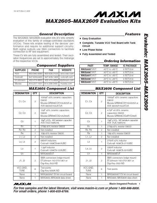
General DescriptionThe MAX2605–MAX2609 evaluation kits (EV kits) simplify evaluation of this family of voltage-controlled oscillators (VCOs). These kits enable testing of the devices’ per-formance and require no additional support circuitry.Both signal outputs use SMA connectors to facilitate connection to RF test equipment.These EV kits are fully assembled and tested. Their oscil-lation frequencies are set to approximately the midrange of the respective VCOs.Featureso Easy Evaluationo Complete, Tunable VCO Test Board with Tank Circuit o Low Phase Noiseo Fully Assembled and TestedEvaluate: MAX2605–MAX2609MAX2605–MAX2609 Evaluation Kits19-1673 Rev 0; 9/00Ordering InformationComponent SuppliersFor free samples and the latest literature, visit or phone 1-800-998-8800.For small orders, phone 1-800-835-8769.MAX2606 Component ListMAX2605 Component ListE v a l u a t e : M A X 2605–M A X 2609MAX2605–MAX2609 Evaluation Kits 2_______________________________________________________________________________________Quick StartThe MAX2605–MAX2609 evaluation kits are fully assembled and factory tested. Follow the instructions in the Connections a nd Setup section for proper device evaluation.Test Equipment Required•Low-noise power supplies (these are recommended for oscillator noise measurement). Noise or ripple will frequency-modulate the oscillator and cause spectral spreading. Batteries can be used in place of power supplies, if necessary.– Use a DC power supply capable of supplying +2.7V to +5.5V. Alternatively, use two or three 1.5V batteries.– Use a DC power supply capable of supplying +0.4V to +2.4V, continuously variable, for TUNE.Alternatively, use two 1.5V batteries with a resistive voltage divider or potentiometer.•An RF spectrum analyzer that covers the operating frequency range of the MAX2605–MAX2609• A 50Ωcoaxial cable with SMA connectors •An ammeter (optional)Connections and Setup1)Connect a DC supply (preset to +3V) to the V CC and GND terminals (through an ammeter, if desired) on the EV kit.2)Turn on the DC supply. If used, the ammeter readingMAX2607 Component ListMAX2608 Component ListEvaluate: MAX2605–MAX2609MAX2605–MAX2609 Evaluation Kits_______________________________________________________________________________________3approximates the typical operating current specified in the MAX2605–MAX2609 data sheet.3)Connect the VCO output (OUT+ or OUT-) to a spec-trum analyzer with a 50Ωcoaxial cable.4)Apply a positive variable DC voltage between 0.4V and 2.4V to TUNE.5)Check the tuning bandwidth on the spectrum analyz-er by varying the tuning voltage (+0.4V to +2.4V).Layout ConsiderationsThe EV kit PC board can serve as a guide for laying out a board using the MAX2605–MAX2609. Generally, the VCC pin on the PC board should have a decoupling capacitor placed close to the IC. This minimizes noisecoupling from the supply. Also, place the VCO as far away as possible from the noisy section of a larger sys-tem, such as a switching regulator or digital circuits.The VCO ’s performance is strongly dependent on the availability of the external tuning inductor. For best per-formance, use high-Q components and choose their val-ues carefully. To minimize the effects of parasitic ele-ments, which degrade circuit performance, place the tuning inductor and C BYP close to the VCO. For higher-frequency versions, include the parasitic PC board inductance and capacitance when calculating the oscillation frequency. In addition, remove the ground plane around and under the tuning inductor to minimize the effect of parasitic capacitance.Noise on TUNE translates into FM noise on the outputs;therefore, keep the trace between TUNE and the control circuitry as short as possible. If necessary, use an RC filter to further suppress noise, as done on the EV kits.E v a l u a t e : M A X 2605–M A X 2609MAX2605–MAX2609 Evaluation Kits 4_______________________________________________________________________________________Figure 2. MAX2608/MAX2609 EV Kits SchematicFigure 1. MAX2605/MAX2606/MAX2607 EV Kits SchematicEvaluate: MAX2605–MAX2609MAX2605–MAX2609 Evaluation Kits_______________________________________________________________________________________5Figure 3. MAX2605/MAX2606/MAX2607 EV Kits ComponentPlacement Guide—Top Silk ScreenFigure 4. MAX2608/MAX2609 EV Kits Component PlacementGuide—Top Silk ScreenFigure 5. MAX2605/MAX2606/MAX2607 EV Kits PC BoardLayout—Component SideFigure 6. MAX2608/MAX2609 EV Kits PC Board Layout—Component SideMa xim ca nnot a ssume responsibility for use of a ny circuitry other tha n circuitry entirely embodied in a Ma xim product. No circuit pa tent licenses a re implied. Maxim reserves the right to change the circuitry and specifications without notice at any time.6_____________________Maxim Integrated Products, 120 San Gabriel Drive, Sunnyvale, CA 94086 408-737-7600©2000 Maxim Integrated ProductsPrinted USAis a registered trademark of Maxim Integrated Products.E v a l u a t e : M A X 2605–M A X 2609MAX2605–MAX2609 Evaluation Kits Figure 7. MAX2605/MAX2606/MAX2607/MAX2608/MAX2609EV Kits PC Board Layout—Ground Plane。
英飞凌 FS100R12N2T7_B15 EconoPACK 2 模块 数据表

EconoPACK ™2 模块 采用第七代沟槽栅/场终止IGBT7和第七代发射极控制二极管带有温度检测NTC 特性•电气特性-V CES = 1200 V-I C nom = 100 A / I CRM = 200 A -沟槽栅IGBT7-低 V CEsat-过载操作达175°C•机械特性-高功率循环和温度循环能力-集成NTC 温度传感器-铜基板-低热阻的三氧化二铝 Al 2O 3 衬底-焊接技术可选应用•辅助逆变器•电机传动•伺服驱动器产品认证•根据 IEC 60747、60749 和 60068 标准的相关测试,符合工业应用的要求。
描述FS100R12N2T7_B15EconoPACK ™2 模块内容描述 . . . . . . . . . . . . . . . . . . . . . . . . . . . . . . . . . . . . . . . . . . . . . . . . . . . . . . . . . . . . . . . . . . . . . . . . . . . . . . . . . . . . . . . . .1特性 . . . . . . . . . . . . . . . . . . . . . . . . . . . . . . . . . . . . . . . . . . . . . . . . . . . . . . . . . . . . . . . . . . . . . . . . . . . . . . . . . . . . . . . . .1可选应用 . . . . . . . . . . . . . . . . . . . . . . . . . . . . . . . . . . . . . . . . . . . . . . . . . . . . . . . . . . . . . . . . . . . . . . . . . . . . . . . . . . . .1产品认证 . . . . . . . . . . . . . . . . . . . . . . . . . . . . . . . . . . . . . . . . . . . . . . . . . . . . . . . . . . . . . . . . . . . . . . . . . . . . . . . . . . . .1内容 . . . . . . . . . . . . . . . . . . . . . . . . . . . . . . . . . . . . . . . . . . . . . . . . . . . . . . . . . . . . . . . . . . . . . . . . . . . . . . . . . . . . . . . . .2 1封装 . . . . . . . . . . . . . . . . . . . . . . . . . . . . . . . . . . . . . . . . . . . . . . . . . . . . . . . . . . . . . . . . . . . . . . . . . . . . . . . . . . . . . . . . .3 2IGBT, 逆变器 . . . . . . . . . . . . . . . . . . . . . . . . . . . . . . . . . . . . . . . . . . . . . . . . . . . . . . . . . . . . . . . . . . . . . . . . . . . . . . . . .3 3二极管,逆变器 . . . . . . . . . . . . . . . . . . . . . . . . . . . . . . . . . . . . . . . . . . . . . . . . . . . . . . . . . . . . . . . . . . . . . . . . . . . . . . .5 4负温度系数热敏电阻 . . . . . . . . . . . . . . . . . . . . . . . . . . . . . . . . . . . . . . . . . . . . . . . . . . . . . . . . . . . . . . . . . . . . . . . . .6 5特征参数图表 . . . . . . . . . . . . . . . . . . . . . . . . . . . . . . . . . . . . . . . . . . . . . . . . . . . . . . . . . . . . . . . . . . . . . . . . . . . . . . . .7 6电路拓扑图 . . . . . . . . . . . . . . . . . . . . . . . . . . . . . . . . . . . . . . . . . . . . . . . . . . . . . . . . . . . . . . . . . . . . . . . . . . . . . . . . .12 7封装尺寸 . . . . . . . . . . . . . . . . . . . . . . . . . . . . . . . . . . . . . . . . . . . . . . . . . . . . . . . . . . . . . . . . . . . . . . . . . . . . . . . . . . .12 8模块标签代码 . . . . . . . . . . . . . . . . . . . . . . . . . . . . . . . . . . . . . . . . . . . . . . . . . . . . . . . . . . . . . . . . . . . . . . . . . . . . . . .13修订历史 . . . . . . . . . . . . . . . . . . . . . . . . . . . . . . . . . . . . . . . . . . . . . . . . . . . . . . . . . . . . . . . . . . . . . . . . . . . . . . . . . . .14免责声明 . . . . . . . . . . . . . . . . . . . . . . . . . . . . . . . . . . . . . . . . . . . . . . . . . . . . . . . . . . . . . . . . . . . . . . . . . . . . . . . . . . .151封装表 1绝缘参数特征参数代号标注或测试条件数值单位绝缘测试电压V ISOL RMS, f = 50 Hz, t = 1 min 2.5kV 模块基板材料Cu内部绝缘基本绝缘 (class 1, IEC 61140)Al2O3爬电距离d Creep端子至散热器10.0mm 电气间隙d Clear端子至散热器7.5mm 相对电痕指数CTI>200相对温度指数 (电)RTI封装140°C 表 2特征值特征参数代号标注或测试条件数值单位最小值典型值最大值杂散电感,模块L sCE26nH 模块引线电阻,端子-芯片R CC'+EE'T C=25°C, 每个开关 2.7mΩ储存温度T stg-40125°C 模块安装的安装扭距M根据相应的应用手册进行安装M5, 螺丝36Nm 重量G180g 注:The current under continuous operation is limited to 50 A rms per connector pin.2IGBT, 逆变器表 3最大标定值特征参数代号标注或测试条件数值单位集电极-发射极电压V CES T vj = 25 °C1200V 连续集电极直流电流I CDC T vj max = 175 °C T C = 95 °C100A 集电极重复峰值电流I CRM t P = 1 ms200A 栅极-发射极峰值电压V GES±20V表 4特征值特征参数代号标注或测试条件数值单位最小值典型值最大值集电极-发射极饱和电压V CE sat I C = 100 A, V GE = 15 V T vj = 25 °C 1.50 1.80VT vj = 125 °C 1.64T vj = 175 °C 1.72栅极阈值电压V GEth I C = 2.5 mA, V CE = V GE, T vj = 25 °C 5.15 5.80 6.45V 栅极电荷Q G V GE = ±15 V, V CE = 600 V 1.8µC 内部栅极电阻R Gint T vj = 25 °C 1.5Ω输入电容C ies f = 100 kHz, T vj = 25 °C, V CE = 25 V, V GE = 0 V21.7nF 反向传输电容C res f = 100 kHz, T vj = 25 °C, V CE = 25 V, V GE = 0 V0.076nF 集电极-发射极截止电流I CES V CE = 1200 V, V GE = 0 V T vj = 25 °C0.01mA 栅极-发射极漏电流I GES V CE = 0 V, V GE = 20 V, T vj = 25 °C100nA开通延迟时间(感性负载)t don I C = 100 A, V CE = 600 V,V GE = ±15 V, R Gon = 3.9 ΩT vj = 25 °C0.175µs T vj = 125 °C0.192T vj = 175 °C0.205上升时间(感性负载)t r I C = 100 A, V CE = 600 V,V GE = ±15 V, R Gon = 3.9 ΩT vj = 25 °C0.046µs T vj = 125 °C0.051T vj = 175 °C0.053关断延迟时间(感性负载)t doff I C = 100 A, V CE = 600 V,V GE = ±15 V, R Goff = 3.9 ΩT vj = 25 °C0.309µs T vj = 125 °C0.389T vj = 175 °C0.442下降时间(感性负载)t f I C = 100 A, V CE = 600 V,V GE = ±15 V, R Goff = 3.9 ΩT vj = 25 °C0.104µs T vj = 125 °C0.198T vj = 175 °C0.248开通损耗能量 (每脉冲)E on I C = 100 A, V CE = 600 V,Lσ = 35 nH, V GE = ±15 V,R Gon = 3.9 Ω, di/dt =1650 A/µs (T vj = 175 °C)T vj = 25 °C10.5mJ T vj = 125 °C14.7T vj = 175 °C16.8关断损耗能量 (每脉冲)E off I C = 100 A, V CE = 600 V,Lσ = 35 nH, V GE = ±15 V,R Goff = 3.9 Ω, dv/dt =3030 V/µs (T vj = 175 °C)T vj = 25 °C 6.68mJ T vj = 125 °C10.8T vj = 175 °C12.8(待续)表 4(续) 特征值特征参数代号标注或测试条件数值单位最小值典型值最大值短路数据I SC V GE≤ 15 V, V CC = 800 V,V CEmax=V CES-L sCE*di/dt t P≤ 8 µs,T vj=150 °C370At P≤ 7 µs,T vj=175 °C350结-外壳热阻R thJC每个 IGBT0.371K/W 外壳-散热器热阻R thCH每个 IGBT, λgrease= 1 W/(m*K)0.135K/W 允许开关的温度范围T vj op-40175°C注:T vj op > 150°C is allowed for operation at overload conditions. For detailed specifications, please refer to AN 2018-14.3二极管,逆变器表 5最大标定值特征参数代号标注或测试条件数值单位反向重复峰值电压V RRM T vj = 25 °C1200V 连续正向直流电流I F100A 正向重复峰值电流I FRM t P = 1 ms200A I2t-值I2t t P = 10 ms, V R = 0 V T vj = 125 °C1260A²sT vj = 175 °C1060表 6特征值特征参数代号标注或测试条件数值单位最小值典型值最大值正向电压V F I F = 100 A, V GE = 0 V T vj = 25 °C 1.72 2.10VT vj = 125 °C 1.59T vj = 175 °C 1.52反向恢复峰值电流I RM V R = 600 V, I F = 100 A,V GE = -15 V, -di F/dt =1650 A/µs (T vj = 175 °C)T vj = 25 °C57.7A T vj = 125 °C77.4T vj = 175 °C88.3(待续)表 6(续) 特征值特征参数代号标注或测试条件数值单位最小值典型值最大值恢复电荷Q r V R = 600 V, I F = 100 A,V GE = -15 V, -di F/dt =1650 A/µs (T vj = 175 °C)T vj = 25 °C 6.9µC T vj = 125 °C15.4T vj = 175 °C19.4反向恢复损耗(每脉冲)E rec V R = 600 V, I F = 100 A,V GE = -15 V, -di F/dt =1650 A/µs (T vj = 175 °C)T vj = 25 °C 2.04mJ T vj = 125 °C 4.61T vj = 175 °C 6.66结-外壳热阻R thJC每个二极管0.592K/W 外壳-散热器热阻R thCH每个二极管, λgrease= 1 W/(m*K)0.148K/W 允许开关的温度范围T vj op-40175°C注:T vj op > 150°C is allowed for operation at overload conditions. For detailed specifications, please refer to AN 2018-14.4负温度系数热敏电阻表 7特征值特征参数代号标注或测试条件数值单位最小值典型值最大值额定电阻值R25T NTC = 25 °C5kΩR100偏差ΔR/R T NTC = 100 °C, R100 = 493 Ω-55%耗散功率P25T NTC = 25 °C20mW B-值B25/50R2 = R25 exp[B25/50(1/T2-1/(298,15 K))]3375K B-值B25/80R2 = R25 exp[B25/80(1/T2-1/(298,15 K))]3411K B-值B25/100R2 = R25 exp[B25/100(1/T2-1/(298,15 K))]3433K 注:根据应用手册标定4 负温度系数热敏电阻6电路拓扑图图 17封装尺寸图 28模块标签代码图 3修订历史修订历史修订版本发布日期变更说明1.002021-11-19Initial version商标所有参照产品或服务名称和商标均为其各自所有者的财产。
MAX809L中文资料

General Description The MAX803/MAX809/MAX810 are microprocessor (µP) supervisory circuits used to monitor the power supplies in µP and digital systems. They provide excellent circuit reliability and low cost by eliminating external compo-nents and adjustments when used with +5V, +3.3V, +3.0V, or +2.5V-powered circuits.These circuits perform a single function: they assert a reset signal whenever the V CC supply voltage declines below a preset threshold, keeping it asserted for at least 140ms after V CC has risen above the reset thresh-old. Reset thresholds suitable for operation with a vari-ety of supply voltages are available.The MAX803 has an open-drain output stage, while the MAX809/MAX810 have push-pull outputs. The MAX803’s open-drain RESET output requires a pull-up resistor that can be connected to a voltage higher than V CC. The MAX803/MAX809 have an active-low RESET output, while the MAX810 has an active-high RESET output. The reset comparator is designed to ignore fast transients on V CC, and the outputs are guaranteed to be in the correct logic state for V CC down to 1V.Low supply current makes the MAX803/MAX809/ MAX810 ideal for use in portable equipment. The MAX803 is available in a 3-pin SC70 package, and the MAX809/MAX810 are available in 3-pin SC70 or SOT23 packages.Applications ComputersControllersIntelligent InstrumentsCritical µP and µC Power MonitoringPortable/Battery-Powered EquipmentAutomotive ____________________________Features o Precision Monitoring of +2.5V, +3V, +3.3V, and +5V Power-Supply Voltageso Fully Specified Over Temperatureo Available in Three Output ConfigurationsOpen-Drain RESET Output (MAX803)Push-Pull RESET Output (MAX809)Push-Pull RESET Output (MAX810)o140ms min Power-On Reset Pulse Widtho12µA Supply Currento Guaranteed Reset Valid to V CC= +1Vo Power Supply Transient Immunityo No External Components o3-Pin SC70 and SOT23 Packages MAX803L/M/R/S/T/Z, MAX809J/L/M/R/S/T/Z, MAX810L/M/R/S/T/Z3-Pin Microprocessor Reset Circuits________________________________________________________________Maxim Integrated Products1Pin Configuration Typical Operating Circuit19-0344; Rev 4; 12/99Note: These parts are offered in 2.5k or 10k reels, and must beordered in 2.5k or 10k increments. Order MAX803_EXR-T for2.5k reels and MAX803_EXR-T10 for 10k reels. Insert thedesired suffix letter from the Selector Guide into the blank tocomplete the part number. All versions of these products maynot be available at the time of announcement. Contact factory foravailability.For free samples & the latest literature: , or phone 1-800-998-8800. For small orders, phone 1-800-835-8769.Ordering InformationM A X 803L /M /R /S /T /Z , M A X 809J /L /M /R /S /T /Z , M A X 810L /M /R /S /T /Z3-Pin Microprocessor Reset CircuitsABSOLUTE MAXIMUM RATINGSELECTRICAL CHARACTERISTICS(V CC = full range, T A = -40°C to +105°C, unless otherwise noted. Typical values are at T A = +25°C, V CC = 5V for L/M/J versions, V CC = 3.3V for T/S versions, V CC = 3V for R version, and V CC = 2.5V for Z version.) (Note 1)Stresses beyond those listed under “Absolute Maximum Ratings” may cause permanent damage to the device. These are stress ratings only, and functional operation of the device at these or any other conditions beyond those indicated in the operational sections of the specifications is not implied. Exposure to absolute maximum rating conditions for extended periods may affect device reliability.Terminal Voltage (with respect to GND)V CC ....................................................................-0.3V to +6.0V RESET, RESET (push-pull).....................-0.3V to (V CC + 0.3V)RESET (open drain)...........................................-0.3V to +6.0V Input Current, V CC ..............................................................20mA Output Current, RESET, RESET ..........................................20mA Rate of Rise, V CC ............................................................100V/µsContinuous Power Dissipation (T A = +70°C)3-Pin SC70 (derate 2.17mW/°C above +70°C)............174mW 3-Pin SOT23 (derate 4mW/°C above +70°C)...............320mW Operating Temperature Range .........................-40°C to +105°C Storage Temperature Range.............................-65°C to +150°C Lead Temperature (soldering, 10s).................................+300°CMAX803L/M/R/S/T/Z, MAX809J/L/M/R/S/T/Z, MAX810L/M/R/S/T/Z3-Pin Microprocessor Reset Circuits_______________________________________________________________________________________3A Note 2:RESET output for MAX803/MAX809; RESET output for MAX810.POWER-DOWN RESET DELAY vs. TEMPERATURE (MAX8_ _R/S/T/Z)80100TEMPERATURE (°C)P O W E R -D O W N R E S E T D E L A Y (µs )402060-408520-2006040Typical Operating Characteristics(V CC = full range, T A = -40°C to +105°C, unless otherwise noted. Typical values are at T A = +25°C, V CC = +5V for L/M/J versions,V CC = +3.3V for T/S versions, V CC = +3V for R version, and V CC = +2.5V for Z version.)ELECTRICAL CHARACTERISTICS (continued)(V CC = full range, T A = -40°C to +105°C, unless otherwise noted. Typical values are at T A = +25°C, V CC = 5V for L/M/J versions, V CC = 3.3V for T/S versions, V CC = 3V for R version, and V CC = 2.5V for Z version.) (Note 1)-402040-206085SUPPLY CURRENT vs. TEMPERATURE(SC70 PACKAGE, NO LOAD)TEMPERATURE (°C)S U P P L Y C U R R E N T (µA )051015M A X 803L /M /R /S /T /Z , M A X 809J /L /M /R /S /T /Z , M A X 810L /M /R /S /T /Z3-Pin Microprocessor Reset Circuits 4_______________________________________________________________________________________Typical Operating Characteristics (continued)(V CC = full range, T A = -40°C to +105°C, unless otherwise noted. Typical values are at T A = +25°C, V CC = +5V for L/M/J versions,V CC = +3.3V for T/S versions, V CC = +3V for R version, and V CC = +2.5V for Z version.)225POWER-UP RESET TIMEOUTvs. TEMPERATURE245250TEMPERATURE (°C)P O W E R -U P R E S E T T I M E O U T (m s )235230240-408520-2060400.997NORMALIZED RESET THRESHOLDvs. TEMPERATURE1.0011.0021.003M A X 803-T O C 6TEMPERATURE (°C)N O R M A L I Z E D T H R E S H O L D0.9990.9981.000-408520-206040Selector Guide0POWER-DOWN RESET DELAY vs. TEMPERATURE (MAX8_ _J/L/M)80100120140TEMPERATURE (°C)P O W E R -D O W N R E S E T D E L A Y (µs )402060-408520-2006040MAX803L/M/R/S/T/Z, MAX809J/L/M/R/S/T/Z, MAX810L/M/R/S/T/Z_______________________________________________________________________________________5Detailed DescriptionA microprocessor’s (µP’s) reset input starts the µP in a known state. The MAX803/MAX809/MAX810 assert reset to prevent code-execution errors during power-up, power-down, or brownout conditions. They assert a reset signal whenever the V CC supply voltage declines below a preset threshold, keeping it asserted for at least 140ms after V CC has risen above the reset thresh-old. The MAX803 uses an open-drain output, and the MAX809/MAX810 have a push-pull output stage.Connect a pull-up resistor on the MAX803’s RESET out-put to any supply between 0 and 6V.Applications InformationNegative-Going V CC TransientsIn addition to issuing a reset to the µP during power-up,power-down, and brownout conditions, the MAX803/MAX809/MAX810 are relatively immune to short-duration negative-going V CC transients (glitches).Figure 1 shows typical transient duration vs. reset com-parator overdrive, for which the MAX803/MAX809/MAX810 do not generate a reset pulse. The graph was generated using a negative-going pulse applied to V CC ,starting 0.5V above the actual reset threshold and end-ing below it by the magnitude indicated (reset compara-tor overdrive). The graph indicates the maximum pulse width a negative-going V CC transient can have without causing a reset pulse. As the magnitude of the transient increases (goes farther below the reset threshold), the maximum allowable pulse width decreases. Typically, for the MAX8__L and MAX8__M, a V CC transient that goes 100mV below the reset threshold and lasts 20µs or less will not cause a reset pulse. A 0.1µF bypass capacitor mounted as close as possible to the V CC pin provides additional transient immunity.Ensuring a Valid Reset OutputDown to V CC = 0When V CC falls below 1V, the MAX809 RESET output no longer sinks current—it becomes an open circuit.Therefore, high-impedance CMOS logic inputs con-nected to RESET can drift to undetermined voltages.This presents no problem in most applications since most µP and other circuitry is inoperative with V CC below 1V. However, in applications where RESET must be valid down to 0V, adding a pull-down resistor to RESET causes any stray leakage currents to flow to3-Pin Microprocessor Reset CircuitsFigure 2. RESET Valid to V CC = Ground Circuit_____________________Pin DescriptionFigure 1. Maximum Transient Duration Without Causing a Reset Pulse vs. Reset Comparator OverdriveM A X 803L /M /R /S /T /Z , M A X 809J /L /M /R /S /T /Z , M A X 810L /M /R /S /T /Zground, holding RESET low (Figure 2). R1’s value is not critical; 100k Ωis large enough not to load RESET and small enough to pull RESET to ground.A 100k Ωpull-up resistor to V CC is also recommended for the MAX810 if RESET is required to remain valid for V CC < 1V.Interfacing to µPs with Bidirectional Reset PinsSince the RESET output on the MAX803 is open drain,this device interfaces easily with µPs that have bidirec-tional reset pins, such as the Motorola 68HC11.Connecting the µP supervisor’s RESET output directly to the microcontroller’s (µC’s) RESET pin with a single pull-up resistor allows either device to assert reset (Figure 3).MAX803 Open-Drain RESET Output Allows Use with Multiple SuppliesG enerally, the pull-up connected to the MAX803 will connect to the supply voltage that is being monitored at the IC’s V CC pin. However, some systems may use the open-drain output to level-shift from the monitored sup-ply to reset circuitry powered by some other supply (Figure 4). Note that as the MAX803’s V CC decreases below 1V, so does the IC’s ability to sink current at RESET . Also, with any pull-up, RESET will be pulled high as V CC decays toward 0. The voltage where this occurs depends on the pull-up resistor value and the voltage to which it is connected.Benefits of Highly AccurateReset ThresholdMost µP supervisor ICs have reset threshold voltages between 5% and 10% below the value of nominal sup-ply voltages. This ensures a reset will not occur within 5% of the nominal supply, but will occur when the sup-ply is 10% below nominal.When using ICs rated at only the nominal supply ±5%,this leaves a zone of uncertainty where the supply is between 5% and 10% low, and where the reset may or may not be asserted.The MAX8__L/T/Z use highly accurate circuitry to ensure that reset is asserted close to the 5% limit, and long before the supply has declined to 10% below nominal.3-Pin Microprocessor Reset Circuits 6_______________________________________________________________________________________Figure 4. MAX803 Open-Drain RESET Output Allows Use with Multiple SuppliesFigure 3. Interfacing to µPs with Bidirectional Reset I/OTRANSISTOR COUNT:275 (SOT23)380 (SC70)___________________Chip InformationMAX803L/M/R/S/T/Z, MAX809J/L/M/R/S/T/Z, MAX810L/M/R/S/T/Z3-Pin Microprocessor Reset Circuits_______________________________________________________________________________________7Package InformationM A X 803L /M /R /S /T /Z , M A X 809J /L /M /R /S /T /Z , M A X 810L /M /R /S /T /Z3-Pin Microprocessor Reset Circuits Maxim cannot assume responsibility for use of any circuitry other than circuitry entirely embodied in a Maxim product. No circuit patent licenses are implied. Maxim reserves the right to change the circuitry and specifications without notice at any time.8_____________________Maxim Integrated Products, 120 San Gabriel Drive, Sunnyvale, CA 94086 408-737-7600©1999 Maxim Integrated ProductsPrinted USAis a registered trademark of Maxim Integrated Products.Package Information (continued)。
- 1、下载文档前请自行甄别文档内容的完整性,平台不提供额外的编辑、内容补充、找答案等附加服务。
- 2、"仅部分预览"的文档,不可在线预览部分如存在完整性等问题,可反馈申请退款(可完整预览的文档不适用该条件!)。
- 3、如文档侵犯您的权益,请联系客服反馈,我们会尽快为您处理(人工客服工作时间:9:00-18:30)。
Pin Configurations
TOP VIEW
VEE 1
6 ON/OFF
BACKPLANE CIRCUIT CARD GND
HOT-SWAP CONTROLLER
MAX5900
GND PGOOD
ON/OFF DRAIN
VEE
GATE
-48V FUSE
IRF540NS
ELECTRICAL CHARACTERISTICS
(VEE = -9V to -100V, GND = 0V, ON/OFF open circuit, TA = -40°C to +85°C, unless otherwise noted. Typical values are at VEE = -48V and TA = +25°C.) (Notes 1, 2)
MOSFET
♦ Space-Saving 6-Pin SOT23 and TDFN Packages
Ordering Information
PART
TEMP RANGE
PINPACKAGE
PKG CODE
MAX5900_ _EUT+T* -40°C to +85°C 6 SOT23-6 U6F-6
MAX5900_ _ETT+T* -40°C to +85°C 6 TDFN-EP** T633-2
MAX5901_ _EUT+T* -40°C to +85°C 6 SOT23-6 U6F-6
MAX5901_ _ETT+T* -40°C to +85°C 6 TDFN-EP** T633-2
*For specific part numbers, see Selector Guide at end of data sheet. +Denotes lead-free package.
元器件交易网
MAX5900/MAX5901
-100V, SOT23/TDFN, Simple Swapper Hot-Swap Controllers
ABSOLUTE MAXIMUM RATINGS
Terminal Voltage (with respect to GND, unless otherwise noted) VEE, DRAIN, PGOOD, PGOOD ............................-120V to +0.3V ON/OFF to VEE .........................................................-0.3V to +4V
GATE to VEE ......................................................... -0.3V to +12V
Current into Any Pin............................................................±3mA
50W ISOLATED POWER SUPPLY
V1+ LUCENT JWO50A1
ON/OFF
V1-
MAX5900 DRAIN 2 MAX5901 5 PGOOD (PGOOD)
GATE 3
4 GND
SOT23
( ) ARE FOR MAX5901 ONLY.
Pin Configurations continued at end of data sheet. Typical Operating Circuits continued at end of data sheet. Simple Swapper is a trademark of Maxim Integrated Products, Inc.
Stresses beyond those listed under “Absolute Maximum Ratings” may cause permanent damage to the device. These are stress ratings only, and functional operation of the device at these or any other conditions beyond those indicated in the operational sections of the specifications is not implied. Exposure to absolute maximum rating conditions for extended periods may affect device reliability.
_________________________Applications
♦ ReTqeuleicreosmNLoinEexCtearndasl Sense RNeestiwsotorkr Switches
Network Routers
Servers
Base-Station Line Cards
Typical Operating -100V Operation ♦ Requires No External Sense Resistor ♦ Drives External N-Channel MOSFET ♦ Limits Inrush Current ♦ Circuit-Breaker Function ♦ Less than 1mA Quiescent Current ♦ ON/OFF Input Permits Load Power-Supply
Control and Sequencing
♦ Adjustable Undervoltage Lockout ♦ Power-Good Output with 100V Rating ♦ Latching or Automatic Retry Fault Management ♦ Thermal Shutdown Helps Protect the External
Junction to Case Thermal Resistance, θJC (TDFN) ........8.5°C/W Maximum Junction Temperature .....................................+150°C Storage Temperature Range .............................-60°C to +150°C Lead Temperature (soldering, 10s) .................................+300°C
The MAX5900/MAX5901 include an undervoltage lockout (UVLO) function, ON/OFF control input, and a powergood status output, PGOOD (MAX5900) or PGOOD (MAX5901). A built-in thermal shutdown feature is also included to protect the external MOSFET in case of overheating.
The MAX5900/MAX5901 limit the inrush current to the load and provide a circuit-breaker function for overcurrent protection. During startup, the circuit-breaker function is disabled and the MAX5900/MAX5901 limit the inrush current by gradually turning on the external MOSFET. Once the external MOSFET is fully enhanced, the circuit-breaker function is enabled and the MAX5900/MAX5901 provide overcurrent protection by monitoring the voltage drop across the external MOSFET’s on-resistance.
Continuous Power Dissipation (TA = +70°C) 6-Pin SOT23 (derate 9.1mW/°C above +70°C)...........727mW 6-Pin TDFN (derate 18.2mW/°C above +70°C) ........1454mW
PARAMETER Supply Voltage Supply Current
External Gate Drive
Load Voltage Slew-Rate Magnitude Default UVLO UVLO Hysteresis ON/OFF Input Resistance Drain to VEE Resistance ON/OFF Reference Threshold ON/OFF Hysteresis Start Delay (Note 3) ON/OFF Off Delay (Note 4)
The MAX5900/MAX5901 offer latched or autoretry fault management and are available with 200mV, 300mV, or 400mV circuit-breaker thresholds. Both the MAX5900 and MAX5901 are available in small SOT23 and TDFN packages, and are specified for the extended -40°C to +85°C temperature range. For specific ordering information see the Selector Guide at the end of the data sheet.