Ruukki-datasheet-raex-CHI
IC+最新85NM工艺的PHY IP101G_DS_R01_20121224
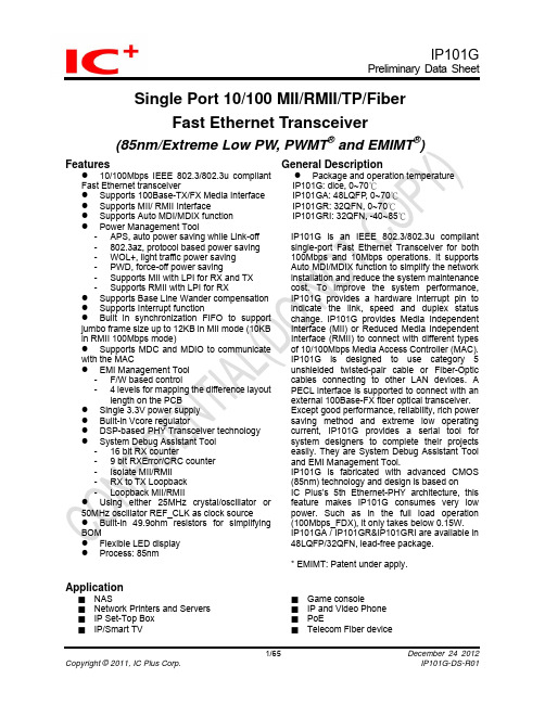
Single Port 10/100 MII/RMII/TP/FiberFast Ethernet Transceiver(85nm/Extreme Low PW, PWMT ® and EMIMT ®)Features General DescriptionIP1IP1IP1IP1z 10/100Mbps IEEE 802.3/802.3u compliant Fast Ethernet transceiverz Supports 100Base-TX/FX Media Interface z Supports MII/ RMII Interfacez Supports Auto MDI/MDIX function z Power Management Tool- APS, auto power saving while Link-off - 802.3az, protocol based power saving - WOL+, light traffic power saving - PWD, force-off power saving- Supports MII with LPI for RX and TX - Supports RMII with LPI for RXz Supports Base Line Wander compensation z Supports Interrupt functionz Built in synchronization FIFO to support jumbo frame size up to 12KB in MII mode (10KB in RMII 100Mbps mode)z Supports MDC and MDIO to communicate with the MACz EMI Management Tool - F/W based control- 4 levels for mapping the difference layoutlength on the PCBz Single 3.3V power supply z Built-in Vcore regulatorz DSP-based PHY Transceiver technology z System Debug Assistant Tool - 16 bit RX counter- 9 bit RXError/CRC counter - Isolate MII/RMII - RX to TX Loopback - Loopback MII/RMIIz Using either 25MHz crystal/oscillator or 50MHz oscillator REF_CLK as clock sourcez Built-in 49.9ohm resistors for simplifying BOMz Flexible LED display z Process: 85nmz Package and operation temperature 01G: dice, 0~70℃01GA: 48LQFP , 0~70℃ 01GR: 32QFN, 0~70℃ 01GRI: 32QFN, -40~85℃IP101G is an IEEE 802.3/802.3u compliant single-port Fast Ethernet Transceiver for both 100Mbps and 10Mbps operations. It supports Auto MDI/MDIX function to simplify the network installation and reduce the system maintenance cost. To improve the system performance, IP101G provides a hardware interrupt pin to indicate the link, speed and duplex status change. IP101G provides Media Independent Interface (MII) or Reduced Media Independent Interface (RMII) to connect with different types of 10/100Mbps Media Access Controller (MAC). IP101G is designed to use category 5 unshielded twisted-pair cable or Fiber-Optic cables connecting to other LAN devices. A PECL interface is supported to connect with an external 100Base-FX fiber optical transceiver. Except good performance, reliability, rich power saving method and extreme low operating current, IP101G provides a serial tool for system designers to complete their projects easily. They are System Debug Assistant Tool and EMI Management Tool.IP101G is fabricated with advanced CMOS (85nm) technology and design is based onIC Plus’s 5th Ethernet-PHY architecture, this feature makes IP101G consumes very low power. Such as in the full load operation (100Mbps_FDX), it only takes below 0.15W. IP101GA / IP101GR&IP101GRI are available in 48LQFP/32QFN, lead-free package.* EMIMT: Patent under apply.Application■ NAS■ Network Printers and Servers ■ IP Set-Top Box ■IP/Smart TV■ Game console■ IP and Video Phone ■ PoE■Telecom Fiber deviceTable Of ContentsTable Of Contents (2)List of Figures (4)List of Tables (5)Revision History (6)Features comparison between IP101G and IP101A/IP101AH (7)Transmit and Receive Data Path Block Diagram (8)1Pin diagram (9)2Dice pad information (11)3Pin description (12)3.1IP101GA pin description (12)3.2IP101GR/GRI pin description (16)4Register Descriptions (19)4.1Register Page mode Control Register (20)4.2MII Registers (20)4.3MMD Control Register (30)4.4MMD Data Register (31)4.5RX Counter Register (34)4.6LED Mode Control Register (35)4.7WOL+ Control Register (35)4.8UTP PHY Specific Control Register (38)4.9Digital IO Pin Control Register (39)5Function Description (41)5.1Major Functional Block Description (41)5.1.1Transmission Description (41)5.1.2MII and Management Control Interface (42)5.1.3RMII Interface (43)5.1.4Flexible Clock Source (45)5.1.5Auto-Negotiation and Related Information (45)5.1.6Auto-MDIX function (46)5.2PHY Address Configuration (46)5.3Power Management Tool (47)5.3.1Auto Power Saving Mode (47)5.3.2IEEE802.3az EEE (Energy Efficient Ethernet) (48)5.3.3Force power down (48)5.3.4WOL+ operation mode (48)5.4LED Mode Configuration (52)5.5LED Blink Timing (52)5.6Repeater Mode (52)5.7Interrupt (52)5.8Miscellaneous (52)5.9Serial Management Interface (53)5.10Fiber Mode Setting (54)5.11Jumbo Frame (54)6Layout Guideline (55)6.1General Layout Guideline (55)6.2Twisted Pair recommendation (55)7Electrical Characteristics (56)7.1Absolute Maximum Rating (56)7.2DC Characteristics (56)7.3Crystal Specifications (57)7.4AC Timing (58)7.4.1Reset, Pin Latched-in, Clock and Power Source (58)7.4.2MII Timing (59)7.4.3RMII Timing (60)7.4.4SMI Timing (61)7.5Thermal Data (61)8Order Information (62)9Physical Dimensions (63)9.148-PIN LQFP (63)9.232-PIN QFN (64)List of FiguresFigure 1 Flow chart of IP101G (8)Figure 2 IP101GA 48 Pin Diagram (9)Figure 3 IP101GR/GRI 32 Pin Diagram (10)Figure 4 IP101G dice pad information (11)Figure 5 LPI transition (43)Figure 6 IP101G/GA/GR/GRI MII Mode with LPI transition Block Diagram (43)Figure 7 IP101G/GA/GR/GRI MII Mode without LPI transition Block Diagram (43)Figure 8 IP101G RMII Mode with internal clock Block Diagram (44)Figure 9 IP101G RMII Mode with external clock Block Diagram (44)Figure 10 IP101G RMII Clock Application Circuit (45)Figure 11 IP101G link speed and EEE ability programming guide (46)Figure 12 PHY Address Configuration (47)Figure 13 Magic Packet Format (49)Figure 14 Sleep or wake up automatically programming guide (50)Figure 15 MAC control sleep or wake up programming guide (51)Figure 16 MDC/MDIO Format (53)Figure 17 IP101G Fiber Mode Setting (54)Figure 18 Reset, Pin Latched-In, Clock and Power Source Timing Requirements (58)Figure 19 MII Transmit Timing Requirements (59)Figure 20 MII Receive Timing Specifications (59)Figure 21 RMII Transmit Timing Requirements (60)Figure 22 RMII Receive Timing Specifications (60)Figure 23 SMI Timing Requirements (61)Figure 24 48-PIN LQFP Dimension (63)Figure 25 32-PIN QFN Dimension (64)List of TablesTable 1 Features comparison between IP101G and IP101A/IP101AH (7)Table 2 Register Map (19)Table 3 Flexible Clock Source Setting (45)Table 4 PHY Address Configuration (47)Table 5 WOL+ operation mode (49)Table 6 LED Mode 1 Function (52)Table 7 LED Mode 2 Function (52)Table 8 LED Blink Timing (52)Table 9 SMI Format (53)Table 10 DC Characteristics (56)Table 11 I/O Electrical Characteristics (56)Table 12 Pin Latched-in Configuration Resistor (57)Table 13 Crystal Specifications (57)Table 14 Reset, Pin Latched-in, Clock and Power Source Timing Requirements (58)Table 15 MII Transmit Timing Requirements (59)Table 16 MII Receive Timing Specifications (59)Table 17 RMII Transmit Timing Requirements (60)Table 18 RMII Receive Timing Specifications (60)Table 19 SMI Timing Requirements (61)Table 20 Thermal Data (61)Table 21 Part Number and Package (62)Revision HistoryRevision # Change DescriptionIP101G-DS-R01 Initial release.IP101G-DS-R01-20120522 1) Correct the typo of Digital IO Pin Control Register.2) Modify the operation voltage REGOUT and DVDD_REGIN of DCCharacteristics.IP101G-DS-R01-20120611 1) Correct the typo of Linear Regulator Output Control Register.2) Correct the typo of pin description for pin type PD and PU.3) Modify the register description for RMII_V12 and RMII_V10.4) Correct the typo of register default values.5) Modify the operation voltage DVDD33_IO of DC Characteristics.IP101G-DS-R01-20120622 Add 30 seconds into the definition for register WOL_PLUS_TIMER_SEL.IP101G-DS-R01-20120629 Add the symbol SC (Self Clear) for PHY MII register 0.15 Reset and 0.9Restart Auto-Negotiation.IP101G-DS-R01-20120709 1) Add LED mode 2 in the pin description and function description.2) Correct the table of LED Blink Timing.3) Add more description of PHY Address Configuration and IEEE 802.3az.4) Add ESD reliability of Absolute Maximum Rating.5) Correct the typo of function description for Auto Power Saving Mode.6) Change register P16R16[10] description from HEART_BEAT_EN toReserved.IP101G-DS-R01-20120719 Correct the table of Register Map for page selection.IP101G-DS-R01-20120726 1) Add more description of Register RX2TX_LPBK P1R23[13] for Rx to Txloopback test.2) Add more description on Fiber Mode Setting and latched-in pin signalson AC Timing.3) Add IP101AH into the table of features comparison.IP101G-DS-R01-20120808 1) Correct the I/O type of IP101GA pin description to O(Ouput) for pin24RXER.2) Change the pin name from DVDD33_IO to VDDIO.IP101G-DS-R01-20120821 1) Change the default value of register P16R27 from 0x0022 to 0x0012.2) Remove I/O Slew Rate Control Register.3) Change the register location RMII_WITH_ER from P16R29[0] toP16R29[7].IP101G-DS-R01-20120927 1) Add more description of low power idle (LPI) state in MII and RMIImodes.2) Correct the typo of Physical Dimensions.IP101G-DS-R01-20121101 Change the LED blink timing from “On 80ms -> Off (20~40)ms” to “On 26ms-> Off 78ms”.IP101G-DS-R01-20121113 Add more function description to support Jumbo Frame.IP101G-DS-R01-20121127 Change the LED mode function as same as IP101A.IP101G-DS-R01-20121224 Add the notice that does not let these PHY address pins floating for thelatched-in settings after the power is ready.DisclaimerThis document probably contains the inaccurate data or typographic error. In order to keep this document correct, IC Plus reserves the right to change or improve the content of this document.Features comparison between IP101G and IP101A/IP101AHTable 1 Features comparison between IP101G and IP101A/IP101AHProduct Name IP101GR IP101G IP101GA IP101A IP101AH Package Type 32pin QFN Dice 48pin LQFP48pin LQFPREGOUT(1) Output Voltage and location 1.0V, pin28 1.0V, pad5and pad111.0V, pin82.5V, pin32REGIN Input Voltage and location NA(2) 1.0V, pad23and pad26NA 2.5V, pin8RMII mode setting Pin4 Pad18 Pin1 Pin1 and pin44Fiber mode setting: Fiber FXSD signal: Pin19Pin1Pad39Pad13Pin22Pin43NA Pin24 and pin48Pin37Number of LED 2 4 4 5LED mode 1 and 2 1 and 2LED Blink Timing On 26ms -> Off 78ms On 26ms -> Off 78msPHY address number(3) Single: 0 ~ 1Multi: 2 ~ 31Single: 0 ~ 7Multi: 8 ~ 31Single: 0 ~ 31Center-tap of transformer Do not connect to any power 2.5V input power Built-in 49.9ohm resistors Yes No Power consumption ~150mW ~480mW Process 85nm 0.25μm IEEE 802.3az Yes No10Base TX amplitude ~1.75V (10Base-Te) ~2.5V (10Base-T) WOL+ (Wake On LAN Plus) Yes NoAnalog OFF Yes No16 bit RX counter Yes No9 bit RXER/CRC counter Yes NoRX to TX Loopback Yes No Loopback MII/RMII Yes YesSNI mode No Yes Note 1: Regulator voltage output is for internal use only. Do not supply to any other device.Note 2: Not available for this function. The 1.0V is supplied by the regulator that built-in the chip.Note 3: Do not let these PHY address pins floating for the latched-in settings after the power is ready.Transmit and Receive Data Path Block DiagramFigure 1 Flow chart of IP101G1Pin diagramRXER CRS/LEDMODRXDV/CRS_DV/FX_HEN X1X2RXD2RXD3RXCLK/50M_CLKO DGNDRXD0NCRESET_N IP101GA (LQFP-48)242322212019181716NC NC TXER/FXSDNC Note:Those pins in "blue "are different from IP101A.NC RXD1INTRNC DGNDNC LED3/PHY_AD3VDDIOFigure 2 IP101GA 48 Pin DiagramIP101GR/GRI(VQFN-32)(GND on bottom of chip)RXD3TXCLK/50M_CLKI RXCLK/50M_CLKO LED0/PHY_AD0LED3/PHY_AD3161514131211109RESET_NISET REGOUT MDI_TN MDI_TP MDI_RP MDI_RN RXD2AVDD33Figure 3 IP101GR/GRI 32 Pin Diagram2Dice pad informationIC LogoPad 1Pad 44Pad 11Pad 45Pad 24Pad 31Pad 12Pad 22Pad 23REGINPHYAD_LED028PHYAD_LED129VSS30PHYAD_LED231PHYAD_LED332VDDIO 33RX_CLK REGOUT 34VSSIO RESET_N 35RXD[3]TXER_FXSD 36RXD[2]VSSIO 37RXD[1]15X138RXD[0]16X239RXDV_FIBMOD 17INTR40CRS18COL_RMII 41RXER_INTR 19TX_EN 4220TXD[3]21TXD[2]22TXD[1]23REGINFigure 4 IP101G dice pad information3 Pin descriptionType Description Type DescriptionLI Latched Input in power up or reset PD Internal Pull-Down 250KΩI/O Bi-directional input and output PU Internal Pull-Up 250KΩI Input Hi-Z High impedanceO Output P PowerOD Open Drain3.1 IP101GA pin descriptionIP101GAPin no. Label Type ResetStateDescriptionSerial Management Interface Pins25 MDC I Hi-Z Management Data Interface Clock: This pin provides aclock reference to MDIO. The clock rate can be up to2.5MHz.26 MDIO I/O(PU)I(PU)Management Data interface Input/Output:Thefunction of this pin is to transfer management informationbetween PHY and MAC.MII/RMII Pins2 TXEN I(PD)I(PD)Transmit Enable or Signal Detect.43 TXER/FXSD I(PD)I(PD)Transmit Error or FXSD:This is a dual-function pin which is determined by themedia type selection. If RXDV/CRS_DV/FX_HEN islatched as “0 (default)” upon reset, the TP interface isselected and its function as TXER. If the fiber interface isselected, this pin’s function as FXSD.FXSD:0: Fiber link down; 1: Fiber link upTransmit Enable:TXEN TXER Description1 1 Transmission errorpropagation.0 1 Combine TXD[3:0] that equalto 0001 for request PHY toenter LPI mode.1 00 0Normal operationThis pin TXER must be either floating or connecting toGND in RMII mode.7 TXCLK/50M_CLKI I/O Hi-Z Transmit Clock output or 50M clock input:In MII mode,this pin provides a continuous 25MHz clockat 100Base-TX and 2.5MHz at 10Base-T.In RMII mode, a 50Mhz clock should input to this pin forthe timing reference of the internal circuit.3,4,5,6 TXD[3:0] I Hi-Z Transmit Data Input:IP101GAPin no.LabelType ResetDescriptionStateIn MII mode, TXD[3:0] is synchronous to TXCLK.In RMII mode, TXD[1:0] is synchronous to 50M_CLKI.22 RXDV/CRS_DV/ FX_HEN O/LI (PD) I (PD)Receive Data Valid or Media Type Selection:FX_HENThe input state is latched upon reset to determine whether TP or fiber interface is selected. If it is at logic “0” (default) state upon reset, the TP interface is selected; otherwise the fiber interface is selected. RXDV/CRS_DVIn MII mode, this pin indicates the Receive Data Valid function.In RMII mode, this pin indicates the Carrier Sense and Receive Data Valid function.16 RXCLK/ 50M_CLKO O Hi-Z Receive Clock:In MII mode, this pin provides 25MHz for 100BT or2.5MHz for 10BT.In RMII mode, this pin output a 50 MHz clock for the timing reference of MAC side.18,19, 20,21 RXD[3:0] O Hi-Z Receive Data: In MII mode, RXD[3:0] is synchronous to RXCLK.In RMII mode, RXD[1:0] is synchronous to 50M_CLKI.24 RXER O Hi-Z Receive error:RXDV RXER Description1 1 Decoding error of thereceived signal0 1 Combine RXD[3:0] equal to0001 indicates PHY isreceiving LPI.1 0Normal operation This pin RXER is an optional input for MAC/CPU device.1 COL/RMII O/LI (PD) I (PD)Collision Detected:During the normal operation, thispin outputs a high status signal it means collision isdetected.RMII Mode Selection: During the power on reset, thispin status is latched to determine what kind MAC interface will be used. Logic “1” is for RMII mode and logic “0” is for MII mode.23 CRS/LEDMOD O/LI (PD) I (PD)Carrier Sense: When signal output from this pin is highindicates the transmission or reception is in process andat low status means the line is in idle state.LEDMOD: During power on reset, this pin status is latched to determine which either LED mode 1 or 2is selected, please refer to the LED pins description.Cable Transmission Interface 34,33 MDI_TP MDI_TN I/O I/O Hi-Z Transmit Output Pair: Differential pair shared by100Base-TX and 10Base-T modes. When configured as100Base-TX, output is an MLT-3 encoded waveform. When configured as 10Base-T , the output is ManchesterIP101GAPin no. Label Type Reset DescriptionStatecode.31,30 MDI_RPMDI_RN I/OI/OHi-Z Receive Input Pair: Differential pair shared by 100Base-TX and 10Base-T modes.Clock and Miscellaneous Pins47 X2 O O25MHz Crystal Output: Connects to crystal to providethe 25MHz output. It must be left open when X1 is drivenwith an external 25MHz oscillator.46 X1 I I 25MHz Crystal Input: Connects to crystal to provide the25MHz crystal input. If a 25MHz oscillator is used,connect X1 to the oscillator’s output. If a 50MHz clock isapplied to pin7 TXCLK/50M_CLKI, X1 must beconnected to GND or AGND33.42 RESET_N I I(PU)RESET_N: Enable a low status signal will reset the chip. For a complete reset function. 25MHz clock (x1) must be active for a minimum of 10 clock cycles before the rising edge of RESET_N. Chip will be able to operate after 2.5ms delay of the rising edge of RESET_N. The 2.5ms extension is to ensure the stability of system power.28 ISET I I Bandgap Circuit Resistor: This pin should beconnected to GND via a 6.19KΩ (1%) resistor to definethe standard current of the internal circuit.48 INTR OD Hi-Z Interrupt: Programmable Interrupt Output, this is anopen drain output, and an external pulled-up resistor isneeded for normal mode operation. Another operationmode is Rx to Tx loopback debugging test (reflect onRegister P1R23[13] RX2TX_LPBK) when connect INTRpin to GND.9 LED0/PHY_AD0 O/LI Hi-Z LED 0 and PHY Address [0]LED 0LED mode1 2LED0Link Link /ACT(blinking)10 LED1/PHY_AD1 O/LI Hi-Z LED 1 and PHY Address [1]LED1LED mode1 2LED1Duplex Duplex /COL (blinking)12 LED2/PHY_AD2 O/LI Hi-Z LED 2 and PHY Address [2]LED2LED mode1 2LED210M Link /ACT10M Link13 LED3/PHY_AD3 O/LI(PD) Hi-Z LED 3 and PHY Address [3]LED3LED mode1 2LED3100M Link /ACT 100M Link27 TEST_ON I I Test Enable: Set this pin to high to enable Test mode.IP101GAPin no. Label Type Reset DescriptionState(PD) (PD)For normal operation, this pin doesn’t need to beconnected.Power and Ground32 NC -- -- It’s a NC pin.8 REGOUT P P Regulator Power Output: This is a regulator poweroutput. A 10uF and 0.1uF should be connected to this pinto filter the power noise.14 VDDIO P P Digital Power input:Either 3.3V or 2.5V for I/O power supply.36 AVDD33 P P 3.3V Analog power input: This is a 3.3V power supplyfor analog circuitry, and it should be decoupled carefully.35 AGND33 P P Ground.29 AGND1V P P Ground45,11,17 DGND P P Ground.3.2 IP101GR/GRI pin descriptionIP101GR/GRIPin no. Label Type ResetStateDescriptionSerial Management Interface Pins22 MDC I Hi-Z Management Data Interface Clock: This pin provides aclock reference to MDIO. The clock rate can be up to2.5MHz.23 MDIO I/O(PU)I(PU)Management Data interface Input/Output:Thefunction of this pin is to transfer management informationbetween PHY and MAC.MII/RMII Pins5 TXEN I(PD)I(PD)Transmit Enable or Signal Detect.1 TXER/FXSD I(PD)I(PD)Transmit Error or FXSD:This is a dual-function pin which is determined by themedia type selection. If RXDV/CRS_DV/FX_HEN islatched as “0 (default)” upon reset, the TP interface isselected and its function as TXER. If the fiber interface isselected, this pin’s function as FXSD.FXSD:0: Fiber link down; 1: Fiber link upTransmit Enable:TXEN TXER Description1 1 Transmission errorpropagation.0 1 Combine TXD[3:0] that equalto 0001 for request PHY toenter LPI mode.1 00 0Normal operationThis pin TXER must be either floating or connecting toGND in RMII mode.10 TXCLK/50M_CLKI I/O Hi-Z Transmit Clock output or 50M clock input:In MII mode,this pin provides a continuous 25MHz clockat 100Base-TX and 2.5MHz at 10Base-T.In RMII mode, a 50Mhz clock should input to this pin forthe timing reference of the internal circuit.6,7,8,9 TXD[3:0] I Hi-Z Transmit Data Input:In MII mode, TXD[3:0] is synchronous to TXCLK.In RMII mode, TXD[1:0] is synchronous to 50M_CLKI.19 RXDV/CRS_DV/FX_HEN O/LI(PD)I(PD)Receive Data Valid or Media Type Selection:FX_HENThe input state is latched upon reset to determinewhether TP or fiber interface is selected. If it is at logic“0” (default) state upon reset, the TP interface isselected; otherwise the fiber interface is selected.RXDV/CRS_DVIn MII mode, this pin indicates the Receive Data ValidIP101GR/GRIPin no.LabelType ResetDescriptionStatefunction.In RMII mode,this pin indicates the Carrier Sense and Receive Data Valid function.14 RXCLK/ 50M_CLKO O Hi-Z Receive Clock:In MII mode, this pin provides 25MHz for 100BT or2.5MHz for 10BT.In RMII mode, this pin output a 50 MHz clock for the timing reference of MAC side.15,16, 17,18 RXD[3:0] O Hi-Z Receive Data: In MII mode, RXD[3:0] is synchronous to RXCLK.In RMII mode, RXD[1:0] is synchronous to 50M_CLKI.21 RXER/INTR_32 O/ODHi-Z The multiplex function of this pin is set by the registerSEL_INTR32, page 16, 29[2]. The default function is RXER.Receive error:RXDV RXER Description 1 1 Decoding error of thereceived signal0 1 Combine RXD[3:0] equal to0001 indicates PHY is receiving LPI. 1 0Normal operationThis pin RXER is an optional input for MAC/CPU device.Interrupt: Programmable Interrupt Output, this is an open drain output, and an external pulled-up resistor is needed.4 COL/RMII O/LI (PD) I (PD)Collision Detected:During the normal operation, thispin outputs a high status signal it means collision isdetected.RMII Mode Selection: During the power on reset, thispin status is latched to determine what kind MAC interface will be used. Logic “1” is for RMII mode and logic “0” is for MII mode.20 CRS/LEDMOD O/LI (PD) I (PD)Carrier Sense:When signal output from this pin is highindicates the transmission or reception is in process andat low status means the line is in idle state.LEDMOD: During power on reset, this pin status is latched to determine which either LED mode 1 or 2is selected, please refer to the LED pins description.Cable Transmission Interface 30,29 MDI_TP MDI_TN I/O I/O Hi-Z Transmit Output Pair: Differential pair shared by100Base-TX and 10Base-T modes. When configured as100Base-TX, output is an MLT-3 encoded waveform. When configured as 10Base-T , the output is Manchester code.27,26 MDI_RP MDI_RN I/O I/O Hi-Z Receive Input Pair: Differential pair shared by100Base-TX and 10Base-T modes.Clock and Miscellaneous PinsIP101GR/GRIPin no. Label Type Reset DescriptionState3 X2 O O25MHz Crystal Output: Connects to crystal to providethe 25MHz output. It must be left open when X1 is drivenwith an external 25MHz oscillator.2 X1 I I 25MHz Crystal Input: Connects to crystal to provide the25MHz crystal input. If a 25MHz oscillator is used,connect X1 to the oscillator’s output. If a 50MHz clock isapplied to pin10 TXCLK/50M_CLKI, X1 must beconnected to GND.32 RESET_N I I(PU)RESET_N: Enable a low status signal will reset the chip. For a complete reset function. 25MHz clock (x1) must be active for a minimum of 10 clock cycles before the rising edge of RESET_N. Chip will be able to operate after 2.5ms delay of the rising edge of RESET_N. The 2.5ms extension is to ensure the stability of system power.25 ISET I I Bandgap Circuit Resistor: This pin should beconnected to GND via a 6.19KΩ (1%) resistor to definethe standard current of the internal circuit.11 LED0/PHY_AD0 O/LI Hi-Z LED 0 and PHY Address [0]LED 0LED mode1 2LED0Link Link /ACT(blinking)12 LED3/PHY_AD3 O/LI(PD) Hi-Z LED 3 and PHY Address [3]LED3LED mode1 2LED3100M Link /ACT 100M Link24 TEST_ON I(PD)I(PD)Test Enable: Set this pin to high to enable Test mode.For normal operation, this pin doesn’t need to beconnected.Power and Ground28 REGOUT P P Regulator Power Output: This is a regulator poweroutput. A 10uF and 0.1uF should be connected to this pinto filter the power noise.13 VDDIO P P Digital Power input:IP101GR: Either 3.3V or 2.5V for I/O power supply.IP101GRI: 3.3V for I/O power supply.31 AVDD33 P P 3.3V Analog power input: This is a 3.3V power supplyfor analog circuitry, and it should be decoupled carefully. BottomPADGND P P Ground.4 Register DescriptionsTable 2 Register MapPage Register Description Default NoteX 20 Page Control Register 0x0010-- 0 Control Register 0x3100-- 1 Status Register 0x7849-- 2 PHY Identifier 1 Register 0x0243-- 3 PHY Identifier 2 Register 0x0C54-- 4 Auto-Negotiation Advertisement Register 0x01E1-- 5 Auto-Negotiation Link Partner Ability Register 0x0000-- 6 Auto-Negotiation Expansion Register 0x0004-- 7 Auto-Negotiation Next Page Transmit Register 0x2001-- 8 Auto-Negotiation Link Partner Next Page Register 0x0000-- 13 MMD Access Control Register 0x0000-- 14 MMD Access Address Data Register 0x000016 16 PHY Specific Control Register 0x000216 17 PHY Interrupt Ctrl/Status Register 0x0F0016 18 PHY Status Monitoring Register 0x020816 26 Digital IO Pin Driving Control Register 0x124916 27 Digital IO Pin Driving Control Register 0x001216 29 Digital I/O Specific Control Register 0x008216 30 PHY MDI/MDIX Control and Specific Status Register 0x0000-- MMD 3.0 PCS Control 1 Register 0x0000-- MMD 3.1 PCS Status 1 Register 0x0000-- MMD 3.20 EEE Capability Register 0x0002-- MMD 3.22 EEE Wake Error Count Register 0x0000-- MMD 7.60 EEE Advertisement Register 0x0002-- MMD 7.61 EEE Link Partner Ability Register 0x00001 17 PHY Specific Control Register 0x00001 18 RX CRC Error Counter Register 0x00001 22 Linear Regulator Output Control Register 0x20201 23 UTP PHY Specific Control Register 0x80002 18 RX Packet Counter Register 0x00003 16 LED Control Register 0x00004 16 WOL+ Control Register 0x5F404 22 Digital IO Pin Driving Control Register 0x40005 16 PHY WOL+ MAC Address Register 0x00008 17 RX Counter Control Register 0x700011 18 UTP PHY Interrupt Control/Status Register 0x0000Page Register DescriptionDefault Note 17 17 PHY WOL+ Status Register0x0000 1817RX Counter Interrupt Control/Status Register0x0000Register descriptionsR/W = Read/Write, SC = Self-Clearing, RO = Read Only, LL = Latching Low, LH = Latching High (TP): for twisted pair operation. (FX): for fiber operation. (e-fuse): only available for IP101G (dice).4.1 Register Page mode Control RegisterMII register 20 PHYMIIROMR/WDescriptionDefaultPage Control Register -- 20[4:0] -- R/W Reg16~31_Page_Sel[4:0] Register Page Select0x10The other Registers are reserved registers. User is inhibited to access to these registers. It may introduce abnormal function to write these registers.4.2 MII RegistersBitNameDescription/UsageDefault value (h): 3100Register 0 : Control Register 15 ResetWhen set, this action will bring both status and control registers of the PHY to default state. This bit is self-clearing. 1 = Software reset 0 = Normal operation0, RW/SC 14 LoopbackThis bit enables loopback of transmit data to the receive data path, i.e., TXD to RXD. 1 = enable loopback 0 = normal operation0, RW 13 Speed SelectionThis bit sets the speed of transmission. 1 = 100Mbps 0 = 10MbpsAfter completing auto-negotiation, this bit will reflect the speed status.(1: 100Mbps, 0: 10Mbps)1, RW 12 Auto-Negotiation Enable This bit determines the auto-negotiation function. 1 = enable auto-negotiation; bits 13 and 8 will be ignored. 0 = disable auto-negotiation; bits 13 and 8 will determine the link speed and the data transfer mode, under this condition.1, RW (TP) 0, RO (FX) 11 Power DownThis bit will turn down the power of the PHY chip and the internal crystal oscillator circuit if this bit is enabled. The MDC and MDIO are still activated for accessing to the MAC. 1 = power down0 = normal operation0, RW 10 Isolate1=electrically Isolate PHY from MII but not isolate MDC and MDIO0,RW。
Richtek RT9069 低电压线性调压器说明书

RT9069Copyright © 2018 Richtek Technology Corporation. All rights reserved. is a registered trademark of Richtek Technology Corporation.DS9069-09 November 201836V, 2μA I Q , Peak 200mA Low Dropout Voltage Linear RegulatorGeneral DescriptionThe RT9069 is a low-dropout (LDO) voltage regulators with enable function offering the benefits of high input voltage, low-dropout voltage, low-power consumption, and miniaturized packaging.The features of low quiescent current as low as 2μA and zero disable current is ideal for powering the battery equipment to a longer service life. The RT9069 is stable with the ceramic output capacitor over its wide input range from 3.5V to 36V and the entire range of output load current.Applications● Portable, Battery Powered Equipments ● Extra Low Voltage Microcontrollers ●Notebook ComputersMarking InformationFor marking information, contact our sales representative directly or through a Richtek distributor located in your area. Note :Richtek products are :④ RoHScompliant and compatible with the currentrequirements of IPC/JEDEC J-STD-020.④ Suitable for use in SnPb or Pb-free soldering processes.Simplified Application CircuitFeatures● 2μA Ground Current at no Load ● ±2% Output Accuracy● 100mA Continuous Output Current ● Zero Disable Current● Maximum Operating Input Voltage 36V ● Dropout Voltage: 0.2V at 10mA/ VIN 5V●Support Fixed Output Voltage 2.5V, 3V, 3.3V, 5V, 9V, 12V● Stable with Ceramic or Tantalum Capacitor ● Current Limit Protection● Over-Temperature Protection●RoHS Compliant and Halogen FreeOrdering InformationRT9069- 25 : 2.5V 30 : 3V 33 : 3.3V 50 : 5V90: 9V C0: 12VSpecial Request: Any Voltage between 2.5V and 12V under specific business agreementV OUTVRT9069Pin Configuration(TOP VIEW)VCC NC VOUT NCEN GND NCNCVCC NC GND NC ENVOUT541236G N D7SOP-8 (Exposed Pad) SOT-23-5SOT-89-5UDFN-6L 1.6x1.6Functional Pin DescriptionRT9069Functional Block DiagramVCCGNDENVOUT OperationBasic OperationThe RT9069 is a high input voltage linear regulator designed especially for low external component systems. The input voltage range is from 3.5V to 36V. The minimum required output capacitance for stable operation is 1μF effective capacitance after consideration of the temperature and voltage coefficient of the capacitor.Output TransistorThe RT9069 builds in a P-MOSFET output transistor which provides a low switch-on resistance for low dropout voltage applications.Error AmplifierThe Error Amplifier compares the internal reference voltage with the output feedback voltage from the internal divider, and controls the Gate voltage of P-MOSFET to support good line regulation and load regulation at output voltage. EnableThe RT9069 delivers the output power when it is set to enable state. When it works in disable state, there is no output power and the operation quiescent current is zero.Current Limit ProtectionThe RT9069 provides current limit function to prevent the device from damages during over-load or shorted-circuit conditions. This current is detected by an internal sensing transistor.Over-Temperature ProtectionThe over-temperature protection function turns off the P-MOSFET when the junction temperature exceeds 150︒C (typ.) and the output current exceeds 4mA. Once the junction temperature cools down by approximately 20︒C, the regulator automatically resumes operation.RT9069Absolute Maximum Ratings (Note 1)●VCC, EN to GND ---------------------------------------------------------------------------------------------------- -0.3V to 40V●VOUT to VCC -------------------------------------------------------------------------------------------------------- -40V to 0.3V●VOUT to GNDRT9069-90/RT9069-C0 ------------------------------------------------------------------------------------------- -0.3V to 15V RT9069-25/RT9069-30/RT9069-33/RT9069-50 ------------------------------------------------------------ -0.3V to 6V●Power Dissipation, P D @ T A= 25°CSOP-8 (Exposed Pad) ---------------------------------------------------------------------------------------------- 3.26WSOT-23-5 ------------------------------------------------------------------------------------------------------------- 0.45WSOT-89-5 ------------------------------------------------------------------------------------------------------------- 0.87WUDFN-6L 1.6x1.6 --------------------------------------------------------------------------------------------------- 2.15W●Package Thermal Resistance (Note 2)SOP-8 (Exposed Pad), θJA--------------------------------------------------------------------------------------- 30.6°C/W SOP-8 (Exposed Pad), θJC--------------------------------------------------------------------------------------- 3.4°C/W SOT-23-5, θJA-------------------------------------------------------------------------------------------------------- 218.1°C/W SOT-23-5, θJC-------------------------------------------------------------------------------------------------------- 28.5°C/W SOT-89-5, θJA -------------------------------------------------------------------------------------------------------- 113.9°C/W SOT-89-5, θJC ------------------------------------------------------------------------------------------------------- 6.9°C/W UDFN-6L 1.6x1.6, θJA --------------------------------------------------------------------------------------------- 46.5°C/W UDFN-6L 1.6x1.6, θJC --------------------------------------------------------------------------------------------- 18.6°C/W●Lead Temperature (Soldering, 10 sec.) -------------------------------------------------------------------------260︒C●Junction Temperature -----------------------------------------------------------------------------------------------150︒C●Storage Temperature Range --------------------------------------------------------------------------------------- -65︒C to 150︒C ●ESD Susceptibility (Note 3)HBM (Human Body Model) ---------------------------------------------------------------------------------------- 2kV Recommended Operating Conditions (Note 4)●Supply Input Voltage --------------------------------------------------------------------------------------------------3.5V to 36V●Junction Temperature Range --------------------------------------------------------------------------------------- -40︒C to 125︒C ●Ambient Temperature Range---------------------------------------------------------------------------------------- -40︒C to 85︒C Electrical Characteristics(C = 1μF, T= 25︒C, for each LDO unless otherwise specified)RT9069Note 1. Stresses beyond those listed under “Absolute Maximum Ratings” may cause permanent damage to the device. These are stress ratings only, and functional operation of the device at these or any other conditions beyond those indicated in the operational sections of the specifications is not implied. Exposure to absolute maximum rating conditions may affect device reliability.Note 2. θJA is measured at T A= 25︒C on a high effective thermal conductivity four-layer test board per JEDEC 51-7. θJC is measured at the exposed pad of the package.Note 3. Devices are ESD sensitive. Handling precaution is recommended.Note 4. The device is not guaranteed to function outside its operating conditions.RT9069Typical Application CircuitV OUTV CC3.5V to 36VμF)Note (1) : All the input and output capacitors are the suggested values, referring to the effective capacitances,subject to any de-rating effect, like a DC bias.RT9069Typical Operating Characteristics2.402.422.442.462.482.502.522.542.562.582.60-50-25255075100125O u t p u t V o l t a g e (V )Temperature (℃)Output Voltage vs. Temperature2.422.442.462.482.52.5250100150O u t p u t V o l t a g e (V )Output Current (mA)Output Voltage vs. Output Current2.42.452.52.552.6369121518212427303336O u t p u t V o l t a ge (V )Supply Voltage (V)Output Voltage vs. Supply Voltage1.51.61.71.81.92369121518212427303336Q u i e s c e n t C ur r e n t (μA )Supply Voltage (V)Quiescent Current vs. Supply Voltage0123456-50-25255075100125Q u i e s c e n t C u r r e n t (μA )Temperature(℃)Quiescent Current vs. Temperature020406080100369121518212427303336S H D N L e a k a g e C ur r e n t (n A )Supply Voltage (V)SHDN Input Leakage Current vs. V CCRT906900.20.40.60.811.21.41.6-50-25255075100125S H D N L e a k a g e C u r r e n t ( A )Temperature (℃)SHDN Leakage Input Current vs. Temp.00.511.52369121518212427303336E N V o l t a g e (V )Supply Voltage (V)Enable Threshold vs. Supply Voltage00.511.52-50-25255075100125E N V o l t a g e (V )Temperature (℃)Enable Threshold vs. Temperature00.10.20.30.40.5-50-25255075100125D r o p o u t V o l t a g e (V )Temperature (℃)Dropout Voltage vs. Temperature050100150200250300350-50-25255075100125C u r r e n t L i m i t (m A )Temperature (°C )Current Limit vs. TemperaturePSRR vs. Frequency-100-80-60-40-20101001000100001000001000000Frequency (Hz )P S R R (d B )RT9069Ground Current vs. Load Current501001502002503003500.0010.010.11101001000Load Curremt (mA)G N D C u r r e n t (u A)Dropout Voltage vs. Output Current0.00.51.01.52.02.53.03.54.04.55.0020406080100Output Current (mA)D r o p o u t V o l t a g e (V )Load Transient Response Time (250μs/Div)V OUT_ac (50mV/Div)I Load(50mA/Div)V CC = 12V, V OUT = 2.5V, I load = 10mA to 100mALoad Transient ResponseTime (250μs/Div)V OUT_ac (50mV/Div)I Load(50mA/Div)V CC = 24V, V OUT = 2.5V, I load = 10mA to 100mALoad Transient Response Time (250μs/Div)V OUT_ac(100mV/Div)I Load(100mA/Div)V CC = 12V, V OUT = 2.5V, I Load = 10mA to 200mALoad Transient ResponseTime (10μs/Div)V OUT_ac(100mV/Div)I Load(50mA/Div)V CC = 12V, V OUT = 2.5V, I Load = 10mA to 100mART9069Line Transient ResponseTime (100μs/Div)V OUT_ac (20mV/Div)VCC (5V/Div)V CC = 4.4V to 15V, V OUT = 2.5V, Load = 100mALine Transient ResponseTime (100μs/Div)V OUT_ac (20mV/Div)VCC (10V/Div)V CC = 3.5V to 36V, V OUT = 2.5V, Load = 100mAPower On from EN Time (25μs/Div)VCC (10V/Div)EN (2V/Div)V OUT (1V/Div)I Load(50mA/Div)V CC = 24V, V OUT = 2.5V, Load = 100mAPower Off from ENTime (25μs/Div)VCC (10V/Div)EN (2V/Div)V OUT (1V/Div)I Load(50mA/Div)V CC = 24V, V OUT = 2.5V, Load = 100mAApplication InformationThermal ConsiderationsFor continuous operation, do not exceed absolute maximum junction temperature. The maximum power dissipation depends on the thermal resistance of the IC package, PCB layout, rate of surrounding airflow, and difference between junction and ambient temperature. The maximum power dissipation can be calculated by the following formula :P D(MAX) = (T J(MAX) - T A) / θJAwhere TJ(MAX)is the maximum junction temperature, T A is the ambient temperature, and θJA is the junction to ambient thermal resistance.For recommended operating condition specifications, the maximum junction temperature is 125︒C. The junction to ambient thermal resistance, θJA, is layout dependent. For SOP-8 (Exposed Pad) packages, the thermal resistance, θJA, is 30.6︒C/W on a standard JEDEC 51-7 four-layer thermal test board. For SOT-23-5 package, the thermal resistance, θJA, is 218.1︒C/W on a standard JEDEC 51-7 four-layer thermal test board. For SOT-89-5 package, the thermal resistance, θJA, is 113.9︒C/W on a standard JEDEC 51-7 four-layer thermal test board. For UDFN-6L 1.6x1.6 package, the thermal resistance, θJA, is 46.5︒C/W on a standard JEDEC 51-7 four-layer thermal test board. The maximum power dissipation at T A= 25︒C can be calculated by the following formula : P D(MAX) = (125︒C - 25︒C) / (30.6︒C/W) = 3.2679W for SOT-8 (Exposed Pad) packageP D(MAX) = (125︒C - 25︒C) / (218.1︒C/W) = 0.4585W for SOT-23-5 packageP D(MAX) = (125︒C - 25︒C) / (113.9︒C/W) = 0.8779W for SOT-89-5 packageP D(MAX)= (125︒C -25︒C) / (46.5︒C/W) = 2.15W for UDFN-6L 1.6x1.6 package The maximum power dissipation depends on the operating ambient temperature for fixed T J(MAX)and thermal resistance, θJA. The derating curve in Figure 1 allows the designer to see the effect of rising ambient temperature on the maximum power dissipationFigure 1. Derating Curve of Maximum PowerDissipation0.00.51.01.52.02.53.03.54.00255075100125Ambient Temperature (°C)MaximumPowerDissipation(W)Outline Dimension8-Lead SOP (Exposed Pad) Plastic PackageBFHMI(Bottom of Package)SOT-23-5 Surface Mount Package5-Lead SOT-89 Surface Mount PackageU-Type 6L DFN 1.6x1.6 PackageRichtek Technology Corporation14F, No. 8, Tai Yuen 1st Street, Chupei CityHsinchu, Taiwan, R.O.C.Tel: (8863)5526789Richtek products are sold by description only. Customers should obtain the latest relevant information and data sheets before placing orders and should verify that such information is current and complete. Richtek cannot assume responsibility for use of any circuitry other than circuitry entirely embodied in a Richtek product. Information furnished by Richtek is believed to be accurate and reliable. However, no responsibility is assumed by Richtek or its subsidiaries for its use; nor for any infringements of patents or other rights of third parties which may result from its use. No license is granted by implication or otherwise under any patent or patent rights of Richtek or its subsidiaries.。
日立SU5000场发射扫描电子显微镜说明书

Fig. 1 External appearance of SU5000 FE-SEM New Schottky FE-SEM, SU5000Shigeaki Tachibana *1 William Podrazky *2Introduction1. Scanning Electron Microscopes (SEM) are used for observation and analysis in various fields. Since Field Emission SEM (FE-SEM) equipped with a field emission electron gun source provide higher resolution than those equipped with a thermionic emission electron gun source, the user base for FE-SEM has broadened significantly due to the need to observe specimen features continually decreasing in size. FE-SEMs are increasingly recognized as a tool for performing various surface analyses, however detection technologies for various signals generated from specimens have advanced beyond topographic observation alone. Typically the operator must utilize previous knowledge, training, and skill in microscopy to generate desirable results; therefore, optimal performance may vary based on experience level. For example, optimal performance may not be realized as a result of improper optical axis alignment or astigmatism correction, utilizing unsuitable accelerating voltage(s), or other parameters. Integrating an automated solution for these problems would allow the user to focus on obtaining comprehensive results under the best possible conditions at all times. Hitachi High-Technologies has developed a novel user interface which augments conventional SEM techniques to assist these problems. The “EM Wizard” user interface was developed to bring “new usability” to EM operators of various levels of experience. This Schottky FE-SEM, the SU5000, incorporated with EM Wizard interface, launched in August 2014 (Fig. 1).Fig. 2 EM Wizard, objectives selection screen.New Interface: EM Wizard2. With EM Wizard, rather than setting individual conditions such as the accelerating voltage, working distance, detector, and other parameters, the operator can select an “Observation Purpose,” such as “Surface Information” or “Elemental Information,” from a selection menu (*2). On the screen, a Radar Chart displays the type of content that will be acquired (resolution, surface information, elemental composition), and a simulated SEM image representing how a specimen will appear under each observational objective. This information provides a visual understanding of SEM image characteristics that can guide the operator in selecting these objectives (Fig. 2). When an “Observation Purpose” is selected, related system parameters are set automatically (e.g., accelerating voltage, working distance, detector), and optical axis parameters as well as astigmatism corrections are adjusted to optimal values. Simply by adjusting the brightness/contrast and focus, the operator can easily acquire high quality images at consistent resolution. In addition to an applications selection menu, what makes these functions possible are high-precision automation technologies initially developed for Critical Dimension (CD) SEM. CD-SEM are entirely automated, and must provide highly reproducible measurements, optical axis alignments, and other adjustments; EM Wizard has been designed to use these automation technologies to reproduce and maintain highly precise adjustments invariably. Because optical axis alignment and astigmatism correction values change with lens conditions over time, they cannot be maintained for long periods, even if stored in the system. However, EM Wizard includes an auto-calibration function which automatically restores parameters to optimal values responsive to long-term changes in lens conditions (*3), eliminating any need for proficiency in readjustment procedures. This feature makes it easier for the operator to obtain images in focus, maintain high reproducibility, and acquire data efficiently. Figure 3 is an example of a catalyst observed at 200,000× magnification after auto-calibration with the use of EM Wizard. Metal particles several nm in size are discernible during operation without complex adjustment.Fig. 4 Observation of lithium ion battery positive electrode. Left: Secondary electron image. Right: Backscattered electron image.Magnification: 25,000×.Fig. 3. Catalyst observation. Magnification: 200,000×Low-energy observation3. In addition to the assistance functions provided by automation as shown above, the SU5000 is equipped with optical and detection systems suitable for any variety of analysis required. The emitter used is a Schottky-type device which delivers a spatial resolution of 2.0 nm at 1 kV (*4) and high probe current (>200 nA). Figure 4 is an example of the positive electrode of a lithium-ion battery observed at a landing voltage of 0.3 kV. The positive electrode of Lithium ion batteries is comprised of an active substance consisting of conductors, binders, and other elements. However, some binder materials cannot withstand electron beam irradiation and must be observed at the lowest possible energy. The left image in Fig. 4 was produced by a secondary electron detector mounted inside the electron column, and the right image was produced by a backscattered electron detector inserted below the lens. In the secondary electron image, the binder appears dark by voltage contrast, while the backscattered electron image allows for distribution of contrast based on each material. In this example, multiple signals are used to evaluate different components of the electrode including topographic and compositional distributions. It is inferred that the enhanced voltage contrast in the secondary electron image is attributed to differences in the charge effect of each material due to the secondary electron generation efficiency when irradiated by very low-energy incident electrons.4.Concluding RemarksThe SU5000 was developed to address the various needs of SEM users in materials science, biomedicine, and many other fields. As the FE-SEM grows in popularity, Hitachi will continually place importance on functions such as EM Wizard, which are capable of providing high-resolution and optimized contrast images with high reproducibility, regardless of the user experience level.(*2)Patent No. 5416319(*3)Patent No. 5464534(*4)With use of deceleration mode (optional)ReferencesSato M., History of Technologies in high resolution SEM, Kobunshi, 9 (2014)(Japanese).Authors*1 Shigeaki Tachibana, Hitachi High-Technologies Corp., Marketing Department*2 William Podrazky, Hitachi High-Technologies America, Inc.。
RTL8168

REALTEKRTL8168INTEGRATED GIGABIT ETHERNET CONTROLLER FOR PCI EXPRESSTM APPLICATIONSDATASHEETRev. 1.1 OS November 2004 Track ID: JATR-I076-21,w REA口EKRealtek Semiconducto r Corp.丁剖:No. 2, Industry E. Rd. IX, Sclence-Based Industrlal Partc. Hslnchu 300, 而iwan +886-3-5780211 Fax: +886-3-5776047 ~ REALTEKRTL8168 DatasheetCOPYRIGHT <<;)2004 Realtek Semiconductor Corp. AIl rights reserved. No part of this document may be reproduced, transmitted , transcribed, stored in a retrieval system , or translated into any language in any fonηor by any means without the written permission ofRealtek Semiconductor Co叩· DI$CLAIMER Realtek provides this document "as i s'飞 without wa汀anty of any kind, neither expressed nor implied, inc1 uding, but not limited to, the particular purpose. Realtek may make improvements and/or changes in this document or in the product described in this document at any time. This document could include technical inaccuracies or typographical errors. TRADEMARK$ Realtek is a trademark of Realtek Semiconductor Corporation. Other names mentioned in this document are trademarks/registered trademarks oftheir respective owners. USING THIS DOCUMENT This document is intended for the software engineer's reference and provides detailed programming information. Though every effort has been made to ensure that this document is current and accurate, more information may have become available subsequent to the producti.on of this guide. In that event, please contact your Realtek representative for additionaJ information that may help in the development process REVISION HISTORYRcvisionRcleasc Datc200-l/08月 l200-l/ 11/05主旦旦旦旦 FirSI rclcasc. Package changes. Sce scclÌon 8, Mechanica1 Dimensions, page 26, and section 9, 0,乱eri ng Jnfonnation, page 27.Integratell Gigahit Ethemet COl1troLler for PCJ Express11..Track lD: JATR-1076-21Rev. 1.1~ REALTEKTable of Contents1. 2.RTL8168 DatasheetGENERAL DESCRIPTION...............................................................................................................1 FEATURES ..........................….................................…..........................……........................…..............2 SYSTEM APPLICATIONS.…tt."..tt………………..ft""……tt tttt tt..".. ,…"…'ft'3.4. 5."..ft..ft" f t' f t t "ft ……,.,......".2PIN ASSIGNMENTS .......................................................................................................................... PIN DESCRIPTIONS ……………………………………………………………………………................................4 5.1 . 5.2. 5.3. 5 .4. 5.5. 5.6. 5.7. 5.8. 5.9. POWER Mi\NAGEMENTlIsOLATION ............ ........................................ .... .... .... .. ....................... .... ....4 PCI EXPRESS II币盯ACE............................. .. ....... . ... . ... . ....... . ... . ...................... . ....... . ... . ... . .............. 4EEPRO岛lIBROM... ….................…..........… .. . ................... .......................................... ....... . . . . . ... . ... 5TRANSCElVER INfE盯ACE... … ………… .. . ................ . ... . ... . ...... ............ ........................ .... ............. . ..... 5CLOCK............ ……… .01..01..01..01. ….00... ,..…………………………………………………………………………… ....6 REFERENCE …-…...........……………..... ....………..........… .............6 LEDs........ ……… .... .... .……….........…·……......................……………………........…….. ....………… 6 POWER & GROUND.... ............... .... ............. .... .... ...….......……......… ……………… 7 NC (NOT Com范CTED) PINs. .................................................................... … ... .. .. ..7REGUL八TOR &6.FUNCTIONAL DESCRIPTION.…….........…..................................…….................…………................8 PCI EXPRESS Bus INTE盯ACE ........ . ............................ …………………·……… .............................. . ..... 8 6.1 . 6.1.1. PCI EYpl白:s Transl11Îlfer .................................................................................................... ...8 6.1.2. prT F.xpress Receit凹·…-一 - 一……· 一…一- …一一- ………-…-…… …-一… · 一… …- &- .. -一 .8 6.2. LED FUNCTIONS ......................................... ........... ..... .. ....... .. .….. ................................................... 8 6.2.1. Link Monifor ..........................................................................................................................8 6.2.2. Rx LED...................................................... .... .........................................................................9 6.2.3. TxLED.…..................................... ........................................................................................10 T XI促x LED...........................................................................................................................11 6.2. -1. 6.2.5. LINK任 CTLED.. ...... .. ..... … ............... .. ........ ... ..... . . ... . ... . ... . . .. .. .. . ... . .. .. ..... ... . ................. . .......ρ 6.3. PHY TR1怡。
QAlibria QMS-C-AS-051-02 商品说明书

Multi-Touch System Dashboard
• Visual representation of system configuration
• Intuitive control • Quick access to system components
Handy VNA Tools
• S-parameter measurements • QuickView graphical tool for data
verification
Automatic Configuration of Probes, Substrates and Standards
• Easy and error-free operation for beginners
Configuration Monitor
• Tracking of the VNA type, probe configuration and calibration methods
Probe Configuration Tools
• Probe type and orientation • Intuitive VNA port mapping • Recently used models
Quick Access Widgets
• Calibration reference plane • Standards models • re-configuration
Intelligent Hardware Recognition
• Automated reconfiguration of the automated/manual work flow
• No need to configure VNA and probe system
道康宁快干水性交通标线漆乳液 FASTRACK

Technical Data SheetFASTRACK™ 5408A Emulsion forWaterborne Traffic Marking Paints∙GlobalRegional ProductAvailabilityDescription FASTRACK™ 5408A Emulsion is a new generation of all-acrylic emulsion for fast-drywaterborne traffic marking paints with improved durability. Traffic marking paints based onFASTRACK™ 5408A Emulsion feature fast dry over a broad range of application conditionsand excellent durability in terms of retention of glass beads for night visibility and wearproperties over asphalt, concrete, and old markings.Advantages Features and Benefits of Traffic Paints Based on FASTRACK™ 5408A Emulsion∙Improved Durability–Exceptional wear properties over various bituminous andconcrete road surfaces∙Fast Dry–Fast dry-to-no-pickup and resistance to early rain showers under a wide rangeof climatic conditions∙Enhanced Retention of Glass Beads–Excellent long-term night visibility∙Environmentally Friendly– formulated V.O.C.s from 50-100 grams/liter∙User Friendly–Non-flammable, water clean-up, can reduce disposal costs, canincrease worker safety∙Technology that extends the striping window to include paint applicationtemperatures down to 35°F (and rising)PropertiesTypical PropertiesPerformance Advantages Conventional waterborne films that exhibit enough surface dry to help prevent the paint from being “picked-up” and tracked onto the road by traffic, may not be dry under the surface film. Waterborne traffic paints need to reach a surface dry and "dry-through" stage before they begin to withstand an early rain shower.Drying PerformanceFASTRACK™ 5408A Emulsion, like other FASTRACK TM Emulsions, will dry faster to "no pick-up" and "dry-through" than conventional waterborne polymers. The faster dry is particularly evident when the drying conditions are poor (high humidity, low air flow and temperatures). Furthermore, fast "dry-through" characteristics of waterborne traffic markings based on FASTRACK™5408A can make them much more resistant to damage from an early rain shower than those based on conventional waterborne polymers.Durability The service life of traffic markings also depends on the marking having good wearproperties. In road tests using transverse test lines to accelerate wear, waterborne markingsbased on FASTRACK™5408A Emulsion have shown excellent durability over both asphaltand concrete road surfaces in a variety of climates. FASTRACK™5408A has improved wearcharacteristics compared to FASTRACK™ 3427 and FASTRACK™ 2706.Glass Bead Retention Applications, Conditions and HandlingThe visibility of traffic markings at night requires retention of the glass beads applied to that marking. Night visibility can be monitored with a retroreflectometer that measures the low angle reflectance of light off the beaded marking.The following data (based on Fast Dry White Traffic Paint Formulation TP-08A-1) compare the loss of retroreflectivity of white waterborne traffic markings based on FASTRACK™5408A Emulsion with FASTRACK™ 3427. Note that the waterborne fast-dry markings based on FASTRACK™5408A retain their retroreflectance (hold onto reflective glass beads) considerably longer than the leading maintenance binder FASTRACK™ 3427.Pennsylvania Concrete Test Deck RetentionTransverse Line Accelerated Wear after 1 year – 12,000 ADT* in lane*average daily traffic (number of vehicles)FASTRACK™ 5408A Emulsion can be applied with airless, air-assisted, or conventional air-spray equipment to asphalt, concrete, or existing road markings that are adhering well to the pavement surface. Air and surface temperature should be above 35°F and at least 5°F above the dew point during application. Paints will require longer drying times when the relative humidity exceeds 80% with minimal air flow.Clean-up is accomplished with clean or soapy water to remove wet paint from equipment. Stainless steel equipment should be used, and typical paint solvents can assist if removal of dried paint from tools and equipment is necessary. All solvents and solventborne paint should be removed from tanks and spray equipment prior to handling waterborne paints to avoid contamination, and equipment should be cleaned after each use. An ammonia solution can be floated on the surface of stored paint to prevent skinning.Safe Handling Information Dow Material Safety Data Sheets (MSDS) contain pertinent information that you may need to protect your employees and customers against any known health or safety hazards associated with our products.Under the OSHA Hazard Communication Standard, workers must have access to and understand MSDS on all hazardous substances to which they are exposed. Thus, it is important that you provide appropriate training and information to your employees and make sure they have available to them MSDS on any hazardous products in their workplace. The Dow Chemical Company (Dow) sends MSDS for all its products, whether or notthey are considered OSHA-hazards, to the “bill to” and/or “ship to” locations of all its customers upon initial shipment (including samples). If you do not have access to oneof these MSDS, please contact your local Dow representative for an additional copy. Updated MSDS are sent upon revision to all customers of record. In addition, MSDSare sent annually to all customers receiving products deemed hazardous under the Superfund Amendments and Reauthorization Act.Dow is a member of the American Chemistry Council (ACC) and is committed to ACC's Responsible Care® Program.Notice: No freedom from infringement of any patent owned by Dow or others is to be inferred. Because use conditions and applicable laws may differ from one location to another and may change with time, Customer is responsible for determining whether products and the information in this document are appropriate for Customer's use and for ensuring that Customer's workplace and disposal practices are in compliance with applicable laws and other government enactments. The product shown in this literature may not be available for sale and/or available in all geographies where Dow is represented. The claims made may not have been approved for use in all countries. Dow assumes no obligation or liability for the information in this document. References to “Dow” or the “Company” mean the Dow legal entity selling the products to Customer unless otherwise expressly noted. NO WARRANTIES ARE GIVEN; ALL IMPLIED WARRANTIES OF MERCHANTABILITY OR FITNESS FOR A PARTICULAR PURPOSE ARE EXPRESSLY EXCLUDED.Contact:North America: 1-800-447-4369 Latin America: (+55)-11-5188-9000 Europe: (+800)-3-694-6367 Asia-Pacific: (+800)-7776-7776 These suggestions and data are based on information we believe to be reliable. They are offered in good faith, but without guarantee, as conditions and methods of use of our products are beyond our control. We recommend that the prospective user determine the suitability of our materials and suggestions before adopting them on a commercial scale. Manufacturer may need to check against local regulations to ensure VOC compliance.Suggestions for uses of our products or the inclusion of descriptive material from patents and the citation of specific patents in this publication should not be understood as recommending the use of our products in violation of any patent or as permissionor license to use any patents of the Dow Company.。
连接技术COM Express载板用户指南说明书

COM Express Carrier User ManualConnect Tech Inc. 42 Arrow Road Guelph, Ontario N1K 1S6 Tel: 519-836-1291Toll: 800-426-8979 (North America only) Fax: 519-836-4878Email: ********************* ***********************Web: CTIM-00312 Revision: 0.01, September 6, 2012Connect Tech COM Express Carrier Boards - User ManualRevision 0.012 Table of ContentsCustomer Support Overview ........................................................................................................................... 4 Contact Information ........................................................................................................................................ 4 Limited Lifetime Warranty ............................................................................................................................. 5 Copyright Notice ............................................................................................................................................. 5 Trademark Acknowledgment .......................................................................................................................... 5 Revision History ............................................................................................................................................. 5 Introduction .. (6)ESD Warning ............................................................................................................................................................ 6 Product Features and Specifications .......................................................................................................................... 7 System Block Diagram . (8)Hardware Description (9)CCG0xx Carrier Board Connector Locations ............................................................................................................ 9 Top Side (9)Bottom Side ..................................................................................................................................................... 10 Jumper and Connector Summary ..................................................................................................................... 11 COM Express Module Interface .............................................................................................................................. 12 Description ...................................................................................................................................................... 12 Connector ..................................................................................................................................................... 12 Module Installation .......................................................................................................................................... 12 Module Fan Power Connector ...................................................................................................................... 12 Power ...................................................................................................................................................................... 13 Description ...................................................................................................................................................... 13 Power Connector .......................................................................................................................................... 13 COM Express Carrier Current Sourcing Capabilities ................................................................................... 13 Current Consumption information................................................................................................................ 14 Power Supply Control .................................................................................................................................. 14 +5V Standby selection ................................................................................................................................. 15 PCI-104 and PC/104 Express Expansion ................................................................................................................ 16 Description ...................................................................................................................................................... 16 PCI-104 and PC/104 Express connectors ..................................................................................................... 16 PCIe/104 Connector ........................................................................................................................................ 16 Video ....................................................................................................................................................................... 17 Description ...................................................................................................................................................... 17 HDMI .............................................................................................................................................................. 17 HDMI Connector.......................................................................................................................................... 17 LVDS Video .................................................................................................................................................... 18 Description ................................................................................................................................................... 18 LVDS Video Header .................................................................................................................................... 18 LVDS Backlight ........................................................................................................................................... 19 LVDS Backlight connector .......................................................................................................................... 19 LVDS Backlight Power Jumper ................................................................................................................... 19 Power for LVDS Panel Circuits ................................................................................................................... 19 LVDS backlight enable polarity ................................................................................................................... 20 VGA ................................................................................................................................................................ 20 VGA Pinouts ................................................................................................................................................ 20 USB 2.0 ................................................................................................................................................................... 21 Description ...................................................................................................................................................... 21 Connector ..................................................................................................................................................... 21 Compact Flash Interface .......................................................................................................................................... 21 Compact Flash Connector ............................................................................................................................ 21 Audio Interface .. (22)Connect Tech COM Express Carrier Boards - User Manual Audio Connectors (22)Audio Selection Jumpers (22)Audio Jumpering Examples (23)SATA (23)Description (23)SATA HDD Connectors (23)SATA HDD Power Connectors (24)mSATA Socket (24)10/100/1000 Ethernet (24)Description (24)10/100/1000 Ethernet RJ Connector (25)Standard Serial (26)Description (26)Serial Connector RS232 (26)Serial Connector RS485 (27)RS485 Control Jumpers (27)RS485 Schematic Snippit (28)Status LEDs (28)J4 Miscellaneous Power Control Jumpers (29)Typical Hardware Installation for +12V power input (30)Software Installation & Configuration (30)Operating System Notes (30)Linux (30)Windows (30)Cables & Interconnect (31)Mechanical (32)Devkit standoffs (32)Devkit (DEV005) parts list (32)Devkit Installation Example (33)Hole Sizes (33)COM Express Carrier Board Dimensions (34)Revision 0.01 3Connect Tech COM Express Carrier Boards - User ManualRevision 0.014 Customer Support OverviewIf you experience difficulties after reading the manual and/or using the product, contact the Connect Tech reseller from which you purchased the product. In most cases the reseller can help you with product installation and difficulties.In the event that the reseller is unable to resolve your problem, our highly qualified support staff can assist you. Our support section is available 24 hours a day, 7 days a week on our website at:/sub/support/support.asp. See the contact information section below for more information on how to contact us directly. Our technical support is always free.Contact InformationMail/Courier Connect Tech Inc. Technical Support 42 Arrow Road Guelph, Ontario Canada N1K 1S6Email/Internet********************************************Telephone/FacsimileTechnical Support representatives are ready to answer your call Monday through Friday, from 8:30 a.m. to 5:00 p.m. Eastern Standard Time. Our numbers for calls are:Toll Free : 800-426-8979 (North America only)Telephone : 519-836-1291 (Live assistance available 8:30 a.m. to 5:00 p.m. EST,Monday to Friday)Facsimile : 519-836-4878 (on-line 24 hours)Connect Tech COM Express Carrier Boards - User Manual Limited Lifetime WarrantyConnect Tech Inc. provides a Lifetime Warranty for all Connect Tech Inc. products. Should this product, in Connect Tech Inc.'s opinion, fail to be in good working order during the warranty period, Connect Tech Inc.will, at its option, repair or replace this product at no charge, provided that the product has not beensubjected to abuse, misuse, accident, disaster or non-Connect Tech Inc. authorized modification or repair.You may obtain warranty service by delivering this product to an authorized Connect Tech Inc. businesspartner or to Connect Tech Inc. along with proof of purchase. Product returned to Connect Tech Inc. must be pre-authorized by Connect Tech Inc. with an RMA (Return Material Authorization) number marked on the outside of the package and sent prepaid, insured and packaged for safe shipment. Connect Tech Inc.will return this product by prepaid ground shipment service.The Connect Tech Inc. Lifetime Warranty is defined as the serviceable life of the product. This is defined as the period during which all components are available. Should the product prove to be irreparable, Connect Tech Inc. reserves the right to substitute an equivalent product if available or to retract Lifetime Warranty if no replacement is available.The above warranty is the only warranty authorized by Connect Tech Inc. Under no circumstances willConnect Tech Inc. be liable in any way for any damages, including any lost profits, lost savings or otherincidental or consequential damages arising out of the use of, or inability to use, such product. Copyright NoticeThe information contained in this document is subject to change without notice. Connect Tech Inc. shallnot be liable for errors contained herein or for incidental consequential damages in connection with thefurnishing, performance, or use of this material. This document contains proprietary information that isprotected by copyright. All rights are reserved. No part of this document may be photocopied, reproduced, or translated to another language without the prior written consent of Connect Tech, Inc.Copyright 2012 by Connect Tech, Inc.Trademark AcknowledgmentConnect Tech, Inc. acknowledges all trademarks, registered trademarks and/or copyrights referred to in this document as the property of their respective owners.Not listing all possible trademarks or copyright acknowledgments does not constitute a lack ofacknowledgment to the rightful owners of the trademarks and copyrights mentioned in this document.Revision 0.01 5Connect Tech COM Express Carrier Boards - User ManualRevision 0.016 IntroductionConnect Tech’s COM Express Carrier Boards are small feature rich, super flexible carrier boards that integrate with any industry standard type II COM Express module. These bus-independent carrier boards offer easy connection to SATA HDD, USB, Ethernet, HDMI Video, LVDS Video, VGA video, RS-232 and RS485 serial.Connect Tech’s COM Express carrier boards are ideal for compact and high performance computingapplications in mobile entertainment, kiosks, digital signage, automation, ROVs and gaming applications.ESD WarningElectronic components and circuits are sensitive toElectroStatic Discharge (ESD). When handling any circuitboard assemblies including Connect Tech COM Express carrier assemblies, it is recommended that ESD safety precautions be observed. ESD safe best practices include, but are not limited to:∙ Leaving circuit boards in their antistatic packaginguntil they are ready to be installed.∙ Using a grounded wrist strap when handling circuitboards, at a minimum you should touch a grounded metal object to dissipate any static charge that may be present on you. ∙ Only handling circuit boards in ESD safe areas, whichmay include ESD floor and table mats, wrist strap stations and ESD safe lab coats.∙ Avoiding handling circuit boards in carpeted areas. ∙ Try to handle the board by the edges, avoiding contactwith components.Connect Tech COM Express Carrier Boards - User Manual Product Features and Specifications* Depends on the peripherals attached, the modules used and the amount of available airflow.Revision 0.01 7Connect Tech COM Express Carrier Boards - User ManualRevision 0.018System Block DiagramVGAIDE Connect Tech COM Express CarrierConnect Tech COM Express Carrier Boards - User ManualRevision 0.01 9Hardware DescriptionCCG0xx Carrier Board Connector Locations Top SideP16 - Audio INP3A - USB ports 1&2P3B - USB ports3&4P11 HDMIP12 - CompactFlash Type IJ8/J9 - AudioP14 - 10/100/1000EthernetP8 - Power SignalP13 - Fan Power J4 - Power Control P6 - ATX Power (option)P9, P10 - SATA HDD PowerP2A, P2B -SATA HDD +12VDC InputJ10 - Audio Sense selection P23 - PC/104 ExpressP17 - mSATAP26 - VGAP24 - RS232Ports 1&2P4 - LVDS VideoJ11 - RS485 ModeJ2 - Panel Backlight SelectionJ1 - Panel VDD SelectionConnect Tech COM Express Carrier Boards - User ManualRevision 0.0110Bottom SideCOM Express ConnectorJumper and Connector SummaryConnector Summary Jumper SummaryCOM Express Module InterfaceDescriptionThe processor and chipset are implemented on the COM Express CPU module, which connects to the COM Express carrier via a Tyco fine pitch stacking connector.Module InstallationEnsure that the Male/Female Hex Standoffs are securely installed and tight. There is a specific technique to installing COM Express modules. It is highly recommended to follow your vendor’s documentation.There are also good instructional videos on YouTube on this subject. You can search for these vid eos with the following string, “installation of a com express module” – enter this into the YouTube search without the quotes!A jumper must be installed on J5 for the fan to operate. The fan speed is fixed by the voltage selected via the jumper.PowerDescriptionThe COM Express carriers are designed to be powered from a single +12V power supply. The carrier board features a 3.5mm screw terminal style connector.The COM Express carrier generates all of the necessary voltages on board.A Panasonic BR1225A/FA Lithium battery provides the VBAT for the COM Express module.COM Express Carrier Current Sourcing CapabilitiesThe following are the maximum current capabilities of the CCG0xx unit. These values cannot be exceeded.Current Consumption informationThe majority of the current consumption is from the COM Express module, the PCI-104 and PC104 Express cards. Other sources of current consumption are USB, SATA HDD drives, etc.The following table can be used to help estimate the total current consumption of you COM Express carrier solution. When building up your COM Express solution you should use your vendor provided datasheets to help create an more precise power estimate.These signals can be used with +12V power supplies that provide Power Good and can utilize a Power Good signal. Power Good is an open drain signal and is pulled up to +5V on the COM Express carrier.PCI-104 and PC/104 Express ExpansionDescriptionDepending on the model, CCG0xx Carrier Boards have PCI-104 expansion or PC/104 Express expansion or both.A PCI-104 interface is provided on the COM Express carrier. The stack up can consist of up to four PCI-104 or PC/104 Express cards in any combination.∙V-I/O on the PCI-104 is set to +3.3V.∙All power rails are sourced by the COM Express Carrier, except for -12V.PCIe/104 ConnectorThe PCIe/104 connector features PCIe/104 Type 1 connections as follows:Descriptionx1 PCIe lanesUSB 2.0 Ports (USB Ports 5 and 6 from module)Misc signals including #Reset and #WakeBank 1 and Bank 2 signals are not connected and are left open.VideoDescriptionThe COM Express carrier features three video outputs, VGA, HDMI and LVDS. The availability of the graphics interfaces depends on the COM Express module selected.The configuration of either interface as the primary or secondary or tertiary display depends on the COM Express module’s BIOS capabilities and settings. Refer to the COM Express module’s documentation for more details.HDMIAn HDMI connector is provided on the COM Express carrier.LVDS VideoDescriptionThe COM Express carrier provides dual 18 or 24 bit LVDS display channels via P4, which are connected directly from the COM Express module. LVDS panel supply power is selected with jumper J1 and backlight power is selected with jumper J2. Both are current limited to 500 mA with Raychem resettable ploy fuses.LVDS BacklightPins 1-2 marked with white lineVGAStandard 15 Pin VGA is available at P26. This header can be adapted to a standard DB15 female the CBG070 cable.USB 2.0DescriptionThe COM Express carrier implements four USB 2.0 connections via two USB connectors. Over current protection and power supply filtering is provided.Only the USB host features of the COM Express specification have been implemented, USB client features are not supported.Compact Flash InterfaceA Type I Compact Flash socket is available. The Compact Flash utilizes the COM Express Module IDE interface. Note that this Compact Flash interface is NOT a hot swappable interface. The Compact Flash is only detected at bootup by the BIOS. The unit should be powered off before installing or removing the Compact Flash card.Audio InterfaceThe COM Expres Carrier features two 3.5mm stereo audio jacks that function as follows:Audio ConnectorsInput Output1.The Microphone input is equipped with a Phantom Power circuit.2.The Headphone output is amplified by the CS4207 Codec.Audio Selection JumpersJ7J6J9J8J10* J10 Provides the CS4207 Audio Codec with the Sense input:The Sense input is used by Audio Codecs to detect the presence of an audio plug being installed into an audio jack, via a switch inside the jack. The Audio jacks on the COM Express carrier do NOT have this switch, so we have provided these jumpers to mimic that function.Not all operating systems require this sense input to be satisfied, for example audio under Ubuntu 10.04 LTS will function fine without the Jumpers, however audio under Windows XP will not.SATADescriptionThe COM Express carrier provides two SATA HDD connections and one mSATA socket. Note the logical order of the SATA ports in the table below.Power connector shown inserted. Pine 1is on the right.The SATA power connectors are fused independently from the main +12V fuse that provides +12V power to the board, i.e. the SATA power connectors are not double fused.10/100/1000 EthernetDescriptionThe CCG0xx COM Express carriers features a standard RJ Jack and magnetics for Ethernet communications. The Ethernet MAC and PHY are located on the COM Express module.Standard SerialDescriptionThe CCG0xx series of COM Express adapters features four serials ports. Port1 and Port2 are standard RS232 and Port3 and Port4 are RS485. The SMSC SCH3114 Super I/O chip is used to facilitate the serial I/O. This chip requires both an LPC bus connection from the module and BIOS support to operate. Ask your module vendor or examine your module documentation to determine of BIOS support is available for the SCH3114.The pinouts are as followssRS485 Control JumpersThe RS485 Control Jumpers are used for implementing the following RS485 modes of operations: ∙½ Duplex Multidrop∙Full Duplex MultidropThe UART RTS signal is used along with the J11 jumpers to facilitate these modes.RS485 Schematic SnippitThe following RS485 schematic snippit is presented to assist in the understanding of the CCG0xx RS485 circuit.Status LEDsLAN Activity100 Mb Connection 1000 Mb Connection +12VSATA Activity Compact Flash Activity +5VJ4 Miscellaneous Power Control JumpersNotes:∙Position A: If ATX power supplies are used, this signal can be used to override the PS_ON signal from the Carrier board and simply force the PS_ON signal to 0V. The ATX supply should switch on as soon as it is powered.∙Position B: Used when operating with a +12V power input. This jumper will route 5V to the POWER_OK pin on the COM Express module.∙Position C: SYSTEM RESET input to the COM Express Module∙Position D: POWER_BUTTON input to the COM Express Module∙Position E: An External Battery could be wired here if the one on the carrier not needed.Typical Hardware Installation for +12V power input1.Ensure all external system power supplies are off.2.Install the COM Express module into P1. Be sure to follow the manufacturer’s direction for properheatsink/heatspreader installation and any other cooling instructions from the manufacturer.3.Verify all jumper settings from the relevant sections, paying special attention the power selection jumpers.Some typical settings are outlined below.4.Install the necessary cables for the application. At a minimum, this would include:a)+12V Power cable to P7b)Video display cable VGA, and/or HDMI.c)Keyboard and mouse via USBd)SATA Power and Signal to SATA HDDFor the relevant cables, see the Cables & Interconnect section of this manual5.Connect the power cable to power supply6.Switch on the power supply. DO NOT power up your COM Express system by plugging in live power. Software Installation & ConfigurationIn general, always refer to the COM Express module’s manual for proper installation of software drivers and configuration software; as well as for appropriate BIOS settings.The following sections provides some specific notes and hints for successful module integrationOperating System NotesLinuxNone at this time.WindowsThe Windows XP Driver for the CS4207 Audio codec may experience issues. Please contact Connect Tech Customer support for more information. The issues involve:∙Microphone input∙Line inputConnect Tech COM Express Carrier Boards - User Manual Audio output should be OK.Cables & InterconnectThe following table summarizes the COM Express carrier’s headers and lists the matching cables included with the optional cable kit CKG007.Cabledrawingsareavailableuponrequest.Sendanemailrequestto:***********************.Revision 0.01 31Connect Tech COM Express Carrier Boards - User ManualRevision 0.0132 MechanicalDevkit standoffsA Devkit, part number DEV005 can be purchased to facilitate bench top development. The Devkit includes screws, standoffs and spacers. See picture below.Connect Tech COM Express Carrier Boards - User ManualDevkit Installation ExampleThree corners of the PCB:∙Qty (6) 20mm Male/Female Hex Stand offs. Stack in pairs to achieve height as needed.∙Qty (3) 5mm M2.5 ScrewsCorner of PCB as seen in picture below:∙Qty (1) 20mm Male/Female Hex Stand offs∙Qty (1) 25mm M2.5 Screw∙Qty (1) 8mm M3 spacer25mm Screw8mm Spacer20mm Male/Female standoffHole SizesRevision 0.01 33COM Express Carrier Board Dimensions。
Sikaflex

PRODUCT DATA SHEET Sikaflex®-271 PowerCureVersion 03.01 (04 - 2023), en_AU012001252710001000PRODUCT DATA SHEETSikaflex®-271 PowerCureAccelerated glazing adhesiveTYPICAL PRODUCT DATA (FURTHER VALUES SEE SAFETY DATA SHEET)Chemical base Polyurethane Colour (CQP001-1)BlackCure mechanism Moisture-curing A Density (uncured)1.2 kg/l Non-sag properties (CQP061-1)Very good Application temperature 5 ─ 40 °C Open time (CQP526-1)10 minutes B Early tensile lap-shear strength (CQP046-1)See table 1Shore A hardness (CQP023-1 / ISO 48-4)65Tensile strength (CQP036-1 / ISO 527)7 MPa Elongation at break (CQP036-1 / ISO 527)300 %Tear propagation resistance (CQP045-1 / ISO 34)10 N/mm Tensile lap-shear strength (CQP046-1 / ISO 4587) 5 MPa Service temperature (CQP509-1 / CQP513-1)-40 ─ 90 °C Shelf life9 monthsCQP = Corporate Quality Procedure A Provided by PowerCure B 23 °C / 50 % r.h.DESCRIPTIONSikaflex®-271 PowerCure is an accelerated elastic polyurethane adhesive for glazing and vehicle-glass-replacement applications. Suit-able for bonding materials relevant for direct glazing such as paints, glass, ceramic frits, painted and e-coated surfaces in commercial-vehicle production and repair.Curing of Sikaflex®-271 PowerCure is acceler-ated by Sika’s PowerCure technology which makes it largely independent of atmospheric conditions.PRODUCT BENEFITSAccelerated curing and adhesion build-up ▪Excellent application properties▪Ideal for glass replacement in commercial vehicles▪Low climate dependency of the curing speed with Sika® Booster ▪High mechanical strength ▪Solvent-free▪AREAS OF APPLICATIONSikaflex®-271 PowerCure is designed espe-cially for manual direct-glazing application, and vehicle-glass replacement in commercial vehicles. Thanks to the PowerCure Techno-logy Sikaflex®-271 PowerCure exhibits a fast strength and adhesion build-up.This product is suitable for experienced pro-fessional users only. Tests with actual sub-strates and conditions have to be performed to ensure adhesion and material compatibil-ity.1 / 2CURE MECHANISMSikaflex®-271 PowerCure cures by reaction with moisture provided by the accelerator paste and largely independent from atmo-spheric moisture. For typical strength build up data see table below.Time [h]Tensile lap-shear strength at23 °C [MPa]10.72 3.5Table 1: Strength build-up of Sikaflex®-271 PowerCure CHEMICAL RESISTANCESikaflex®-271 PowerCure is generally resistant to fresh water, seawater, diluted acids and di-luted caustic solutions; temporarily resistant to fuels, mineral oils, vegetable and animal fats and oils; not resistant to organic acids, glycolic alcohol, concentrated mineral acids and caustic solutions or solvents.METHOD OF APPLICATIONSurface preparationSurfaces must be clean, dry and free from grease, oil and dust. Surface treatment de-pends on the specific nature of the substrates and is crucial for a long lasting bond. All pre-treatment steps must be confirmed by pre-liminary tests on original substrates consider-ing specific conditions in the assembly pro-cess.ApplicationSetup the PowerCure Dispenser according to the PowerCure User Manual. If the applica-tion is discontinued for more than 2 minutes, the mixer needs to be replaced.Sikaflex®-271 PowerCure can be processed between 5 °C and 40 °C, but changes in react-ivity as well as application properties need to be considered. The optimum temperature for substrate and adhesive is between 15 °C and 25 °C.The open time is significantly shorter in hotand humid climates. The parts must always bejoined within the open time. As a rule ofthumb, a change of + 10 °C reduces the opentime by half.To ensure a uniform thickness of the bondlineit is recommended to apply the adhesive inthe form of a triangular bead (see figure 1).Figure 1: Recommended bead configurationRemovalUncured Sikaflex®-271 PowerCure can be re-moved from tools and equipment with Sika®Remover-208 or another suitable solvent.Once cured, the material can only be re-moved mechanically. Hands and exposed skinhave to be washed immediately using handwipes such as Sika® Cleaner-350H or a suit-able industrial hand cleaner and water. Donot use solvents on skin.FURTHER INFORMATIONThe information herein is offered for generalguidance only. Advice on specific applicationsis available on request from the Technical De-partment of Sika Industry.Copies of the following publications are avail-able on request:Safety Data Sheets▪General GuidelinesBonding and Sealing with 1-componentSikaflex®▪PowerCure User Manual▪PowerCure Quick Reference Guide▪PACKAGING INFORMATIONPowerCure Pack600 mlBASIS OF PRODUCT DATAAll technical data stated in this document arebased on laboratory tests. Actual measureddata may vary due to circumstances beyondour control.HEALTH AND SAFETY INFORMATIONFor information and advice regarding trans-portation, handling, storage and disposal ofchemical products, users shall refer to the ac-tual Safety Data Sheets containing physical,ecological, toxicological and other safety-re-lated data.DISCLAIMERThe information, and, in particular, the re-commendations relating to the applicationand enduse of Sika products, are given ingood faith based on Sika's current knowledgeand experience of the products when prop-erly stored, handled and applied under nor-mal conditions in accordance with Sika's re-commendations. In practice, the differencesin materials, substrates and actual site condi-tions are such that no warranty in respect ofmerchantability or of fitness for a particularpurpose, nor any liability arising out of anylegal relationship whatsoever, can be inferredeither from this information, or from any writ-ten recommendations, or from any other ad-vice offered. The user of the product musttest the product's suitability for the intendedapplication and purpose. Sika reserves theright to change the properties of its products.The proprietary rights of third parties must beobserved. All orders are accepted subject toour current terms of sale and delivery. Usersmust always refer to the most recent issue ofthe local Product Data Sheet for the productconcerned, copies of which will be suppliedon request.PRODUCT DATA SHEET Sikaflex®-271 PowerCure Version 03.01 (04 - 2023), en_AU 012001252710001000Sika Australia Pty Limited ABN 12 001 342 329 Tel: 1300 22 33 482 / 2。
- 1、下载文档前请自行甄别文档内容的完整性,平台不提供额外的编辑、内容补充、找答案等附加服务。
- 2、"仅部分预览"的文档,不可在线预览部分如存在完整性等问题,可反馈申请退款(可完整预览的文档不适用该条件!)。
- 3、如文档侵犯您的权益,请联系客服反馈,我们会尽快为您处理(人工客服工作时间:9:00-18:30)。
• 焊接材料 焊接淬火钢时使用的铁素体焊材必须为低氢型焊材。与匹配强 度焊材相比,使用低强匹配焊材有更多优势:焊缝压力维持在较低 的水平,氢导致的冷裂纹敏感性较低。此外,还减少了需要更高作 业温度的要求。与高强度焊材相比,低强匹配焊材具有更好的冲击 强度和成形性。
如果结构中的焊点不受到重荷,则应使用低强匹配焊材。相应 地,如果焊点曝露在严苛磨损条件下或要求焊材具有更高强度,则 应使用匹配强度的焊材。如果需要匹配的强度特性,焊接厚钢板时, 通常使用匹配强度焊材焊接 2-3 层盖面焊道就足够了。也可以使用 低强匹配焊材进行填充式焊道的操作,它充分利用了这种焊材的优 势。氢含量 HD≤5ml/100g。铁素体焊材可以是所谓的非合金焊材, 也可以是合金焊材。非合金焊材形成的焊缝强度比淬火钢基材的强 度低。低强匹配焊材包括了,如标准焊材 E7018、AWS A5.17、 AWS A5.18 和 AWS A5.20。相应地,能形成高强度焊缝的合金焊材 叫做高强焊材,如标准焊材 E 11018、E 9018、AWS A5.28、AWS A5.29。推荐用于 Raex 钢的铁素体焊材如表 8 所示。
0.025
0.015
1.50
0.025
0.015
1.00
0.025
0.015
1.00
镍 1.00 1.00 1.00 1.00
钼 0.50 0.50 0.50 0.50
应用 • 挖土机的铲斗和刀板 • 采矿机械的耐磨件 • 混凝土搅拌站和木材加工机的易损件 • 平台结构 • 进料斗和漏斗
无论您需要采购特种钢材、结构件、系统设备、或是全方位的解决方案,Ruukki罗奇公司是您值得信赖的合作伙伴。 公司不断开发新的产品,改进运营模式,以满足客户的需求。
1
HR 2.1.46 03.2009
2
Raex 耐磨钢
有关 Raex 钢的推荐焊接温度,请参见表 7。使用焊接机器人或 焊接结构复杂时,或在具有特殊要求的环境下进行焊接时,必须 使用比表中所列数值更高的温度。尽管如此,作业温度不得超过 +200°C。
进行点焊时,预热尤为重要,因为小的局部焊缝冷却很快。
• 火焰切割 火焰切割是最常用的热切割方法,尤其是对于较厚的钢板。 利用火焰切割处理淬火钢时必须特别小心,尤其是在切割厚钢板 时。由于残留的切割热量,淬火钢的火焰切割表面下会形成回火 马氏体微观结构层。该层比火焰切割时淬火条件下的其他淬火结 构软。
• 机械性能 典型的机械性能如表 5 所示。
• 表面抛光 EN 10163-2 Class A3。Raex 钢材的钢板生产中不允许进行钢板补焊。
• 切板的矫平工艺(矫直辊轧) 工厂交付的 Raex 薄板是经过矫平 (DF) 或矫直辊轧后交付的。 DF 处理表示切板的整个厚度都是冷成型的。这种处理会释放所有
切割坚硬的高强度钢板时,建议多参考每个车间在作业中积 累的机械切割实际经验。切割机特定的切割机数据对于确定正确 的参数非常有帮助。
• 机加工 机加工时建议使用合适的机器和硬合金钻头。如果工具结构 和切削液选择适当,即使使用高速钢钻头也能钻孔。
• 职业安全性 在处理淬火钢的各个阶段都必须特别小心。由于钢板具有高 强度和高弯曲应力,弯板操作是一项挑战。例如,如果弯曲半径 太小,弯曲点会出现裂纹,钢板会从弯曲工具上沿弯曲方向飞出。 弯板作业人员必须采取相应的预防措施,外来人员不得进入该作 业区域。最安全的位置一般是使用卷板机。必须具体贯彻落实钢 材供应商加工指南和车间安全指南。新员工应接受适当培训后才 能获准处理淬火钢。
进行火焰切割前,必须先对厚钢板进行预热,建议的温度请 参见表 9。在实际操作中,切割 Raex 400/450/500 钢种时,只 要钢板厚度超过 10mm,就建议对其进行预热。普通车间条件下 的 Raex 300 则不需要预热。
为确保整块钢板的耐磨性符合要求,必须将允许的最高钢板 温度(作业温度)保持在 200°C 以下。切割表面的冷却不能太快。 火焰切割成功的基本要求是,开始作业前,应将存放在冷却环境 下的钢板彻底预热至室温 (+20°C)。
对于淬火钢的焊点,如果需要使用低强匹配焊材,也可以使用 奥氏体不锈钢焊材。奥氏体不锈钢焊材使焊接金属具有良好的拉伸 强度和成形性。这种焊材比铁素体焊材产生的焊接金属软得多。此 外,焊点的压力等级也有所降低。奥氏体不锈钢焊材因此不易产生 由氢引起的冷裂纹,其氢含量微乎其微。使用奥氏体不锈钢焊材焊 接时,通常不需要升高作业温度。奥氏体不锈钢焊材的优势是在作 业现场条件下最易开采,而且可以进行补焊。
钢板应单道弯曲至极限曲率,以避免在作业过程中发生反弹。 弯曲表面的润滑会减少摩擦。成功弯板和弯曲的基础要求就是, 在开始作业前,存放在冷却环境下的钢板应先彻底预热至室温 +20°C。所有淬火钢板和薄板成型时都必须特别小心谨慎。
• 焊接 Raex 钢材的焊接性能良好,可利用所有通用的焊接工序进 行焊接。还可以通过焊接将 Raex 钢和其他钢材连接起来。必须 遵守高强度钢的专用操作指导。必须按照指导选择作业温度、焊 接材料和输入热量。焊缝坡口的表面必须干燥整洁。此外,还必 须遵守制造商有关焊接材料存放、使用和再次干燥方面的具体建 议。焊接结束后必须将所有边角打磨平滑,以增强结构的耐疲劳 性。Raex 钢不适合进行焊后热处理,因为这样会削弱淬火钢的 强度、硬度和耐磨性。
• 作业温度 是否需要升高作业温度主要是以钢板厚度和该钢种碳当量为 基础决定的。各钢种的典型碳当量值如表 3 所示。钢板特定的 碳当量可从质检文件中获得,以准确地规定作业温度。升高作业 温度能延缓焊点的冷却,这样会减少热影响区 (HAZ) 内硬性组 织和脆性组织的生成。建议当组合钢板厚度超过约 40mm 时增 加 Raex 400 钢的作业温度。Raex 450 的厚度约为 30mm,Raex 500 的厚度约为 20mm。正常车间环境下通常不需要升高 Raex 300 的作业温度,因为 Raex 300 的钢板厚度比较小。
• 化学成分及微观结构 化学成分(熔炼分析)如表 2 所示。淬火钢的典型微观结构是 马氏体结构。
• 冷成型 Raex 300/400/450 钢材冷成型的最大厚度是 20mm。成型 温度最低不低于 +20°C,最高不低于 +200°C。其弯曲和卷边的 标准值如表 6 所示。由于 Raex 钢的硬度高,因此需要的弯曲力、 反弹力和弯曲半径比传统结构钢要高。建议在厚度超过 20mm 的 Raex 钢或 Raex 500 冷成型前,先与 Ruukki 罗奇技术客户服 务部联系。弯曲厚度超过 20mm 的钢板时始终要求进行预热。建 议成型温度在 150-200°C 之间。预热会改善钢板的变形,并确保 弯曲成功。成型应使用性能良好的技术和工具。磨损的工具、润 滑不足、钢板表面的缺陷以及切割边缘的毛刺将会影响成型质量。 建议使用允许的最大弯曲半径。
• 试验 布氏硬度 HBW 是根据 EN ISO 6506-1 测得的。
• 检验单证 根据客户要求,Raex 钢材应具有符合 EN 10204 标准的测试 报告 2.2 或检验证书 3.1。检验文件记述根据熔炼分析而来的钢 材化学成分以及淬火钢板和切板的硬度。
• 尺寸公差和形状公差 中厚板 厚度:EN 10029 A 级、宽度和长度:EN 10029。 平整度:EN 10029,N 级标准平整度公差,H 强度等级。 切板 厚度、宽度和长度:EN 10051。 平整度:EN 10029N 级,H 强度等级。
• 碳当量值 (CEV) 各钢种的典型碳当量值和产品形式如表 3 所示。
• 硬度 各钢种的典型硬度如表 4 所示。布氏硬度(HBW)是根据 EN ISO 6506-1 标准在距离表面 0.3-2mm 的深度处测得。
• 耐磨性 耐磨钢的微观结构是马氏体结构,这种结构能确保钢材的高硬 度和拉伸强度。Raex 500 的硬度是 S355 结构钢的三倍多,Raex 450 的硬度大约是 S355 结构钢的三倍,Raex 400 的硬度是 S355 结构钢的 2.5 倍。高强度和拉伸强度使钢材在摩擦环境下具有高度 的耐磨性。选择这些钢材时,良好的耐磨性是最重要的因素。
冷却过快会增加 HAZ 的硬化,使材料更容易产生冷裂纹。为确 保焊点的完整性,必须了解最小电弧能量值,因为该值能保证足够 长的冷却时间。冷却过慢会减低节点硬度、强度和冲击韧性。这些 因素都可用于确定允许的最大电弧能量值。慢速冷却和 / 或高电弧 能量会导致出现比 HAZ 基材软的窄带。对于所有淬火钢,这是一个 典型现象。
• 电弧能量 如要使焊接结构具有优异性能,选择电弧能量时应注意焊点的 冷却时间 t8/5 最短为 10s,最长为 20s。在实际焊接作业中,10s 的 冷却时间相当于允许的最小电弧能量值,而 20s 的冷却时间相当于 允许的最大电弧能量值。例如,对于 10mm 厚钢板的 MAG 焊接, 该冷却时间要求与 1.2-1.7kJ/mm 的电弧能量范围相对应。值 t8/5 表 示的是 800-500°C 温度范围下焊点的冷却时间,从 HAZ 微观结构 的角度来说这是至关重要的。
• 化学成分
Raex 300 Raex 400 Raex 450 Raex 500
最大含量 %(熔炼分析)
碳Hale Waihona Puke 硅锰0.18
0.80
1.70
0.25
0.80
1.70
0.26
0.80
1.70
0.30
0.80
1.70
此外,铝(Al)和/或钛(Ti)也可以作为微合金材料使用。
磷
硫
铬
0.025
0.015
1.50
• 尺寸 薄板和中厚板的厚度范围如表 1 所示。
残余压力,使钢材具有优良的平整度。焊接变形的控制开始变得 更为简单,卷边的反复性也得到了改善。切割时,DF 制品将保 持其原有的平直度,在后续加工阶段之前无需进一步矫直处理。 平整无应力的切板将降低板金属加工的生产时间。DF 工艺将被 记录在质检文件中。