2SK3686-01中文资料
2SK3562中文资料
Channel temperature
Storage temperature range
VDSS VDGR VGSS
ID
IDP
PD
EAS
IAR EAR Tch Tstg
600
V
600
V
±30
V
6
A 24
40
W
345
mJ
6
A
4
mJ
150
°C
-55~150
°C
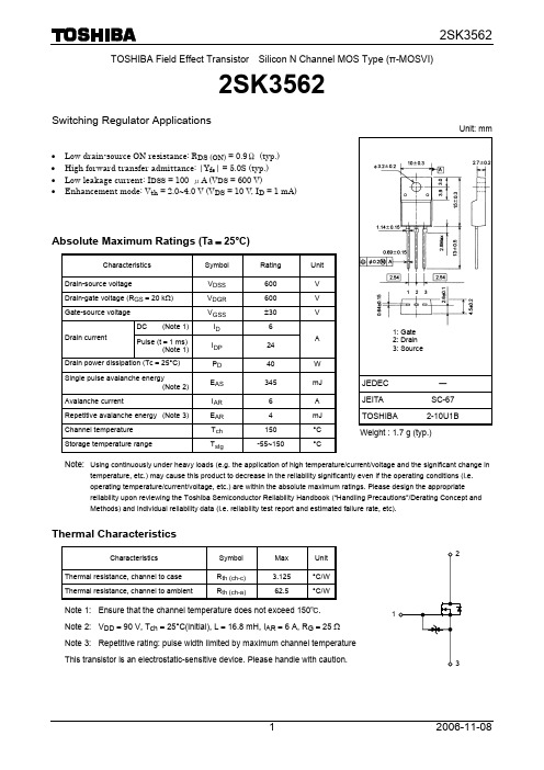
1: Gate 2: Drain 3: Source
5
Tc = 25°C
PULSE TEST
3
1
0.5 10
0.3
5
3
1
VGS = 0, −1 V
0.1
0
−0.2 −0.4 −0.6 −0.8
−1
−1.2
DRAIN-SOURCE VOLTAGE VDS (V)
CAPACITANCE C (pF)
10000 1000
CAPACITANCE – VDS
Ciss
1 VDS = 10 V ID = 1 mA
PULSE TEST
0
−80
−40
0
40
80
120
160
CASE TEMPERATURE Tc (°C)
PD – Tc
50
40 30
20
10
0
0
40
80
120
160
200
CASE TEMPERATURE Tc (°C)
DRAIN-SOURCE VOLTAGE VDS (V)
Thermal Characteristics
2SK2586中文资料

2SK2586Silicon N-Channel MOS FETADE-208-358 C4th. EditionApplicationHigh speed power switchingFeatures• Low on-resistance• R DS(on) = 7 m typ.• High speed switching• 4 V gate drive device can be driven from 5 V sourceOutline2SK25862Absolute Maximum Ratings (Ta = 25°C)ItemSymbol Ratings Unit Drain to source voltage V DSS 60V Gate to source voltage V GSS ±20V Drain current I D *260A Drain peak currentI D(pulse)*1240A Body to drain diode reverse drain current I DR *260A Avalanche current I AP *345A Avalanche energy E AR *3174mJ Channel dissipation Pch*2125W Channel temperature Tch 150°C Storage temperatureTstg–55 to +150°CNotes: 1.PW ≤ 10 µs, duty cycle ≤ 1 %2.Value at Tc = 25°C3.Value at Tch = 25°C, Rg ≥ 50 Ω2SK25863Electrical Characteristics (Ta = 25°C)ItemSymbol Min Typ Max Unit Test Conditions Drain to source breakdown voltageV (BR)DSS 60——V I D = 10 mA, V GS = 0Gate to source breakdown voltageV (BR)GSS ±20——V I G = ±100 µA, V DS = 0Gate to source leak current I GSS ——±10µA V GS = ±16 V, V DS = 0Zero gate voltage drain current I DSS——100µA V DS = 60 V, V GS = 0Gate to source cutoff voltage V GS(off) 1.0— 2.0V I D = 1 mA, V DS = 10 V Static drain to source on state resistanceR DS(on)—710m ΩI D = 30 A V GS = 10 V*1—1016m ΩI D = 30 A V GS = 4 V*1Forward transfer admittance |y fs |3560—S I D = 30 A V DS = 10 V*1Input capacitance Ciss —3550—pF V DS = 10 V Output capacitanceCoss —1760—pF V GS = 0Reverse transfer capacitance Crss —500—pF f = 1 MHz Turn-on delay time t d(on)—35—ns I D = 30 A Rise timet r —260—ns V GS = 10 V Turn-off delay time t d(off)—480—ns R L = 1.0 ΩFall timet f —370—ns Body to drain diode forward voltageV DF —0.94—V I F = 60 A, V GS = 0Body to drain diode reverse recovery time t rr—140—nsI F = 60 A, V GS = 0diF / dt = 50 A / µs Note:1.Pulse TestSee characteristic curves of 2SK2529.2SK25864Hitachi CodeJEDECEIAJWeight (reference value)TO-3P—Conforms5.0 gUnit: mmCautions1.Hitachi neither warrants nor grants licenses of any rights of Hitachi’s or any third party’s patent,copyright, trademark, or other intellectual property rights for information contained in this document.Hitachi bears no responsibility for problems that may arise with third party’s rights, includingintellectual property rights, in connection with use of the information contained in this document.2.Products and product specifications may be subject to change without notice. Confirm that you have received the latest product standards or specifications before final design, purchase or use.3.Hitachi makes every attempt to ensure that its products are of high quality and reliability. However,contact Hitachi’s sales office before using the product in an application that demands especially high quality and reliability or where its failure or malfunction may directly threaten human life or cause risk of bodily injury, such as aerospace, aeronautics, nuclear power, combustion control, transportation,traffic, safety equipment or medical equipment for life support.4.Design your application so that the product is used within the ranges guaranteed by Hitachi particularly for maximum rating, operating supply voltage range, heat radiation characteristics, installationconditions and other characteristics. Hitachi bears no responsibility for failure or damage when used beyond the guaranteed ranges. Even within the guaranteed ranges, consider normally foreseeable failure rates or failure modes in semiconductor devices and employ systemic measures such as fail-safes, so that the equipment incorporating Hitachi product does not cause bodily injury, fire or other consequential damage due to operation of the Hitachi product.5.This product is not designed to be radiation resistant.6.No one is permitted to reproduce or duplicate, in any form, the whole or part of this document without written approval from Hitachi.7.Contact Hitachi’s sales office for any questions regarding this document or Hitachi semiconductor products.Hitachi, Ltd.Semiconductor & Integrated Circuits.Nippon Bldg., 2-6-2, Ohte-machi, Chiyoda-ku, Tokyo 100-0004, Japan Tel: Tokyo (03) 3270-2111 Fax: (03) 3270-5109Copyright ' Hitachi, Ltd., 1999. All rights reserved. Printed in Japan.Hitachi Asia Pte. Ltd.16 Collyer Quay #20-00Hitachi TowerSingapore 049318Tel: 535-2100Fax: 535-1533URLNorthAmerica : http:/Europe : /hel/ecg Asia (Singapore): .sg/grp3/sicd/index.htm Asia (Taiwan): /E/Product/SICD_Frame.htm Asia (HongKong): /eng/bo/grp3/index.htm Japan : http://www.hitachi.co.jp/Sicd/indx.htmHitachi Asia Ltd.Taipei Branch Office3F, Hung Kuo Building. No.167, Tun-Hwa North Road, Taipei (105)Tel: <886> (2) 2718-3666Fax: <886> (2) 2718-8180Hitachi Asia (Hong Kong) Ltd.Group III (Electronic Components)7/F., North Tower, World Finance Centre,Harbour City, Canton Road, Tsim Sha Tsui,Kowloon, Hong Kong Tel: <852> (2) 735 9218Fax: <852> (2) 730 0281 Telex: 40815 HITEC HXHitachi Europe Ltd.Electronic Components Group.Whitebrook ParkLower Cookham Road MaidenheadBerkshire SL6 8YA, United Kingdom Tel: <44> (1628) 585000Fax: <44> (1628) 778322Hitachi Europe GmbHElectronic components Group Dornacher Stra§e 3D-85622 Feldkirchen, Munich GermanyTel: <49> (89) 9 9180-0Fax: <49> (89) 9 29 30 00Hitachi Semiconductor (America) Inc.179 East Tasman Drive,San Jose,CA 95134 Tel: <1> (408) 433-1990Fax: <1>(408) 433-0223For further information write to:。
2SK3271-01中文资料
Drain-Source Breakdown-Voltage
BV DSS
ID=1mA
VGS=0V
Gate Threshhold Voltage
V GS(th)
பைடு நூலகம்
ID=10mA
VDS=VGS
Zero Gate Voltage Drain Current
I DSS
VDS=60V
Tch=25°C
VGS=0V
Min. Typ. Max. Unit 35,0 °C/W
0,806 °C/W
元器件交易网
N-channel MOS-FET
60V 6,5mΩ ±80A 135W
> Characteristics
Typical Output Characteristics
ID=f(VDS); 80µs pulse test; TC=25°C
700
50
200
150
135
100
1,0
85
0,25
S pF pF pF ns ns ns ns A 1,5 V ns µC
- Thermal Characteristics Item Thermal Resistance
Symbol R th(ch-a) R th(ch-c)
Test conditions channel to ambient channel to case
155
W
150
°C
-55 ~ +150
°C
* L=0,65.4uH, VCC=24V
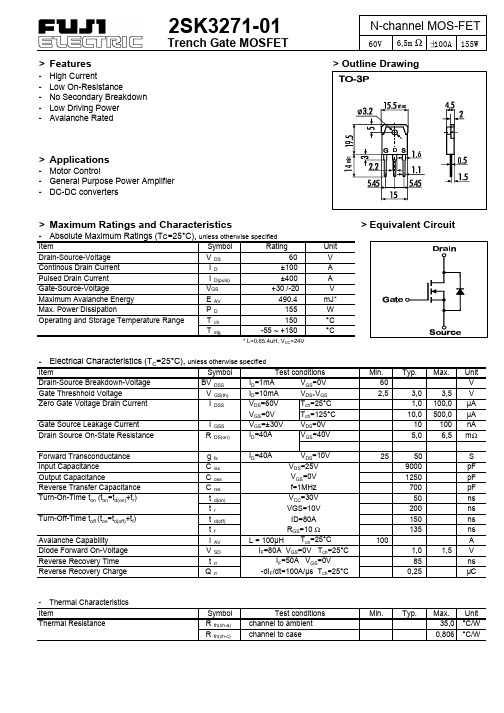
> Equivalent Circuit
- Electrical Characteristics (TC=25°C), unless otherwise specified
2SK3356资料
DATA SHEETDocument No.D14133EJ1V0DS00 (1st edition)The information in this document is subject to change without notice. Before using this document, pleaseconfirm that this is the latest version.Not all devices/types available in every country. Please check with local NEC representative for availability and additional information.The mark 5 shows major revised points.DESCRIPTIONThe 2SK3356 is N-channel MOS Field Effect Transistor designed for high current switching applications.FEATURES•Super low on-state resistance:R DS(on)1 = 8.0 m Ω MAX. (V GS = 10 V, I D = 38 A)R DS(on)2 = 12 m Ω MAX. (V GS = 4 V, I D = 38 A)•Low C iss : C iss = 6300 pF TYP.•Built-in gate protection diodeABSOLUTE MAXIMUM RATINGS (T A = 25°C)Drain to Source Voltage V DSS 60V Gate to Source Voltage V GSS(AC)±20V Drain Current (DC)I D(DC)±75A Drain Current (pulse) Note1I D(pulse)±300A Total Power Dissipation (T C = 25°C)P T 130W Total Power Dissipation (T A = 25°C)P T 3.0W Channel Temperature T ch 150°C Storage TemperatureT stg –55 to +150°C Single Avalanche Current Note2I AS 55A Single Avalanche Energy Note2E AS302mJNotes 1.PW ≤ 10 µs, Duty cycle ≤ 1 %2. Starting T ch = 25 °C, R G = 25 Ω, V GS = 20 V → 0 VTHERMAL RESISTANCEChannel to Case Rth(ch-C)0.93°C/W Channel to AmbientRth(ch-A)41.7°C/WORDERING INFORMATIONPART NUMBERPACKAGE 2SK3356TO-3P55555552ELECTRICAL CHARACTERISTICS (T A = 25 °C)CHARACTERISTICSSYMBOL TEST CONDITIONSMIN.TYP.MAX.UNIT Drain to Source On-state ResistanceR DS(on)1V GS = 10 V, I D = 38 A 6.38.0m ΩR DS(on)2V GS = 4 V, I D = 38 A 8.012m ΩGate to Source Cut-off Voltage V GS(off)V DS = 10 V, I D = 1 mA 1.5 2.0 2.5VForward Transfer Admittance | y fs|V DS = 10 V, I D = 38 A 3557SDrain Leakage CurrentI DSS V DS = 60 V, V GS = 0 V 10µA Gate to Source Leakage Current I GSS V GS = ±20 V, V DS = 0V±10µA Input Capacitance C iss V DS = 10 V, V GS = 0 V, f = 1 MHz6300pF Output CapacitanceC oss 1000pF Reverse Transfer Capacitance C rss 490pF Turn-on Delay Time t d(on)ID = 38 A, V GS(on) = 10 V, V DD = 30 V,90ns Rise Timet r R G = 10 Ω1100ns Turn-off Delay Time t d(off)300ns Fall Timet f 400ns Total Gate Charge Q G I D = 75 A , V DD = 48 V, V GS = 10 V 106nC Gate to Source Charge Q GS 20nC Gate to Drain Charge Q GD 30nC Body Diode Forward Voltage V F(S-D)I F = 75 A, V GS = 0 V 1.0V Reverse Recovery Time t rr I F = 75 A, V GS = 0 V,55ns Reverse Recovery ChargeQ rrdi/dt = 100 A/µs100nC5TEST CIRCUIT 3 GATE CHARGEV GS = 20 → 0 TEST CIRCUIT 1 AVALANCHE CAPABILITYL DDTEST CIRCUIT 2 SWITCHING TIMEL DDτ = 1 µsDuty Cycle ≤ 1 %3PACKAGE DRAWING (Unit: mm)Remark The diode connected between the gate and source of the transistor serves as a protector against ESD.When this device actually used, an additional protection circuit is externally required if a voltage exceeding the rated voltage may be applied to this device.TO-3P (MP-88)EQUIVALENT CIRCUITBody DiodeDiodeDrain• The information in this document is subject to change without notice. Before using this document, please confirm that this is the latest version.• No part of this document may be copied or reproduced in any form or by any means without the prior written consent of NEC Corporation. NEC Corporation assumes no responsibility for any errors which may appear in this document.• NEC Corporation does not assume any liability for infringement of patents, copyrights or other intellectual propertyrights of third parties by or arising from use of a device described herein or any other liability arising from useof such device. No license, either express, implied or otherwise, is granted under any patents, copyrights or otherintellectual property rights of NEC Corporation or others.• Descriptions of circuits, software, and other related information in this document are provided for illustrative purposes in semiconductor product operation and application examples. The incorporation of these circuits,software, and information in the design of the customer's equipment shall be done under the full responsibilityof the customer. NEC Corporation assumes no responsibility for any losses incurred by the customer or third parties arising from the use of these circuits, software, and information.• While NEC Corporation has been making continuous effort to enhance the reliability of its semiconductor devices,the possibility of defects cannot be eliminated entirely. To minimize risks of damage or injury to persons orproperty arising from a defect in an NEC semiconductor device, customers must incorporate sufficient safety measures in its design, such as redundancy, fire-containment, and anti-failure features.• NEC devices are classified into the following three quality grades:"Standard", "Special", and "Specific". The Specific quality grade applies only to devices developed based on acustomer designated "quality assurance program" for a specific application. The recommended applications ofa device depend on its quality grade, as indicated below. Customers must check the quality grade of each devicebefore using it in a particular application.Standard: Computers, office equipment, communications equipment, test and measurement equipment,audio and visual equipment, home electronic appliances, machine tools, personal electronic equipment and industrial robotsSpecial: Transportation equipment (automobiles, trains, ships, etc.), traffic control systems, anti-disastersystems, anti-crime systems, safety equipment and medical equipment (not specifically designed for life support)Specific: Aircraft, aerospace equipment, submersible repeaters, nuclear reactor control systems, lifesupport systems or medical equipment for life support, etc.The quality grade of NEC devices is "Standard" unless otherwise specified in NEC's Data Sheets or Data Books. If customers intend to use NEC devices for applications other than those specified for Standard quality grade, they should contact an NEC sales representative in advance.M7 98. 8。
2SK1941中文资料

- Electrical Characteristics (TC=25°C), unless otherwise specified
Item
Symbol
Test conditions
Drain-Source Breakdown-Voltage
V (BR)DSS ID=1mA
Symbol R th(ch-a) R th(ch-c)
Test conditions channel to air channel to case
Min. Typ. Max. Unit 30 °C/W 1,25 °C/W
FUJI ELECTRIC GmbH; Lyoner Straße 26; D-60528 Frankfurt; Tel: 069-66 90 29-0; Fax: 069-66 90 29-56
VGS=±30V VDS=0V
Drain Source On-State Resistance
R DS(on)
ID=8A
VGS=10V
Forward Transconductance
g fs
ID=8A
VDS=25V
Input Capacitance
C iss
VDS=25V
Output Capacitance
C oss
VGS=0V
Reverse Transfer Capacitance
C rss
f=1MHz
Turn-On-Time ton (ton=td(on)+tr)
t d(on)
VCC=300V
tr
ID=8A
Turn-Off-Time toff (ton=td(off)+tf)
2SK1647L-E中文资料
2SK1647(L), 2SK1647(S)
Silicon N Channel MOS FET
REJ03G0963-0200 (Previous: ADE-208-1306) Rev.2.00 Sep 07, 2005
Application
High speed power switching
0.1
0.05 0.02
ls 1 0.0 t Pu o h 1S e
1.0
TC = 25°C
θch–c (t) = γS (t) • θch–c θch–c = 2.50°C/W, TC = 25°C PDM PW D = PW T
0.
0.01 10 µ
0
0.4
0.8
1.2
1.6
2.0
Source to Drain Voltage VSD (V)
Normalized Transient Thermal Impedance γS (t)
Normalized Transient Thermal Impedance vs. Pulse Width
3 D=1 0.5 0.3 0.1 0.2
50 Pulse Test 40
Gate to Source Voltage VGS (V) Static Drain to Source on State Resistance vs. Drain Current
50 Pulse Test 20 10 5 VGS = 10 V 15 V
Drain to Source Saturation Voltage VDS (on) (V)
Drain to Source Voltage VDS (V)
2SK2608中文资料

TOSHIBA Field Effect Transistor Silicon N Channel MOS Type (π−MOSIII)2SK2608Switching Regulator Applicationsz Low drain −source ON resistance : R DS (ON) = 3.73 Ω (typ.) z High forward transfer admittance : |Y fs |= 2.6 S (typ.)z Low leakage current : I DSS = 100 μA (max) (V DS = 720 V) z Enhancement mode : V th = 2.0~4.0 V (V DS = 10 V, I D = 1 mA)Absolute Maximum Ratings (Ta = 25°C)Characteristics Symbol Rating UnitDrain −source voltageV DSS 900 VDrain −gate voltage (R GS = 20 k Ω) V DGR 900 V Gate −source voltage V GSS ±30 V DC (Note 1) I D 3 A Drain currentPulse (Note 1)I DP 9A Drain power dissipation (Tc = 25°C)P D 100 WSingle pulse avalanche energy(Note 2) E AS 295mJ Avalanche currentI AR 3 ARepetitive avalanche energy (Note 3) E AR 10.0 mJ Channel temperature T ch 150 °C Storage temperature rangeT stg−55~150 °CNote: Using continuously under heavy loads (e.g. the application of high temperature/current/voltage and the significant change intemperature, etc.) may cause this product to decrease in the reliability significantly even if the operating conditions (i.e. operating temperature/current/voltage, etc.) are within the absolute maximum ratings. Please design the appropriate reliability upon reviewing the Toshiba Semiconductor Reliability Handbook (“Handling Precautions”/Derating Concept and Methods) and individual reliability data (i.e. reliability test report and estimated failure rate, etc).Thermal CharacteristicsCharacteristics Symbol Max UnitThermal resistance, channel to case R th (ch −c) 1.25 °C / W Thermal resistance, channel to ambientR th (ch −a)83.3°C / WNote 1: Ensure that the channel temperature does not exceed 150°C. Note 2: V DD = 90 V, T ch = 25°C (initial), L = 60.0 mH, R G = 25 Ω, I AR = 3 A Note 3: Repetitive rating: pulse width limited by maximum channel temperature This transistor is an electrostatic-sensitive device. Please handle with caution.Unit: mmJEDEC TO-220AB JEITA SC-46 TOSHIBA 2-10P1B Weight: 2.0 g (typ.)Electrical Characteristics (Ta = 25°C)Characteristics SymbolTest ConditionMin Typ. Max Unit Gate leakage currentI GSS V GS = ±30 V, V DS = 0 V — — ±10μA Gate −source breakdown voltage V (BR) GSS I G = ±10 μA, V DS = 0 V ±30 — — V Drain cut −off currentI DSS V DS = 720 V, V GS = 0 V — — 100μA Drain −source breakdown voltage V (BR) DSS I D = 10 mA, V GS = 0 V 900 — — V Gate threshold voltage V th V DS = 10 V, I D = 1 mA 2.0 — 4.0 V Drain −source ON resistance R DS (ON)V GS = 10 V, I D = 1.5 A— 3.73 4.3 Ω Forward transfer admittance |Y fs | V DS = 20 V, I D = 1.5 A0.652.6—SInput capacitanceC iss — 750 —Reverse transfer capacitance C rss — 10 — Output capacitanceC ossV DS = 25 V, V GS = 0 V, f = 1 MHz — 70 —pF Rise timet r — 15 —Turn −on timet on — 55 —Fall timet f — 30 — Switching timeTurn −off timet off— 110 —nsTotal gate charge (gate −sourceplus gate −drain) Q g —25 — Gate −source charge Q gs — 13 — Gate −drain (“miller”) ChargeQ gdV DD ≈ 400 V, V GS = 10 V, I D = 3 A — 12 —nCSource −Drain Ratings and Characteristics (Ta = 25°C)Characteristics SymbolTest ConditionMin Typ. Max UnitContinuous drain reverse current(Note 1)I DR —— — 3 A Pulse drain reverse current(Note 1) I DRP —— — 9 A Forward voltage (diode) V DSF I DR = 3 A, V GS = 0 V——−1.9VReverse recovery time t rr — 1200 — ns Reverse recovery chargeQ rrI DR = 3 A, V GS = 0 V, dI DR / dt = 100 A / μs— 8.5 — μCMarkinglead (Pb)-free package or lead (Pb)-free finish.K2608⎟⎠⎞⎜⎝⎛−⋅⋅⋅=DD VDSS VDSS AS V B B I L 21E 2R G = 25 ΩV DD = 90 V , L = 60 mHRESTRICTIONS ON PRODUCT USE20070701-EN •The information contained herein is subject to change without notice.•TOSHIBA is continually working to improve the quality and reliability of its products. Nevertheless, semiconductor devices in general can malfunction or fail due to their inherent electrical sensitivity and vulnerability to physical stress. It is the responsibility of the buyer, when utilizing TOSHIBA products, to comply with the standards of safety in making a safe design for the entire system, and to avoid situations in which a malfunction or failure of such TOSHIBA products could cause loss of human life, bodily injury or damage to property.In developing your designs, please ensure that TOSHIBA products are used within specified operating ranges as set forth in the most recent TOSHIBA products specifications. Also, please keep in mind the precautions and conditions set forth in the “Handling Guide for Semiconductor Devices,” or “TOSHIBA Semiconductor Reliability Handbook” etc.• The TOSHIBA products listed in this document are intended for usage in general electronics applications (computer, personal equipment, office equipment, measuring equipment, industrial robotics, domestic appliances, etc.).These TOSHIBA products are neither intended nor warranted for usage in equipment that requires extraordinarily high quality and/or reliability or a malfunction or failure of which may cause loss of human life or bodily injury (“Unintended Usage”). Unintended Usage include atomic energy control instruments, airplane or spaceship instruments, transportation instruments, traffic signal instruments, combustion control instruments, medical instruments, all types of safety devices, etc.. Unintended Usage of TOSHIBA products listed in his document shall be made at the customer’s own risk.•The products described in this document shall not be used or embedded to any downstream products of which manufacture, use and/or sale are prohibited under any applicable laws and regulations.• The information contained herein is presented only as a guide for the applications of our products. No responsibility is assumed by TOSHIBA for any infringements of patents or other rights of the third parties which may result from its use. No license is granted by implication or otherwise under any patents or other rights of TOSHIBA or the third parties.• Please contact your sales representative for product-by-product details in this document regarding RoHS compatibility. Please use these products in this document in compliance with all applicable laws and regulations that regulate the inclusion or use of controlled substances. Toshiba assumes no liability for damage or losses occurring as a result of noncompliance with applicable laws and regulations.。
2SK2551_06资料
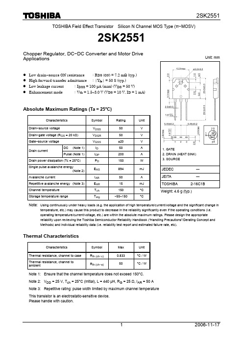
TOSHIBA Field Effect Transistor Silicon N Channel MOS Type (π−MOSV)2SK2551Chopper Regulator, DC −DC Converter and Motor Drive Applicationsz Low drain −source ON resistance : R DS (ON) = 7.2 m Ω (typ.) z High forward transfer admittance : |Y fs | = 50 S (typ.)z Low leakage current : I DSS = 100 μA (max) (V DS = 50 V) z Enhancement mode : V th = 1.5~3.0 V (V DS = 10 V, I D = 1 mA)Absolute Maximum Ratings (Ta = 25°C)Characteristics Symbol Rating UnitDrain −source voltageV DSS 50 VDrain −gate voltage (R GS = 20 k Ω) V DGR 50 VGate −source voltage V GSS ±20 VDC (Note 1) I D 50 A Drain currentPulse (Note 1)I DP 200A Drain power dissipation (Tc = 25°C)P D150 WSingle pulse avalanche energy(Note 2) E AS 894mJ Avalanche currentI AR 50 ARepetitive avalanche energy (Note 3) E AR 15 mJ Channel temperature T ch 150 °C Storage temperature rangeT stg−55~150 °CNote: Using continuously under heavy loads (e.g. the application of high temperature/current/voltage and the significant change intemperature, etc.) may cause this product to decrease in the reliability significantly even if the operating conditions (i.e. operating temperature/current/voltage, etc.) are within the absolute maximum ratings. Please design the appropriate reliability upon reviewing the Toshiba Semiconductor Reliability Handbook (“Handling Precautions”/Derating Concept and Methods) and individual reliability data (i.e. reliability test report and estimated failure rate, etc).Thermal CharacteristicsCharacteristics Symbol Max UnitThermal resistance, channel to case R th (ch −c)0.833°C / W Thermal resistance, channel to ambientR th (ch −a) 50°C / WNote 1: Ensure that the channel temperature does not exceed 150°C. Note 2: V DD = 25 V, T ch = 25°C (initial), L = 440 μH, R G = 25 Ω, I AR = 50 A Note 3: Repetitive rating: pulse width limited by maximum channel temperature This transistor is an electrostatic-sensitive device. Please handle with caution.Unit: mm1. GATE2. DRAIN (HEAT SINK)3. SOURCEJEDEC ― JEITA ―TOSHIBA 2-16C1BWeight: 4.6 g (typ.)Electrical Characteristics (Ta = 25°C)Characteristics SymbolTest ConditionMin Typ. Max Unit Gate leakage current I GSS V GS = ±16 V, V DS = 0 V — — ±10μA Drain cut −off currentI DSS V DS = 50 V, V GS = 0 V — — 100μA Drain −source breakdown voltage V (BR) DSSI D = 10 mA, V GS = 0 V 50 — — V Gate threshold voltage V th V DS = 10 V, I D = 1 mA 1.5 — 3.0 V Drain −source ON resistance R DS (ON)V GS = 10 V, I D = 25 A— 7.2 11 m Ω Forward transfer admittance |Y fs | V DS = 10 V, I D = 25 A3050—SInput capacitanceC iss — 4000 —Reverse transfer capacitance C rss — 800 — Output capacitanceC ossV DS = 10 V, V GS = 0 V, f = 1 MHz — 2000 —pF Rise timet r — 25 —Turn −on timet on — 40 —Fall timet f — 120 —Switching timeTurn −off timet off— 360 —nsTotal gate charge (Gate −sourceplus gate −drain) Q g —130 — Gate −source charge Q gs — 90 — Gate −drain (“miller”) chargeQ gdV DD ≈ 40 V, V GS = 10 V, I D = 50 A — 40 —nCSource −Drain Ratings and Characteristics (Ta = 25°C)Characteristics SymbolTest ConditionMin Typ. Max UnitContinuous drain reverse current(Note 1) I DR —— — 50 A Pulse drain reverse current(Note 1) I DRP — — — 200 A Forward voltage (diode) V DSFI DR = 50 A, V GS = 0 V — — −1.7VReverse recovery time t rr — 140 — ns Reverse recovered chargeQ rrI DR= 50 A, V GS= 0 V dI DR / dt = 50 A / μs— 77 — μCMarkingK2551lead (Pb)-free package or lead (Pb)-free finish.⎟⎠⎞⎜⎝⎛−⋅⋅⋅=DD VDSS VDSS B I L 1AS E 2R G = 25 ΩV DD = 25 V , L = 440 μHRESTRICTIONS ON PRODUCT USE20070701-EN •The information contained herein is subject to change without notice.•TOSHIBA is continually working to improve the quality and reliability of its products. Nevertheless, semiconductor devices in general can malfunction or fail due to their inherent electrical sensitivity and vulnerability to physical stress. It is the responsibility of the buyer, when utilizing TOSHIBA products, to comply with the standards of safety in making a safe design for the entire system, and to avoid situations in which a malfunction or failure of such TOSHIBA products could cause loss of human life, bodily injury or damage to property.In developing your designs, please ensure that TOSHIBA products are used within specified operating ranges as set forth in the most recent TOSHIBA products specifications. Also, please keep in mind the precautions and conditions set forth in the “Handling Guide for Semiconductor Devices,” or “TOSHIBA Semiconductor Reliability Handbook” etc.• The TOSHIBA products listed in this document are intended for usage in general electronics applications (computer, personal equipment, office equipment, measuring equipment, industrial robotics, domestic appliances, etc.).These TOSHIBA products are neither intended nor warranted for usage in equipment that requires extraordinarily high quality and/or reliability or a malfunction or failure of which may cause loss of human life or bodily injury (“Unintended Usage”). Unintended Usage include atomic energy control instruments, airplane or spaceship instruments, transportation instruments, traffic signal instruments, combustion control instruments, medical instruments, all types of safety devices, etc.. Unintended Usage of TOSHIBA products listed in his document shall be made at the customer’s own risk.•The products described in this document shall not be used or embedded to any downstream products of which manufacture, use and/or sale are prohibited under any applicable laws and regulations.• The information contained herein is presented only as a guide for the applications of our products. No responsibility is assumed by TOSHIBA for any infringements of patents or other rights of the third parties which may result from its use. No license is granted by implication or otherwise under any patents or other rights of TOSHIBA or the third parties.• Please contact your sales representative for product-by-product details in this document regarding RoHS compatibility. Please use these products in this document in compliance with all applicable laws and regulations that regulate the inclusion or use of controlled substances. Toshiba assumes no liability for damage or losses occurring as a result of noncompliance with applicable laws and regulations.。
- 1、下载文档前请自行甄别文档内容的完整性,平台不提供额外的编辑、内容补充、找答案等附加服务。
- 2、"仅部分预览"的文档,不可在线预览部分如存在完整性等问题,可反馈申请退款(可完整预览的文档不适用该条件!)。
- 3、如文档侵犯您的权益,请联系客服反馈,我们会尽快为您处理(人工客服工作时间:9:00-18:30)。
V GS =-30V T ch 150°C L=1.74mH V CC =60V *1VDS 600V *2T a=25°C Tc=25°CItemSymbol Ratings Unit Remarks Drain-source voltage V DS 600V DSX 600Continuous drain current I D ±16Pulsed drain current I D(puls]±64Gate-source voltage V GS ±30Non-RepetitiveI AS 16Maximum avalanche current Non-RepetitiveE AS 242.7Maximum avalanche energy Maximum Drain-Source dV/dt dV DS /dt 20Peak diode recovery dV/dt dV/dt 5Max. power dissipation P D 2.02270Operating and storage T ch +150temperature rangeT stgElectrical characteristics (T c =25°C unless otherwise specified)2SK3686-01FUJI POWER MOSFETN-CHANNEL SILICON POWER MOSFETFeaturesHigh speed switching Low on-resistance No secondary breadown Low driving power Avalanche-proofApplicationsSwitching regulators DC-DC converters Maximum ratings and characteristic Absolute maximum ratings(Tc=25°C unless otherwise specified)Zero gate voltage drain current I DSS V DS =600V V GS =0V V DS =480V V GS =0V V GS =±30V I D =8A V GS =10V I D =8A V DS =25V V CC =300V I D =8A V GS =10V R GS =10 ΩMin. Typ. Max. UnitsV V µA nA ΩS pFnCA V µs µCnsSymbol V (BR)DSS V GS(th)I GSS R DS(on)g fs C iss C oss C rss td (on)t rtd (off)t f Q G Q GS Q GD I AV V SD t rr Q rrItemDrain-source breakdown voltaget Gate threshold voltage Gate-source leakage currentDrain-source on-state resistance Forward transcondutance Input capacitance Output capacitanceReverse transfer capacitance Turn-on time t on Turn-off time t offTotal Gate Charge Gate-Source Charge Gate-Drain Charge Avalanche capabilityDiode forward on-voltage Reverse recovery time Reverse recovery charge Test Conditions I D = 250µA V GS =0V I D = 250µA V DS =V GS T ch =25°C T ch =125°C V DS =0V V DS =25V V GS =0V f=1MHzV CC =300V I D =16A V GS =10VL=1.74mH T ch =25°CI F =16A V GS =0V T ch =25°C I F =16A V GS =0V-di/dt=100A/µs T ch =25°CV V A A VA mJ kV/skV/µs W °C °C6003.05.025*********.420.576.513159023902003008122943.516245887812345112181015161.00 1.500.687.8-55 to +150Outline Drawings [mm]Super FAP-G Series200311<=<=*1 See to Avalanche Energy Graph*2 I F -I D , -di/dt=50A/µs, V CC BV DSS , Tch 150°C <=<=<=Characteristics4812162024010203040507V20V 10V 8V 6.5VVGS=6.0VI D [A ]VDS [V]Typical Output CharacteristicsID=f(VDS):80 µs pulse test,Tch=25 °C2550751001251500100200300400P D [W ]Tc [°C]0123456789100.1110100I D [A ]VGS[V]0.11101000.1110100g f s [S ]ID [A]Typical Transconductancegfs=f(ID):80 µs pulse test,VDS=25V,Tch=25°C01020300.00.10.20.30.40.50.60.70.80.91.0 R D S (o n ) [Ω ]ID [A]Typical Drain-Source on-state Resistance-50-252550751001251500.00.10.20.30.40.50.60.70.80.91.01.11.21.31.41.5R D S (o n ) [ Ω ]Tch [°C]Drain-Source On-state Resistance-50-252550751001251500.00.51.01.52.02.53.03.54.04.55.05.56.06.57.0Gate Threshold Voltage vs. TchV G S (t h ) [V ]Tch [°C]1020304050602468101214Qg [nC]V G S [V ]1010110210310C [p F ]VDS [V]Typical Capacitance0.000.250.500.75 1.00 1.25 1.50 1.75 2.00 2.25 2.500.1110100I F [A ]VSD [V]Typical Forward Characteristics of Reverse Diode IF=f(VSD):80 µs pulse test,Tch=25 °C10-11010110210101102103t [n s ]ID [A]02550751001251500100200300400500600700E A V [m J ]starting Tch [°C]Maximum Avalanche Energy vs. starting Tchhttp://www.fujielectric.co.jp/fdt/scd/10-810-710-610-510-410-310-210101010A v a l a n c h e C u r r e n t I A V [A ]t AV [sec]10-610-510-410-310-210-11010-310-210-110101Maximum Transient Thermal Impedance Zth(ch-c)=f(t):D=0Z t h (c h -c ) [°C /W ]t [sec]。