MAX2650EUS中文资料
MAX13085EESA-T中文资料

General DescriptionThe MAX13080E–MAX13089E +5.0V, ±15kV ESD-protect-ed, RS-485/RS-422 transceivers feature one driver and one receiver. These devices include fail-safe circuitry,guaranteeing a logic-high receiver output when receiver inputs are open or shorted. The receiver outputs a logic-high if all transmitters on a terminated bus are disabled (high impedance). The MAX13080E–MAX13089E include a hot-swap capability to eliminate false transitions on the bus during power-up or hot insertion.The MAX13080E/MAX13081E/MAX13082E feature reduced slew-rate drivers that minimize EMI and reduce reflections caused by improperly terminated cables, allowing error-free data transmission up to 250kbps. The MAX13083E/MAX13084E/MAX13085E also feature slew-rate-limited drivers but allow transmit speeds up to 500kbps. The MAX13086E/MAX13087E/MAX13088E driver slew rates are not limited, making transmit speeds up to 16Mbps possible. The MAX13089E slew rate is pin selectable for 250kbps,500kbps, and 16Mbps.The MAX13082E/MAX13085E/MAX13088E are intended for half-duplex communications, and the MAX13080E/MAX13081E/MAX13083E/MAX13084E/MAX13086E/MAX13087E are intended for full-duplex communica-tions. The MAX13089E is selectable for half-duplex or full-duplex operation. It also features independently programmable receiver and transmitter output phase through separate pins.The MAX13080E–MAX13089E transceivers draw 1.2mA of supply current when unloaded or when fully loaded with the drivers disabled. All devices have a 1/8-unit load receiver input impedance, allowing up to 256transceivers on the bus.The MAX13080E/MAX13083E/MAX13086E/MAX13089E are available in 14-pin PDIP and 14-pin SO packages.The MAX13081E/MAX13082E/MAX13084E/MAX13085E/MAX13087E/MAX13088E are available in 8-pin PDIP and 8-pin SO packages. The devices operate over the com-mercial, extended, and automotive temperature ranges.ApplicationsUtility Meters Lighting Systems Industrial Control Telecom Security Systems Instrumentation ProfibusFeatures♦+5.0V Operation♦Extended ESD Protection for RS-485/RS-422 I/O Pins±15kV Human Body Model ♦True Fail-Safe Receiver While Maintaining EIA/TIA-485 Compatibility ♦Hot-Swap Input Structures on DE and RE ♦Enhanced Slew-Rate Limiting Facilitates Error-Free Data Transmission(MAX13080E–MAX13085E/MAX13089E)♦Low-Current Shutdown Mode (Except MAX13081E/MAX13084E/MAX13087E)♦Pin-Selectable Full-/Half-Duplex Operation (MAX13089E)♦Phase Controls to Correct for Twisted-Pair Reversal (MAX13089E)♦Allow Up to 256 Transceivers on the Bus ♦Available in Industry-Standard 8-Pin SO PackageMAX13080E–MAX13089E+5.0V , ±15kV ESD-Protected, Fail-Safe, Hot-Swap, RS-485/RS-422 Transceivers________________________________________________________________Maxim Integrated Products 1Ordering Information19-3590; Rev 1; 4/05For pricing, delivery, and ordering information,please contact Maxim/Dallas Direct!at 1-888-629-4642, or visit Maxim’s website at .Selector Guide, Pin Configurations, and Typical Operating Circuits appear at end of data sheet.Ordering Information continued at end of data sheet.M A X 13080E –M A X 13089E+5.0V , ±15kV ESD-Protected, Fail-Safe, Hot-Swap, RS-485/RS-422 Transceivers 2_______________________________________________________________________________________ABSOLUTE MAXIMUM RATINGSDC ELECTRICAL CHARACTERISTICS(V CC = +5.0V ±10%, T A = T MIN to T MAX , unless otherwise noted. Typical values are at V CC = +5.0V and T A = +25°C.) (Note 1)Stresses beyond those listed under “Absolute Maximum Ratings” may cause permanent damage to the device. These are stress ratings only, and functional operation of the device at these or any other conditions beyond those indicated in the operational sections of the specifications is not implied. Exposure to absolute maximum rating conditions for extended periods may affect device reliability.(All Voltages Referenced to GND)Supply Voltage (V CC ).............................................................+6V Control Input Voltage (RE , DE, SLR,H/F , TXP, RXP)......................................................-0.3V to +6V Driver Input Voltage (DI)...........................................-0.3V to +6V Driver Output Voltage (Z, Y, A, B).............................-8V to +13V Receiver Input Voltage (A, B)....................................-8V to +13V Receiver Input VoltageFull Duplex (A, B)..................................................-8V to +13V Receiver Output Voltage (RO)....................-0.3V to (V CC + 0.3V)Driver Output Current.....................................................±250mAContinuous Power Dissipation (T A = +70°C)8-Pin SO (derate 5.88mW/°C above +70°C).................471mW 8-Pin Plastic DIP (derate 9.09mW/°C above +70°C).....727mW 14-Pin SO (derate 8.33mW/°C above +70°C)...............667mW 14-Pin Plastic DIP (derate 10.0mW/°C above +70°C)...800mW Operating Temperature RangesMAX1308_EC_ _.................................................0°C to +75°C MAX1308_EE_ _..............................................-40°C to +85°C MAX1308_EA_ _............................................-40°C to +125°C Junction Temperature......................................................+150°C Storage Temperature Range.............................-65°C to +150°C Lead Temperature (soldering, 10s).................................+300°CMAX13080E–MAX13089E+5.0V , ±15kV ESD-Protected, Fail-Safe, Hot-Swap, RS-485/RS-422 Transceivers_______________________________________________________________________________________3DC ELECTRICAL CHARACTERISTICS (continued)(V CC = +5.0V ±10%, T A = T MIN to T MAX , unless otherwise noted. Typical values are at V CC = +5.0V and T A = +25°C.) (Note 1)M A X 13080E –M A X 13089E+5.0V , ±15kV ESD-Protected, Fail-Safe, Hot-Swap, RS-485/RS-422 Transceivers 4_______________________________________________________________________________________DRIVER SWITCHING CHARACTERISTICSMAX13080E/MAX13081E/MAX13082E/MAX13089E WITH SRL = UNCONNECTED (250kbps)(V CC = +5.0V ±10%, T A = T MIN to T MAX , unless otherwise noted. Typical values are at V CC = +5.0V and T A = +25°C.)RECEIVER SWITCHING CHARACTERISTICSMAX13080E/MAX13081E/MAX13082E/MAX13089E WITH SRL = UNCONNECTED (250kbps)(V CC = +5.0V ±10%, T A = T MIN to T MAX , unless otherwise noted. Typical values are at V CC = +5.0V and T A = +25°C.)MAX13080E–MAX13089E+5.0V , ±15kV ESD-Protected, Fail-Safe, Hot-Swap, RS-485/RS-422 Transceivers_______________________________________________________________________________________5DRIVER SWITCHING CHARACTERISTICSMAX13083E/MAX13084E/MAX13085E/MAX13089E WITH SRL = V CC (500kbps)(V CC = +5.0V ±10%, T A = T MIN to T MAX , unless otherwise noted. Typical values are at V CC = +5.0V and T A = +25°C.)RECEIVER SWITCHING CHARACTERISTICSMAX13083E/MAX13084E/MAX13085E/MAX13089E WITH SRL = V CC (500kbps)(V CC = +5.0V ±10%, T A = T MIN to T MAX , unless otherwise noted. Typical values are at V CC = +5.0V and T A = +25°C.)M A X 13080E –M A X 13089E+5.0V , ±15kV ESD-Protected, Fail-Safe, Hot-Swap, RS-485/RS-422 Transceivers 6_______________________________________________________________________________________DRIVER SWITCHING CHARACTERISTICSMAX13086E/MAX13087E/MAX13088E/MAX13089E WITH SRL = GND (16Mbps)(V CC = +5.0V ±10%, T A = T MIN to T MAX , unless otherwise noted. Typical values are at V CC = +5.0V and T A = +25°C.)RECEIVER SWITCHING CHARACTERISTICSMAX13086E/MAX13087E/MAX13088E/MAX13089E WITH SRL = GND (16Mbps)(V CC = +5.0V ±10%, T A = T MIN to T MAX , unless otherwise noted. Typical values are at V CC = +5.0V and T A = +25°C.)Note 2:∆V OD and ∆V OC are the changes in V OD and V OC , respectively, when the DI input changes state.Note 3:The short-circuit output current applies to peak current just prior to foldback current limiting. The short-circuit foldback outputcurrent applies during current limiting to allow a recovery from bus contention.MAX13080E–MAX13089E+5.0V , ±15kV ESD-Protected, Fail-Safe, Hot-Swap, RS-485/RS-422 Transceivers_______________________________________________________________________________________70.800.901.501.101.001.201.301.401.60-40-10520-253550958011065125SUPPLY CURRENT vs. TEMPERATURETEMPERATURE (°C)S U P P L Y C U R R E N T (m A )0201040305060021345OUTPUT CURRENTvs. RECEIVER OUTPUT-HIGH VOLTAGEM A X 13080E -89E t o c 02OUTPUT HIGH VOLTAGE (V)O U T P U T C U R R E N T (m A )20104030605070021345OUTPUT CURRENTvs. RECEIVER OUTPUT-LOW VOLTAGEM A X 13080E -89E t o c 03OUTPUT LOW VOLTAGE (V)O U T P U T C U R R E N T (m A )4.04.44.24.84.65.25.05.4RECEIVER OUTPUT-HIGH VOLTAGEvs. TEMPERATURETEMPERATURE (°C)O U T P U T H I G H V O L T A G E (V )-40-10520-2535509580110651250.10.70.30.20.40.50.60.8RECEIVER OUTPUT-LOW VOLTAGEvs. TEMPERATURETEMPERATURE (°C)O U T P U T L O W V O L T A G E (V )-40-10520-25355095801106512502040608010012014016012345DRIVER DIFFERENTIAL OUTPUT CURRENT vs. DIFFERENTIAL OUTPUT VOLTAGEDIFFERENTIAL OUTPUT VOLTAGE (V)D I F FE R E N T I A L O U T P U T C U R R E N T (m A )2.02.82.43.63.24.44.04.8DRIVER DIFFERENTIAL OUTPUT VOLTAGE vs. TEMPERATURED I F FE R E N T I A L O U T P U T V O L T A G E (V )-40-10520-253550958011065125TEMPERATURE (°C)40201008060120140180160200-7-5-4-6-3-2-1012354OUTPUT CURRENT vs. TRANSMITTEROUTPUT-HIGH VOLTAGEOUTPUT HIGH VOLTAGE (V)O U T P U T C U R R E N T (m A )60402080100120140160180200042681012OUTPUT CURRENT vs. TRANSMITTEROUTPUT-LOW VOLTAGEOUTPUT-LOW VOLTAGE (V)O U T P U T C U R R E N T (m A )Typical Operating Characteristics(V CC = +5.0V, T A = +25°C, unless otherwise noted.)M A X 13080E –M A X 13089E+5.0V , ±15kV ESD-Protected, Fail-Safe, Hot-Swap, RS-485/RS-422 Transceivers 8_______________________________________________________________________________________21543679810SHUTDOWN CURRENT vs. TEMPERATUREM A X 13080E -89E t o c 10S H U T D O W N C U R R E N T (µA )-40-10520-253550958011065125TEMPERATURE (°C)600800700100090011001200DRIVER PROPAGATION DELAY vs. TEMPERATURE (250kbps)D R I VE R P R O P A G A T I O N D E L A Y (n s )-40-10520-253550958011065125TEMPERATURE (°C)300400350500450550600DRIVER PROPAGATION DELAY vs. TEMPERATURE (500kbps)D R I VE R P R O P A G A T I O N D E L A Y (n s )-40-10520-253550958011065125TEMPERATURE (°C)1070302040506080DRIVER PROPAGATION DELAY vs. TEMPERATURE (16Mbps)D R I VE R P R O P A G A T I O N D E L A Y (n s )-40-10520-253550958011065125TEMPERATURE (°C)40201008060120140160180RECEIVER PROPAGATION DELAYvs. TEMPERATURE (250kpbs AND 500kbps)R E C E I V E R P R O P A G A T I O N D E L A Y (n s )-40-10520-253550958011065125TEMPERATURE (°C)40201008060120140160180RECEIVER PROPAGATION DELAYvs. TEMPERATURE (16Mbps)R EC E I V E R P R O P A G AT I O N D E L A Y (n s )-40-10520-253550958011065125TEMPERATURE (°C)2µs/div DRIVER PROPAGATION DELAY (250kbps)DI 2V/divV Y - V Z 5V/divR L = 100Ω200ns/divRECEIVER PROPAGATION DELAY(250kbps AND 500kbps)V A - V B 5V/divRO 2V/divTypical Operating Characteristics (continued)(V CC = +5.0V, T A = +25°C, unless otherwise noted.)MAX13080E–MAX13089E+5.0V , ±15kV ESD-Protected, Fail-Safe, Hot-Swap, RS-485/RS-422 Transceivers_______________________________________________________________________________________9Test Circuits and Waveforms400ns/divDRIVER PROPAGATION DELAY (500kbps)DI 2V/divR L = 100ΩV Y - V Z 5V/div10ns/div DRIVER PROPAGATION DELAY (16Mbps)DI 2V/divR L = 100ΩV Y 2V/divV Z 2V/div40ns/divRECEIVER PROPAGATION DELAY (16Mbps)V B 2V/divR L = 100ΩRO 2V/divV A 2V/divTypical Operating Characteristics (continued)(V CC = +5.0V, T A = +25°C, unless otherwise noted.)Figure 2. Driver Timing Test CircuitM A X 13080E –M A X 13089E+5.0V , ±15kV ESD-Protected, Fail-Safe, Hot-Swap, RS-485/RS-422 Transceivers 10______________________________________________________________________________________Test Circuits and Waveforms (continued)Figure 4. Driver Enable and Disable Times (t DHZ , t DZH , t DZH(SHDN))DZL DLZ DLZ(SHDN)MAX13080E–MAX13089E+5.0V , ±15kV ESD-Protected, Fail-Safe, Hot-Swap, RS-485/RS-422 TransceiversTest Circuits and Waveforms (continued)Figure 6. Receiver Propagation Delay Test CircuitM A X 13080E –M A X 13089E+5.0V , ±15kV ESD-Protected, Fail-Safe, Hot-Swap, RS-485/RS-422 TransceiversMAX13080E–MAX13089E+5.0V , ±15kV ESD-Protected, Fail-Safe, Hot-Swap, RS-485/RS-422 TransceiversMAX13080E/MAX13083E/MAX13086EMAX13081E/MAX13084E/MAX13086E/MAX13087EFunction TablesM A X 13080E –M A X 13089E+5.0V , ±15kV ESD-Protected, Fail-Safe, Hot-Swap, RS-485/RS-422 Transceivers MAX13082E/MAX13085E/MAX13088EFunction Tables (continued)MAX13089EDetailed Description The MAX13080E–MAX13089E high-speed transceivers for RS-485/RS-422 communication contain one driver and one receiver. These devices feature fail-safe circuit-ry, which guarantees a logic-high receiver output when the receiver inputs are open or shorted, or when they are connected to a terminated transmission line with all dri-vers disabled (see the Fail-Safe section). The MAX13080E/MAX13082E/MAX13083E/MAX13085E/ MAX13086E/MAX13088E/MAX13089E also feature a hot-swap capability allowing line insertion without erroneous data transfer (see the Hot Swap Capability section). The MAX13080E/MAX13081E/MAX13082E feature reduced slew-rate drivers that minimize EMI and reduce reflec-tions caused by improperly terminated cables, allowing error-free data transmission up to 250kbps. The MAX13083E/MAX13084E/MAX13085E also offer slew-rate limits allowing transmit speeds up to 500kbps. The MAX13086E/MAX13087E/MAX13088Es’ driver slew rates are not limited, making transmit speeds up to 16Mbps possible. The MAX13089E’s slew rate is selectable between 250kbps, 500kbps, and 16Mbps by driving a selector pin with a three-state driver.The MAX13082E/MAX13085E/MAX13088E are half-duplex transceivers, while the MAX13080E/MAX13081E/ MAX13083E/MAX13084E/MAX13086E/MAX13087E are full-duplex transceivers. The MAX13089E is selectable between half- and full-duplex communication by driving a selector pin (H/F) high or low, respectively.All devices operate from a single +5.0V supply. Drivers are output short-circuit current limited. Thermal-shutdown circuitry protects drivers against excessive power dissi-pation. When activated, the thermal-shutdown circuitry places the driver outputs into a high-impedance state.Receiver Input Filtering The receivers of the MAX13080E–MAX13085E, and the MAX13089E when operating in 250kbps or 500kbps mode, incorporate input filtering in addition to input hysteresis. This filtering enhances noise immunity with differential signals that have very slow rise and fall times. Receiver propagation delay increases by 25% due to this filtering.Fail-Safe The MAX13080E family guarantees a logic-high receiver output when the receiver inputs are shorted or open, or when they are connected to a terminated transmission line with all drivers disabled. This is done by setting the receiver input threshold between -50mV and -200mV. If the differential receiver input voltage (A - B) is greater than or equal to -50mV, RO is logic-high. If (A - B) is less than or equal to -200mV, RO is logic-low. In the case of a terminated bus with all transmitters disabled, the receiv-er’s differential input voltage is pulled to 0V by the termi-nation. With the receiver thresholds of the MAX13080E family, this results in a logic-high with a 50mV minimumnoise margin. Unlike previous fail-safe devices, the-50mV to -200mV threshold complies with the ±200mVEIA/TIA-485 standard.Hot-Swap Capability (Except MAX13081E/MAX13084E/MAX13087E)Hot-Swap InputsWhen circuit boards are inserted into a hot or powered backplane, differential disturbances to the data buscan lead to data errors. Upon initial circuit board inser-tion, the data communication processor undergoes itsown power-up sequence. During this period, the processor’s logic-output drivers are high impedanceand are unable to drive the DE and RE inputs of these devices to a defined logic level. Leakage currents up to±10µA from the high-impedance state of the proces-sor’s logic drivers could cause standard CMOS enableinputs of a transceiver to drift to an incorrect logic level. Additionally, parasitic circuit board capacitance couldcause coupling of V CC or GND to the enable inputs. Without the hot-swap capability, these factors could improperly enable the transceiver’s driver or receiver.When V CC rises, an internal pulldown circuit holds DElow and RE high. After the initial power-up sequence,the pulldown circuit becomes transparent, resetting thehot-swap tolerable input.Hot-Swap Input CircuitryThe enable inputs feature hot-swap capability. At theinput there are two NMOS devices, M1 and M2 (Figure 9). When V CC ramps from zero, an internal 7µstimer turns on M2 and sets the SR latch, which alsoturns on M1. Transistors M2, a 1.5mA current sink, andM1, a 500µA current sink, pull DE to GND through a5kΩresistor. M2 is designed to pull DE to the disabledstate against an external parasitic capacitance up to100pF that can drive DE high. After 7µs, the timer deactivates M2 while M1 remains on, holding DE low against three-state leakages that can drive DE high. M1 remains on until an external source overcomes the required input current. At this time, the SR latch resetsand M1 turns off. When M1 turns off, DE reverts to a standard, high-impedance CMOS input. Whenever V CCdrops below 1V, the hot-swap input is reset.For RE there is a complementary circuit employing two PMOS devices pulling RE to V CC. MAX13080E–MAX13089E+5.0V, ±15kV ESD-Protected, Fail-Safe, Hot-Swap, RS-485/RS-422 TransceiversM A X 13080E –M A X 13089EMAX13089E ProgrammingThe MAX13089E has several programmable operating modes. Transmitter rise and fall times are programma-ble, resulting in maximum data rates of 250kbps,500kbps, and 16Mbps. To select the desired data rate,drive SRL to one of three possible states by using a three-state driver: V CC , GND, or unconnected. F or 250kbps operation, set the three-state device in high-impedance mode or leave SRL unconnected. F or 500kbps operation, drive SRL high or connect it to V CC .F or 16Mbps operation, drive SRL low or connect it to GND. SRL can be changed during operation without interrupting data communications.Occasionally, twisted-pair lines are connected backward from normal orientation. The MAX13089E has two pins that invert the phase of the driver and the receiver to cor-rect this problem. F or normal operation, drive TXP and RXP low, connect them to ground, or leave them uncon-nected (internal pulldown). To invert the driver phase,drive TXP high or connect it to V CC . To invert the receiver phase, drive RXP high or connect it to V CC . Note that the receiver threshold is positive when RXP is high.The MAX13089E can operate in full- or half-duplex mode. Drive H/F low, leave it unconnected (internal pulldown), or connect it to GND for full-duplex opera-tion. Drive H/F high for half-duplex operation. In full-duplex mode, the pin configuration of the driver and receiver is the same as that of a MAX13080E. In half-duplex mode, the receiver inputs are internally connect-ed to the driver outputs through a resistor-divider. This effectively changes the function of the device’s outputs.Y becomes the noninverting driver output and receiver input, Z becomes the inverting driver output and receiver input. In half-duplex mode, A and B are still connected to ground through an internal resistor-divider but they are not internally connected to the receiver.±15kV ESD ProtectionAs with all Maxim devices, ESD-protection structures are incorporated on all pins to protect against electro-static discharges encountered during handling and assembly. The driver outputs and receiver inputs of the MAX13080E family of devices have extra protection against static electricity. Maxim’s engineers have devel-oped state-of-the-art structures to protect these pins against ESD of ±15kV without damage. The ESD struc-tures withstand high ESD in all states: normal operation,shutdown, and powered down. After an ESD event, the MAX13080E–MAX13089E keep working without latchup or damage.ESD protection can be tested in various ways. The transmitter outputs and receiver inputs of the MAX13080E–MAX13089E are characterized for protec-tion to the following limits:•±15kV using the Human Body Model•±6kV using the Contact Discharge method specified in IEC 61000-4-2ESD Test ConditionsESD performance depends on a variety of conditions.Contact Maxim for a reliability report that documents test setup, test methodology, and test results.Human Body ModelFigure 10a shows the Human Body Model, and Figure 10b shows the current waveform it generates when dis-charged into a low impedance. This model consists of a 100pF capacitor charged to the ESD voltage of interest,which is then discharged into the test device through a 1.5k Ωresistor.IEC 61000-4-2The IEC 61000-4-2 standard covers ESD testing and performance of finished equipment. However, it does not specifically refer to integrated circuits. The MAX13080E family of devices helps you design equip-ment to meet IEC 61000-4-2, without the need for addi-tional ESD-protection components.+5.0V , ±15kV ESD-Protected, Fail-Safe, Hot-Swap, RS-485/RS-422 TransceiversThe major difference between tests done using the Human Body Model and IEC 61000-4-2 is higher peak current in IEC 61000-4-2 because series resistance is lower in the IEC 61000-4-2 model. Hence, the ESD with-stand voltage measured to IEC 61000-4-2 is generally lower than that measured using the Human Body Model. Figure 10c shows the IEC 61000-4-2 model, and Figure 10d shows the current waveform for IEC 61000-4-2 ESD Contact Discharge test.Machine Model The machine model for ESD tests all pins using a 200pF storage capacitor and zero discharge resis-tance. The objective is to emulate the stress caused when I/O pins are contacted by handling equipment during test and assembly. Of course, all pins require this protection, not just RS-485 inputs and outputs.Applications Information256 Transceivers on the BusThe standard RS-485 receiver input impedance is 12kΩ(1-unit load), and the standard driver can drive up to 32-unit loads. The MAX13080E family of transceivers has a1/8-unit load receiver input impedance (96kΩ), allowingup to 256 transceivers to be connected in parallel on one communication line. Any combination of these devices,as well as other RS-485 transceivers with a total of 32-unit loads or fewer, can be connected to the line.Reduced EMI and ReflectionsThe MAX13080E/MAX13081E/MAX13082E feature reduced slew-rate drivers that minimize EMI and reduce reflections caused by improperly terminated cables, allowing error-free data transmission up to250kbps. The MAX13083E/MAX13084E/MAX13085Eoffer higher driver output slew-rate limits, allowing transmit speeds up to 500kbps. The MAX13089E withSRL = V CC or unconnected are slew-rate limited. WithSRL unconnected, the MAX13089E error-free data transmission is up to 250kbps. With SRL connected toV CC,the data transmit speeds up to 500kbps. MAX13080E–MAX13089E+5.0V, ±15kV ESD-Protected, Fail-Safe, Hot-Swap, RS-485/RS-422 TransceiversM A X 13080E –M A X 13089ELow-Power Shutdown Mode (Except MAX13081E/MAX13084E/MAX13087E)Low-power shutdown mode is initiated by bringing both RE high and DE low. In shutdown, the devices typically draw only 2.8µA of supply current.RE and DE can be driven simultaneously; the devices are guaranteed not to enter shutdown if RE is high and DE is low for less than 50ns. If the inputs are in this state for at least 700ns, the devices are guaranteed to enter shutdown.Enable times t ZH and t ZL (see the Switching Characteristics section) assume the devices were not in a low-power shutdown state. Enable times t ZH(SHDN)and t ZL(SHDN)assume the devices were in shutdown state. It takes drivers and receivers longer to become enabled from low-power shutdown mode (t ZH(SHDN), t ZL(SHDN))than from driver/receiver-disable mode (t ZH , t ZL ).Driver Output ProtectionTwo mechanisms prevent excessive output current and power dissipation caused by faults or by bus contention.The first, a foldback current limit on the output stage,provides immediate protection against short circuits over the whole common-mode voltage range (see the Typical Operating Characteristics ). The second, a thermal-shut-down circuit, forces the driver outputs into a high-imped-ance state if the die temperature exceeds +175°C (typ).Line LengthThe RS-485/RS-422 standard covers line lengths up to 4000ft. F or line lengths greater than 4000ft, use the repeater application shown in Figure 11.Typical ApplicationsThe MAX13082E/MAX13085E/MAX13088E/MAX13089E transceivers are designed for bidirectional data commu-nications on multipoint bus transmission lines. F igures 12 and 13 show typical network applications circuits. To minimize reflections, terminate the line at both ends in its characteristic impedance, and keep stub lengths off the main line as short as possible. The slew-rate-lim-ited MAX13082E/MAX13085E and the two modes of the MAX13089E are more tolerant of imperfect termination.Chip InformationTRANSISTOR COUNT: 1228PROCESS: BiCMOS+5.0V , ±15kV ESD-Protected, Fail-Safe, Hot-Swap, RS-485/RS-422 TransceiversFigure 11. Line Repeater for MAX13080E/MAX13081E/MAX13083E/MAX13084E/MAX13086E/MAX13087E/MAX13089E in Full-Duplex Mode+5.0V, ±15kV ESD-Protected, Fail-Safe, Hot-Swap, RS-485/RS-422 TransceiversMAX13080E–MAX13089EM A X 13080E –M A X 13089E+5.0V , ±15kV ESD-Protected, Fail-Safe, Hot-Swap, RS-485/RS-422 TransceiversPin Configurations and Typical Operating CircuitsMAX13080E–MAX13089E+5.0V , ±15kV ESD-Protected, Fail-Safe, Hot-Swap, RS-485/RS-422 Transceivers______________________________________________________________________________________21Pin Configurations and Typical Operating Circuits (continued)M A X 13080E –M A X 13089E+5.0V , ±15kV ESD-Protected, Fail-Safe, Hot-Swap, RS-485/RS-422 Transceivers 22______________________________________________________________________________________Ordering Information (continued)MAX13080E–MAX13089E+5.0V , ±15kV ESD-Protected, Fail-Safe, Hot-Swap, RS-485/RS-422 Transceivers______________________________________________________________________________________23Package Information (continued)(The package drawing(s) in this data sheet may not reflect the most current specifications. For the latest package outline information,go to /packages .)。
惠普 瘦客户机 用户指南

HP 瘦客户机©Copyright 2018 HP Development Company, L.P.Windows 是 Microsoft Corporation 在美国和/或其他国家/地区的注册商标或商标。
本文档中包含的信息如有更改,恕不另行通知。
HP 产品和服务附带的明示保修声明中阐明了此类产品和服务的全部保修服务。
本文档中的任何内容均不构成任何额外保证。
HP 对本文档中出现的技术错误、编辑错误或遗漏之处不承担任何责任。
第一版:2018 年 5 月文档部件号:L18409-AA1产品通告本用户指南介绍大多数机型的常见功能。
您的笔记本计算机上可能未提供某些功能。
并非所有功能在所有 Windows 版本中都可用。
系统可能需要升级和/或单独购买硬件、驱动程序或 BIOS 更新,以充分利用 Windows 功能。
Windows 10 会自动更新,此功能始终处于启用状态。
可能会收取 ISP 费用,在更新过程中可能还会有其他要求。
请参阅。
要获取最新版本的用户指南,请访问/support,然后按照说明查找您的产品。
然后选择用户指南。
软件条款如果安装、复制、下载或以其他方式使用此计算机上预安装的任何软件产品,即表明您同意受 HP 最终用户许可协议(EULA) 条款的约束。
如果您不接受这些许可协议条款,只需将未使用的产品(包括硬件和软件)在 14 天内完整地退回给您的经销商,并依据其退款政策申请全额退款即可。
有关任何其他信息或申请计算机的全额退款,请联系您的经销商。
关于此手册指示一种危险情况,如果不避免,可能导致设备损坏或信息丢失。
切记:表示重要但与危险无关的信息(例如,与财产损失相关的消息)。
系统会发出一个通知,提醒用户如果不完全按照所述的步骤进行操作,将可能导致数据丢失或硬/软件损坏。
此外还包含用于解释概念或完成任务的基本信息。
注:包含其他信息,以强调或补充正文的要点。
提示:提供完成任务的有用提示。
MAX2659ELT+T;MAX2659ELTV+T;MAX2659ELT+TG47;MAX2659EVKIT+;中文规格书,Datasheet资料
PARAMETER Supply Voltage
Supply Current
Digital Input-Logic High Digital Input-Logic Low Digital Input Current RFIN DC Voltage
CONDITIONS SHDN = high Shutdown mode, SHDN = low
MAX2659
19-0797; Rev 4; 8/11 EVAALVUAAILTAIOBNLEKIT
GPS/GNSS Low-Noise Amplifier
General Description
The MAX2659 high-gain, low-noise amplifier (LNA) is designed for GPS, Galileo, and GLONASS applications. Designed in Maxim’s advanced SiGe process, the device achieves a 20.5dB gain and an ultra-low-noise figure of 0.8dB while maximizing the input-referred 1dB compression point and the 3rd-order intercept point at -12dBm and -5dBm, respectively.
Note 4: Measured with a tone located at 5MHz offset from the center of the GPS band.
2 _______________________________________________________________________________________ /
蜚声功放说明书
5. 安装孔 用于安装到机柜时固定用。
6. 通道1的音量控制器 功放工作于立体声或并接模式时由此控制器控制通道1的输出电平,功放工作于桥接模式时由此控制器控 制输出电平,此时通道2的音量控制器失效。
7. 保护指示 当此指示灯亮,处于保护状态,方便找出问题所在。 指示的保护功能有:削峰压限保护、过热保护、过载保护、短路保护、直流保护功能。
11电压增益频率响应总谐波失真转换速率阻尼系数动态范围信噪比输入灵敏度输入阻抗平衡不平衡输出级电路类型保护功能高通滤波器低通滤波器散热气流方向输入电压频率外箱尺寸mm重量压限直流短路开关机零冲击开机软启动vhf甚高频保护压限直流短路开关机零冲击开机软启动从功放面板进风23kg29kg29kg33kg35kg38kg33kgl620xw585xh210max1200max2400max3600max4300max7200max7800650wx21250wx2450wx2675wx2800wx2975wx21650wx21950wx2520wx2450wx2300wx21100wx2max4800830wx21250wx2900w1350w1600w1950w3300w3900w2500w620wx21000wx21200wx21400wx22160wx22700wx21850wx2桥接功率1240w2000w2400w2800w43200w5400w3700wmax系列技术参数12注意
2. TRS输入座(平衡或不平衡)。连接到上一级的周边处理设备。 3. 直通插座
与XLR 输入并联,提供一个与输入信号一样的输出信号,用此平衡插座连接到另一台设备。 (仅限于MAX4300、MAX4800、MAX7200、MAX7800) 4. 输入灵敏度开关 此开关用于选择功放的输入灵敏度:0.775V、1.0V及1.4V。(仅限于MAX4300、MAX4800、MAX7200、 MAX7800)。 5. 工作模式选择开关 用此开关去选择功放的工作模式: STEREO/立体声:两个通道完全独立。 PARALLEL/并接:信号共用通道1输入,音量独立控制,输出独立。 BRIDGE/桥接:信号共用通道1输入,音量由通道1控制,输出接通道1的SPEAKON。当使用到该工作模式 时,背板的指示灯亮。 注意:具体见下页的接线图。 6. 150Hz低通滤波器开关 若系统中需要推动超低音的音箱时,将开关拨到“ON”的位置可以滤掉150Hz以上的信号,直接使用功放 推动超低音的音箱,无需外加电子分频器。(仅限于MAX4300、MAX4800、MAX7200、MAX7800) 7. 音箱螺旋座输出 这是功放螺旋座的输出端。1+接喇叭的正端,1-接喇叭的负端,桥接时1+接喇叭的正端、2+接喇叭的负端。 8. 喇叭接线柱输出 这是功放喇叭接线柱的输出端。红色接喇叭的正端,黑色接喇叭的负端,桥接时只使用红色接喇叭的正端。 9. 保险管座 此保险管座内装由标准规格的保险管,用于故障时保护功放,如果功放已经接上电源待机指示灯没有点亮 时,请检查保险管的情况,如发现保险管已熔掉,在故障排除后,必须更换同一规格的保险管。 10. 散热的气流入口,不要有任何东西堵住。
2560芯片
2560芯片
2560芯片是一款高性能的32位微控制器芯片,由中国公司RSIC设计和生产。
该芯片采用了自主开发的MCS51指令集架构,具有较高的计算能力和完善的外设功能,可广泛应用于工业控制、无线通信、智能家居等领域。
首先,2560芯片采用了32位的架构,相比传统的8位或16
位微控制器芯片,具有更高的计算能力和运行速度。
它可以在短时间内处理更多的数据,提高系统的效率和响应速度。
其次,2560芯片内集成了丰富的外设功能。
它拥有多个通用串行总线(UART)和通用同步/异步收发器(USART),可用于实现与外部设备的数据通信。
此外,它还拥有多个SPI接口和I2C总线,可用于连接各种外部传感器和存储设备。
除了通信功能外,2560芯片还内置了多个定时器和PWM输出通道,可用于精确控制各种外部设备的时序和电平。
它还具有模拟输入输出功能,可以通过内部ADC模块实现模拟信号的采集和处理。
2560芯片还支持外部存储器的扩展,通过SPI接口和SD卡插槽,可以轻松实现大容量数据的存储和读写。
它还支持多种常用的通信协议,包括CAN总线、USB和以太网,可实现与其他设备的高速数据交换和网络通信。
此外,2560芯片具有低功耗特性,能够在大部分工作模式下实现较低的功耗消耗,有效延长系统的电池寿命。
它还支持多
种电源管理模式,并具备多级的中断和时钟控制功能,可灵活应对各种复杂的应用场景。
总之,2560芯片是一款强大而全面的32位微控制器芯片,具备高性能、丰富的外设功能、低功耗特性等优势。
它在工业控制、无线通信、智能家居等领域具有广泛的应用前景。
GEEETECH GT2560用户手册说明书
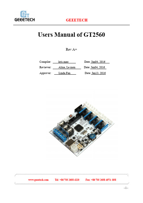
Users Manual of GT2560Rev A+Compiler: kris.mao Date: Jan04, 2016Reviewer: Alina, Le mon Date: Jan04, 2016Approver: Linda.Fan Date: Jan13, 2016 Tel: +86 755 2658 4110 Fax: +86 755 2658 4074 -858ContentsCopyright Declaration (3)Technical Support (3)1 Introduction (4)1.1Overview and Hardware Resources (6)1.2 Software Resources (8)1.3Source (8)2 Interfaces (9)2.1 Interface Layout (9)2.2 Interface specifications (9)2.3 subdivision of stepper motor (10)2.4 Fan connection (11)3 Development Environment setting (13)3.1 Interface Connecting and Setting (13)3.2 Software setting (14)3.3 File Burning (18)4Get Started (21)5 FAQ (25) Tel: +86 755 2658 4110 Fax: +86 755 2658 4074 -858Copyright DeclarationThe copyright of this specification belongs to the Shenzhen GETECH CO., LTD. (hereinafter referred to as the "Geeetech"), and all rights reserved. No part of this specification should be reproduced or extracted in any forms or means without the prior written consent of Geeetech by any company and individuals.Technical SupportIf you are interested in the technology of 3 D printing, flight control and U-home, welcome to Geeetech, we have series of made-up products, main boards, modules and a variety of peripherals for you. Or if you are looking for relevant information or technical support, please login our forum where you can find anything you want about open source. To know more about our new products, please visit , we will serve you wholeheartedly. Tel: +86 755 2658 4110 Fax: +86 755 2658 4074 -8581 IntroductionGT2560 is a compact board that is integrated with the mighty function of the Arduino Mega25 60+Ultimaker and Arduino Mega2560+ramps 1.4 on respect of both software and hardware and has more premium features: the streamlined interfaces effectively avoid the unnecessary troubles, well-regulated compaction of components highly integrated saves more space and easier to be mounted o n most applications.5 stepper motors, swappable driving modules, mighty ATmega2560 processor with 256k mem ory, 16MHz operating frequency, high-performance USB serial converter CH340C, all these make t he GT2560 an ideal option for a 3D printer control board. What’s more, GT2560 can run over 12V t o 24V which gives higher torque and higher rotation rate.Features:1.Integrated with the mighty function of the Arduino Mega2560+Ultimaker and Arduino Mega2560+ramps 1.4 kit, The GT2560 can not only take full place the them on respect of both software and hardware, but also features compact size, more convenient connection, and more stable.2. Adopt ATmega2560 as the main control chip, coupled with the high-performance USB serial converter CH340C.3. The power pack: operating voltage is 12V-24V; double power supply design feeds for heatbed and logical part separately. The current is 15A for heatbed and 10A for other parts.4. The main circuit adopts SMD fuse tube, the diode added to the power port can provide reverse protection to the whole circuit, in addition, the 5V USB is USB port protected with 500mA Recoverable fuse.5.3 12v fan output and one PWM output for LED or other lighting equipment. Tel: +86 755 2658 4110 Fax: +86 755 2658 4074 -8586. 3 55Amp MOSFET (with LED indicator, the actual output is restricted by the PCB board and the connector), all 3 MOSFET are equipped with heat sink to ensure sufficient heat dissipation and stable operation.7. Support 5 A4988 stepper drivers (3 for X/Y/Z axis, and 2 for extruders); the subdivision of stepper motor can be setup by dial switch, eliminating jumper caps, easier to operate.8. 3 temperature sensor input (100k thermistor is recommended)9. Extended LCD and SD card interface support both LCD2004 and LCD 12864, with which you can print without your PC.10. The firmware is the prevalent Marlin, which is known for stability, usability, and high-performance.Update log:1. A 3-pin straight pin is added to connect with 3D touch auto leveling sensor.2. The USB connector will not provide 5V for the board, if you need to refresh the firmware, please provide external power supply.3. The power port has been changed from hollow to solid one to provide higher current-carrying capability.4. The three heater connecter has been changed into blue ones: 2-pin RC3015.0mm 15A Tel: +86 755 2658 4110 Fax: +86 755 2658 4074 -8581.1Overview and Hardware Resources Tel: +86 755 2658 4110 Fax: +86 755 2658 4074 -858 Tel: +86 755 2658 4110 Fax: +86 755 2658 4074 -8581-1(front and back images) Hardware resources 12V/24V 15A and 12V/24V 10A power supply 1 power port for heatbed and 2 for extruder 5 stepper motor input, (3 for X/Y/Z axis, and 2 for extruders) Extended LCD & SD card interface6 endstop input(X-MIN ,Y-MIN ,Z-MIN 和X-MAX ,Y-MAX ,Z-MAX) 3 input for thermistor (TEMP1, TEMP2 and TEMP3)3 input for12V cooling fan1 PWM outputDimension: 109mm*80mm*22mmweight:87 g* The specifications of Pin connectors:Motor: XH (2.54mm-4pin)Fan: PH (2.00mm-3pin)Endstop and thermistor: XH (2.54mm-2pin)1.2 Software ResourcesCompiling environment: Arduino IDEFirmware: Marlin1.3SourceArduino IDE:/wiki/index.php/DownloadMarlin:/wiki/images/3/39/Marlin-Marlin_v1.zipRepetier-Host:/wiki/images/3/36/SetupRepetierHost_1_00.zip Tel: +86 755 2658 4110 Fax: +86 755 2658 4074 -8582 Interfaces2.1 Interface Layout2-12.2 Interface specifications1.DC IN:12V-24V 15A and 12V-24V 10A2. HOT_BED: heat bed3. HEATER1: power supply for extruder 14. HEATER2: power supply for extruder 2 Tel: +86 755 2658 4110 Fax: +86 755 2658 4074 -8585.LCD ENCODER:LCD panel6. SD Card7. X_MIN/X_MAX/Y_MIN /Y_MAX /Z_MIN /Z_MAX: 6 end stop input, XH2.54-2Pin8. TEMP1: temperature sensor for extruder 1, XH2.54-2Pin9. TEMP2: temperature sensor for extruder 2, XH2.54-2Pin10. TEMP3: temperature sensor for heatbed, XH2.54-2Pin11. X,Y,Z:Stepper motors for X, Y, Z axis, XH2.54-4Pin12. EXT1, EXT2(A):Stepper motors for extruder 1 and extruder 2, XH2.54-4Pin13. FAN1,FAN2,FAN3:3 12V cooling fans, PH2.0-3Pin14.1 PWM: PWM output for cooling fan, FAN: PH2.0-3Pin2.3 subdivision of stepper motorUse jumper caps to subdivide stepper motor. When jumper cap is plugged, it is ON.2-21. Subdivision on the base of A4988 stepper driving module: Tel: +86 755 2658 4110 Fax: +86 755 2658 4074 -8582. Subdivision on the base of Drv8825 stepper driving module:2.4 Fan connectionAs default, no matter the power supply is 12V or 24V; you need to connect the 12V fan as ther e is a separate chip that can provide power supply for the fan. If you choose the 24V fan and 24V po wer supply, you need to connect the JP2 with jumper cap. As shown in the picture. Tel: +86 755 2658 4110 Fax: +86 755 2658 4074 -858Note: this function is only available for versions after REV A. Tel: +86 755 2658 4110 Fax: +86 755 2658 4074 -8583 Development Environment setting3.1 Interface Connecting and Setting3-1Note:Pay attention to the Plus-n-Minus of the power connector, reverse connection can cause irrevocably damages. Tel: +86 755 2658 4110 Fax: +86 755 2658 4074 -858A4988 should also be connected to the right port, mismatches and revered directions can cause damage to the main board. You can the correct connections are as follow:3-2If you are using DRV8825 instead of A4988, The correct connections are as follow:3-33.You are suggested to connect all the Periphery modules before testing.3.2 Software settingCH340C Driving Installation:Connect the printer to computer with USB cable. The motherboard driver installer will automatically appear. Please check the following steps.1.When you connect your printer to computer with a USB cable. The following dialog box will Tel: +86 755 2658 4110 Fax: +86 755 2658 4074 -858appear.2.In the Arduino IDE when the CH340C is connected you will see a COM Port in [Devicemanager]. The COM number for your device may vary depending on your system.3.After successful installation, a pop-up box will appear as follows. Tel: +86 755 2658 4110 Fax: +86 755 2658 4074 -858 Tel: +86 755 2658 4110 Fax: +86 755 2658 4074 -858Note: If the driver fails to install automatically, you can finish the installation job manually. Here are the detailed steps.1. Download CH340C here, which is the driver of GT2560:/download/CH341SER_EXE.html (Windows OS) /download/CH341SER_MAC_ZIP.html (MAC OS) /download/CH341SER_LINUX_ZIP.html (LINUX OS) 2. Unzip the file.3. Run the installer which you unzipped.4. In the Arduino IDE when the CH340C is connected you will see a COM Port in [Devicemanager]. The COM number for your device may vary depending on your system. Tel: +86 755 2658 4110 Fax: +86 755 2658 4074 -8585. Click [Install] to continue.6. After successful installation, a pop-up box will appear. Tel: +86 755 2658 4110 Fax: +86 755 2658 4074 -8583.3 File BurningWindows users need install driver before uploading. The board: Tools > Board > Arduino Mega 2560 or Mega ADK, as shown below.3-10Configuring serial interface: Tools > Serial Port > the corresponding COM Port of GT2560 usuallythe last one. As shown below3-11Load in the file you need to burn, Click the “check ()” button to check if it is right and then click the “” button to upload firmware, as shown below. Tel: +86 755 2658 4110 Fax: +86 755 2658 4074 -858 Tel: +86 755 2658 4110 Fax: +86 755 2658 4074 -858图3-123-13Upon uploading, the LED indicator corresponding to the TX , RX and L on the GT2560 will blink, if they stop blinking, it means the file has been uploaded successfully. Tel: +86 755 2658 4110 Fax: +86 755 2658 4074 -8583-14After uploading, you can go on to the next step. If you cannot upload, check the dialog box below to identify the problem and solve it. The common mistakes are the wrong select of type of board or serial port etc.4 Get StartedGT2560 is the CPU of a 3D printer, manipulating the whole process of printing. GT2560 can’t be put in use directly without uploading firmware. 1. Firmware uploading- marlin. 2. Setting parameters of the firmwareThe parameters that need setting are as below, for those not mentioned just leave them as default.#define BAUDRATE 250000This parameter is for the baud rate of serial port. Note: a successful communication can be realizedonly when the Baud rate of upper computer is identical with that of Firmware. The Baud rate is not set in random. The common Baud rate are: 2400,9600,19200,38400,57600,115200,250000. The last three are frequently used for 3D Printer.#define MOTHERBOARD 7This parameter is set for board type. 3D Printer has many types of main board, and the settings of IOs are different, therefore, the parameter has to correspond to the type of your b oard, or it can’t operate normally. The parameter of GT2560 should be 7(single- nozzle). For other board, you can refer to the annotation on the board.#define TEMP_SENSOR_0 1#define TEMP_SENSOR_BED 1The two parameters are set for the type of temperature sensor respectively. They are the critical parameter to check if the sensor read temperature correctly. The printer can’t operate normally, even has potential risk (damage the device and even worse). You must modify depending on the temperature sensor you use.#define EXTRUDE_MINTEMP 170This parameter is set to avoid potential risks when the extruder operates before reaching the rated temperature. If you use other 3D Printer, such as printer to make Chocolates, 45℃is appropriate, so that the parameter configured to a lower value(such as 40℃).const bool X_ENDSTOPS_INVERTING = true; Tel: +86 755 2658 4110 Fax: +86 755 2658 4074 -858const bool Y_ENDSTOPS_INVERTING = true;const bool Z_ENDSTOPS_INVERTING = true.The three parameters are set for the end stops of three axes. If the configuration is true, the end stop outputs 1 in default condition, and outputs 0 when triggered. That is to say, mechanical end stop should connect to the NO (normally open) contactor. If it is connected to the NC (normally closed), true should be changed to false.#define INVERT_X_DIR false#define INVERT_Y_DIR trueMistakes are often made in the above two parameters. The parameters are different for different machinery. In principle, the origin should be at lower-left corner of the print platform (origin: [0, 0]), or at up-right corner (origin: [max, max]). Only in this way will the printing be correct, otherwise, the printing is the mirror image of one axis which is not what expected.#define X_HOME_DIR -1#define Y_HOME_DIR -1#define Z_HOME_DIR -1If the position of the origin is the minimum, the parameter is -1; if it is the maximum, the parameter is 1.#define X_MAX_POS 205#define X_MIN_POS 0#define Y_MAX_POS 205 Tel: +86 755 2658 4110 Fax: +86 755 2658 4074 -858#define Y_MIN_POS 0#define Z_MAX_POS 200#define Z_MIN_POS 0These parameters are crucial to the printing size. Fill in parameters by reference to the coordinate graphs. It is important to note that the origin is not the printing center and the real printing center usually lies at [(x.max - x.min)/2, (y.max -y.min/2)]. The coordinate of central will be used in the slice tool. The printing center’s coordinate must correspond to the parameter configuration, or it will print to the outside of the platform.#define HOMING_FEEDRATE {50*60, 50*60, 4*60, 0}The parameter means the homing speeds (mm/min). This parameter can be set as default if you use the x-axis and y-axis adopt synchronous belt drive and z-axis adopts screw drive.#define DEFAULT_AXIS_STEPS_PER_UNIT {85.3333, 85.3333, 2560, 158.8308}These parameters are crucial to the printing size. These parameters indicate the pulse the axis need when operating 1mm. they are corresponding to x, y, z axis and extruder respectively. In most cases these figure should be calculated by yourself, you can refer to:http://calculator.josefprusa.cz/#steppers.So far, the commonest parameters have been configured and the printer can work now. In addition, if the 2004 LCD needs verifying, you should delete the “//” from “//#define REPRAP_DISCOUNT_SMART_CONTROLLER” to ensure the normal working. Tel: +86 755 2658 4110 Fax: +86 755 2658 4074 -8585 FAQ1. How many extruders can GT2560 support?At most 2 extruders, GT2560 supports 5 A4988 stepper motor drivers, they are X/Y/Z axis and 2 extruders.2. What is the power required?You need to use the 12V-24V power supply, and if you are using the single extruder one, the total power is no less than 200W, if you are using the dual extruder one, the total power is no less than 2 40W.3. The stepper motor on for the extruder doesn’t turn?By default in the firmware, only when the temperature of the extruder reaches 170°C can the moto r turn. Tel: +86 755 2658 4110 Fax: +86 755 2658 4074 -858。
升腾c13参数
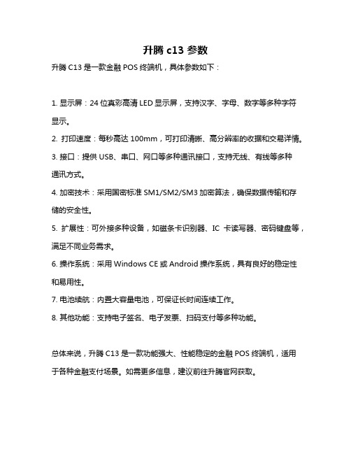
升腾c13参数
升腾C13是一款金融POS终端机,具体参数如下:
1. 显示屏:24位真彩高清LED显示屏,支持汉字、字母、数字等多种字符显示。
2. 打印速度:每秒高达100mm,可打印清晰、高分辨率的收据和交易详情。
3. 接口:提供USB、串口、网口等多种通讯接口,支持无线、有线等多种
通讯方式。
4. 加密技术:采用国密标准SM1/SM2/SM3加密算法,确保数据传输和存储的安全性。
5. 扩展性:可外接多种设备,如磁条卡识别器、IC卡读写器、密码键盘等,满足不同业务需求。
6. 操作系统:采用Windows CE或Android操作系统,具有良好的稳定性和易用性。
7. 电池续航:内置大容量电池,可保证长时间连续工作。
8. 其他功能:支持电子签名、电子发票、扫码支付等多种功能。
总体来说,升腾C13是一款功能强大、性能稳定的金融POS终端机,适用于各种金融支付场景。
如需更多信息,建议前往升腾官网获取。
MAX2605-MAX2609中文资料
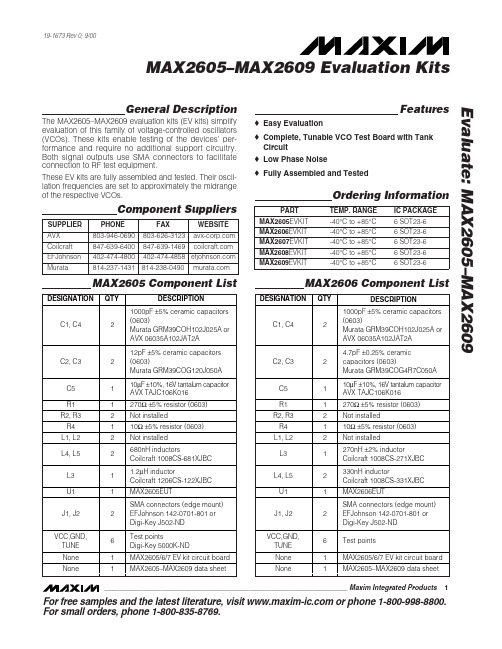
General DescriptionThe MAX2605–MAX2609 evaluation kits (EV kits) simplify evaluation of this family of voltage-controlled oscillators (VCOs). These kits enable testing of the devices’ per-formance and require no additional support circuitry.Both signal outputs use SMA connectors to facilitate connection to RF test equipment.These EV kits are fully assembled and tested. Their oscil-lation frequencies are set to approximately the midrange of the respective VCOs.Featureso Easy Evaluationo Complete, Tunable VCO Test Board with Tank Circuit o Low Phase Noiseo Fully Assembled and TestedEvaluate: MAX2605–MAX2609MAX2605–MAX2609 Evaluation Kits19-1673 Rev 0; 9/00Ordering InformationComponent SuppliersFor free samples and the latest literature, visit or phone 1-800-998-8800.For small orders, phone 1-800-835-8769.MAX2606 Component ListMAX2605 Component ListE v a l u a t e : M A X 2605–M A X 2609MAX2605–MAX2609 Evaluation Kits 2_______________________________________________________________________________________Quick StartThe MAX2605–MAX2609 evaluation kits are fully assembled and factory tested. Follow the instructions in the Connections a nd Setup section for proper device evaluation.Test Equipment Required•Low-noise power supplies (these are recommended for oscillator noise measurement). Noise or ripple will frequency-modulate the oscillator and cause spectral spreading. Batteries can be used in place of power supplies, if necessary.– Use a DC power supply capable of supplying +2.7V to +5.5V. Alternatively, use two or three 1.5V batteries.– Use a DC power supply capable of supplying +0.4V to +2.4V, continuously variable, for TUNE.Alternatively, use two 1.5V batteries with a resistive voltage divider or potentiometer.•An RF spectrum analyzer that covers the operating frequency range of the MAX2605–MAX2609• A 50Ωcoaxial cable with SMA connectors •An ammeter (optional)Connections and Setup1)Connect a DC supply (preset to +3V) to the V CC and GND terminals (through an ammeter, if desired) on the EV kit.2)Turn on the DC supply. If used, the ammeter readingMAX2607 Component ListMAX2608 Component ListEvaluate: MAX2605–MAX2609MAX2605–MAX2609 Evaluation Kits_______________________________________________________________________________________3approximates the typical operating current specified in the MAX2605–MAX2609 data sheet.3)Connect the VCO output (OUT+ or OUT-) to a spec-trum analyzer with a 50Ωcoaxial cable.4)Apply a positive variable DC voltage between 0.4V and 2.4V to TUNE.5)Check the tuning bandwidth on the spectrum analyz-er by varying the tuning voltage (+0.4V to +2.4V).Layout ConsiderationsThe EV kit PC board can serve as a guide for laying out a board using the MAX2605–MAX2609. Generally, the VCC pin on the PC board should have a decoupling capacitor placed close to the IC. This minimizes noisecoupling from the supply. Also, place the VCO as far away as possible from the noisy section of a larger sys-tem, such as a switching regulator or digital circuits.The VCO ’s performance is strongly dependent on the availability of the external tuning inductor. For best per-formance, use high-Q components and choose their val-ues carefully. To minimize the effects of parasitic ele-ments, which degrade circuit performance, place the tuning inductor and C BYP close to the VCO. For higher-frequency versions, include the parasitic PC board inductance and capacitance when calculating the oscillation frequency. In addition, remove the ground plane around and under the tuning inductor to minimize the effect of parasitic capacitance.Noise on TUNE translates into FM noise on the outputs;therefore, keep the trace between TUNE and the control circuitry as short as possible. If necessary, use an RC filter to further suppress noise, as done on the EV kits.E v a l u a t e : M A X 2605–M A X 2609MAX2605–MAX2609 Evaluation Kits 4_______________________________________________________________________________________Figure 2. MAX2608/MAX2609 EV Kits SchematicFigure 1. MAX2605/MAX2606/MAX2607 EV Kits SchematicEvaluate: MAX2605–MAX2609MAX2605–MAX2609 Evaluation Kits_______________________________________________________________________________________5Figure 3. MAX2605/MAX2606/MAX2607 EV Kits ComponentPlacement Guide—Top Silk ScreenFigure 4. MAX2608/MAX2609 EV Kits Component PlacementGuide—Top Silk ScreenFigure 5. MAX2605/MAX2606/MAX2607 EV Kits PC BoardLayout—Component SideFigure 6. MAX2608/MAX2609 EV Kits PC Board Layout—Component SideMa xim ca nnot a ssume responsibility for use of a ny circuitry other tha n circuitry entirely embodied in a Ma xim product. No circuit pa tent licenses a re implied. Maxim reserves the right to change the circuitry and specifications without notice at any time.6_____________________Maxim Integrated Products, 120 San Gabriel Drive, Sunnyvale, CA 94086 408-737-7600©2000 Maxim Integrated ProductsPrinted USAis a registered trademark of Maxim Integrated Products.E v a l u a t e : M A X 2605–M A X 2609MAX2605–MAX2609 Evaluation Kits Figure 7. MAX2605/MAX2606/MAX2607/MAX2608/MAX2609EV Kits PC Board Layout—Ground Plane。
- 1、下载文档前请自行甄别文档内容的完整性,平台不提供额外的编辑、内容补充、找答案等附加服务。
- 2、"仅部分预览"的文档,不可在线预览部分如存在完整性等问题,可反馈申请退款(可完整预览的文档不适用该条件!)。
- 3、如文档侵犯您的权益,请联系客服反馈,我们会尽快为您处理(人工客服工作时间:9:00-18:30)。
元器件交易网
元器件交易网
MAX2650
DC-to-Microwave, +5V Low-Noise Amplifier
______________________________________________________________Pin Description
PIN
NAME
The MAX2650 comes in a 4-pin SOT143 package, requiring minimal board space.
________________________Applications
Wireless Local Loop
Global Positioning Systems (GPS)
2 _______________________________________________________________________________________
元器件交易网
MAX2650
DC-to-Microwave, +5V Low-Noise Amplifier
The device is internally biased, eliminating the need for external bias resistors or inductors. In a typical application, the only external components needed are input and output blocking capacitors and a VCC bypass capacitor.
MAX2650
元器件交易网
19-1135; Rev 1; 8/03 EVAALVUAAILTAIOBNLEKIT
DC-to-Microwave, +5V Low-Noise Amplifier
_______________General Description
The MAX2650 is a low-noise amplifier for use from DC to microwave frequencies. Operating from a single +5V supply, it has a flat gain response to 900MHz. The MAX2650’s low noise figure and high drive capability make it ideal for a variety of transmit, receive, and buffer applications.
SUPPLY CURRENT vs. SUPPLY VOLTAGE
40
OUTPUT 1dB COMPRESSION POINT vs. FREQUENCY
5
OUTPUT 1dB COMPRESSION POINT vs. FREQUENCY
+5
MAX2650-03
MAX2650-02
MAX2650-01
CONDITIONS (Note 1)
fIN = 100MHz to 1000MHz fIN = 800MHz to 1000MHz
Supply Current
TA = TMIN to TMAX VCC = 4.5V to 5.5V
MIN TYP MAX
-40
85
16.5 18.3
21
-1
10
3.9
TOP VIEW
OUT
OUT
CBLOCK
VCC
VCC
CBYP
GND
IN IN
MAX2650
CBLOCK
OUT 3
4 VCC
MAX2650
GND 2
1 IN
SOT143
________________________________________________________________ Maxim Integrated Products 1
1.5:1
1.3:1
300
4.5
5.5
15.5 17.7 20.0
13.0 17.7 22.0
11.0 17.7 24.0
UNITS °C dB dBm dBm dB
ps V
mA
Note 1: Parts are designed to operate over specified temperature range. Specifications are production tested and guaranteed at +25°C.
SOT143-4 (derate 4mW/°C above +70°C)...................320mW
Operating Temperature Range ...........................-40°C to +85°C Junction Temperature ......................................................+150°C Storage Temperature Range .............................-65°C to +150°C Lead Temperature (soldering, 10s) .................................+300°C
MAX2650
DC-to-Microwave, +5V Low-Noise Amplifier
ABSOLUTE MAXIMUM RATINGS
VCC to GND ..............................................................-0.3V to +8V Input Power ....................................................................+13dBm Continuous Power Dissipation (TA = +70°C)
__________________________________________Typical Operating Characteristics
(VCC = 5.0V, Z0 = 50Ω, fIN = 900MHz, TA = +25°C, unless otherwise noted.)
ICC (mA)
30 +85°C
20
10 +25°C
-40°C
0
4.0
4.5
5.0
5.5
6.0
VCC (V)
P-1 (dBm)
3
1 +85°C
-1
-40°C -3
+25°C -5
0.1 0.3 0.5 0.7 0.9 1.1 1.3 1.5 FREQUENCY (GHz)
P-1 (dBm)
+3 5.5V
+1
-1
5.0V
VOLTAGE STANDING-WAVE RATIO vs. FREQUENCY
3.5:1
NOISE FIGURE (dB) MAX2650-07 VSWR MAX2650-06
4
+85°C
+25°C
3
-40°C
3.0:1 2.5:1
2
2.0:1
OUT
1
1.5:1
IN
0 0.1 0.3 0.5 0.7 0.9 1.1 1.3 1.5
4.5V
-3
-5 0.1 0.3 0.5 0.7 0.9 1.1 1.3 1.5
FREQUENCY (GHz)
GAIN (dB) MAX2650-04
GAIN (dB) MAX2650-05
GAIN vs. FREQUENCY
25
+85°C 20
GAIN vs. FREQUENCY
43;25°C -40°C
10
5
15
4.5V 10
5.0V 5
0 0.1 0.3 0.5 0.7 0.9 1.1 1.3 1.5 FREQUENCY (GHz)
NOISE FIGURE vs. FREQUENCY
5
0 0.1 0.3 0.5 0.7 0.9 1.1 1.3 1.5 FREQUENCY (GHz)
______________Ordering Information
PART MAX2650EUS-T
TEMP RANGE -40°C to +85°C
PIN-PACKAGE 4 SOT143-4
__________Typical Operating Circuit
__________________Pin Configuration
FREQUENCY (GHz)
1.0:1 0.1 0.3 0.5 0.7 0.9 1.1 1.3 1.5
FREQUENCY (GHz)
_______________________________________________________________________________________ 3
ISM Radios