MAX5916AUUI+T中文资料
MAX6349VHUT中文资料
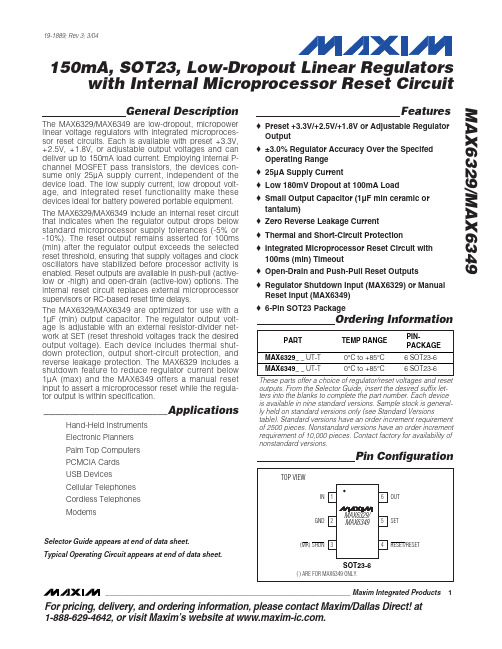
________________________Applications
Hand-Held Instruments
Electronic Planners
Palm Top Computers
PCMCIA Cards
USB Devices
Cellular Telephones
Cordless Telephones
The MAX6329/MAX6349 are optimized for use with a 1µF (min) output capacitor. The regulator output voltage is adjustable with an external resistor-divider network at SET (reset threshold voltages track the desired output voltage). Each device includes thermal shutdown protection, output short-circuit protection, and reverse leakage protection. The MAX6329 includes a shutdown feature to reduce regulator current below 1µA (max) and the MAX6349 offers a manual reset input to assert a microprocessor reset while the regulator output is within specification.
芯片MAX691中文资料

微处理器监控电路MAX691介绍2008年11月07日星期五 22:20max691介绍_微处理器监控电路作者:汪龙景整理:nemoiumMAX691是美国MAXIM公司生产的微处理器监控电路。
由于技术先进,功能完整,精度较高,该电路在自动控制、自动测量及便携产品等领域得到广泛应用。
在法国 THOMCAST公司生和的E—UHF—10003全固态电视发射机中,该芯片应用有六处之多。
现将该集成电路的结构、原理及应用简单介绍如下:一、引脚排列及说明图1所示为MAX691的引脚排列图,分别说明如下:1、VBAn,臼备用电池输入端,连接到外部电池或电容器的充电电路,不用时接地。
2、Vovr一电源电压输出端,不使用备用电池时,可接到Vuo3、Vcc一电源电压输入端。
正常时应为 +5V。
4、GND--~地端5、BATT 0N—电池接通标志端。
当 VouT转接到VBATY时,变为高电平。
6.LOWLINE~电源电压降低标志端。
当 Vcc低于复位门限电压时,LOWLINE 变为低电平。
7、OSC IN—外部振荡器输入端。
8、OSC SEI广振荡器选择端。
9、Pp卜电源故障输入端。
不使用时接地或接Votrro10、PFO一电源故障输出端。
当PFI小于 1.25V时PFO变为低电平。
11、WD卜看门狗输入端。
不使用看门狗功能时悬空。
12、CEOUT—芯片使用输出端13、CEIN—芯片使用输入端。
不使用时接地或接Votrro14、WOD—‘看门狗输出端。
15、RESm,隅复位脉冲输出端,低电平有效。
16、RKSm,畸高电平有效的复位脉冲输出端,该端为漏极开路输出。
一、内部结构及工作原理图2所示为MAX691的内部结构方框图。
由图2知,该集成电路主要由以下几部分组成:1、电源监测及切换电路图2中,两个电压比较器C1、C2,电源切换开关及4.65V的基准电压源等构成电源监测及切换部分。
4。
65V的基准电压源产生复位门限电平,Ve与它在C:中进行比较。
5916中文资料
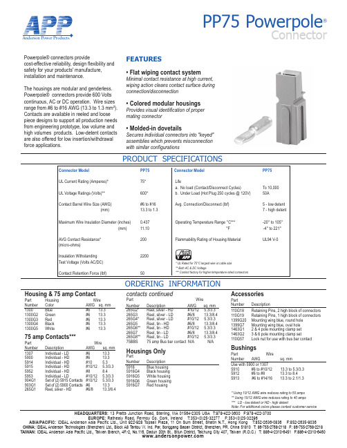
Anderson Power Products®HEADQUARTERS: 13 Pratts Junction Road, Sterling, MA 01564-2305 USA T:978-422-3600 F:978-422-3700EUROPE: Rathealy Road, Fermoy Co. Cork, Ireland T:353-(0)25-32277 F:353-(0)25-32296ASIA/PACIFIC: IDEAL Anderson Asia Pacific Ltd., Unit 922-928 Topsail Plaza, 11 On Sum Street, Shatin N.T., Hong Kong T:852-2636-0836 F:852-2635-9036CHINA: IDEAL Anderson T echnologies (Shenzhen) Ltd., Block A8 T antou W. Ind. Par, Songgang Baoan District, Shenzhen, PR. China 51810 T: 86-755-2768-2118 F: 86-755-2768-2218TAIWAN: IDEAL Anderson Asia Pacific Ltd., Taiwan Branch, 4F.-2, No.116, Dadun 20th St., Situn District, Taichung City 407, Taiwan (R.O.C.) T: 886-4-2310-6451 F:886-4-2310-6460PP75 Powerpole®ConnectorORDERING INFORMATIONAccessoriesPartNumber Description110G18 Retaining Pins, 2 high block of connectors 110G19 Retaining Pins, 1 high block of connectors 1399G20 Mounting wing blue, round hole 1399G7 Mounting wing blue, oval hole 1463G1 2 & 4 pole mounting clamp set 1463G2 3 & 6 pole mounting clamp set110G57 Lock nut for use with bus bar contactBushingsPart WireNumber AWG sq. mm 5910 #6 to #10/12 13.3 to 5.3/3.35912 #6 to #8 13.3 to 8.45913 #6 to #14/16 13.3 to 2.1/1.3Powerpole® connectors providecost-effective reliability, design flexibility and safety for your products' manufacture, installation and maintenance.The housings are modular and genderless. Powerpole® connectors provide 600 Volts continuous, AC or DC operation. Wire sizes range from #6 to #16 AWG (13.3 to 1.3 mm²). Contacts are available in reeled and loose piece designs to support all production needs from engineering prototype, low volume and high volumes products. Low-detent contacts are also offered for low insertion/withdrawal force applications.Housing & 75 amp ContactPart Housing WireNumber Color AWG sq. mm 1300 Blue #6 13.31300G2 Green #6 13.31300G3 Red #6 13.31300G4 Black #6 13.31300G5 White#6 13.375 amp Contacts***Part WireNumber Description AWG sq. mm 1307 Individual - LD #6 13.35900 Individual - HD #6 13.35914 Individual - HD #10 5.35915 Individual - HD #10/12 5.3/3.35952 Individual - HD #8 8.45953 Individual - LD#10/12 5.3/3.3904G1 Set of (2) 5915 Contacts #10/12 5.3/3.3903G1 Set of (2) 5900 Contacts #6 13.3265G1Reel, silver - HD #6/8 13.3/8.4contacts continuedPartWire Number Description AWG sq. mm 265G2* Reel, silver - HD #10/12 5.3/3.3265G3 Reel, silver - LD #6/8 13.3/8.4265G4* Reel, silver - LD #10/12 5.3/3.3265G5 Reel, tin - HD #6/8 13.3/8.4265G6** Reel, tin - HD #10/12 5.3/3.3265G7 Reel, tin - LD #6/8 13.3/8.4265G8** Reel, tin - LD #10/12 5.3/3.375BBS75 amp Bus bar contact N/A N/AHousings OnlyPartNumber Description 15916G4 Black housing 5916G5 White housing 5916G6 Green housing 5916G7 Red housingFEATURES• Flat wiping contact systemMinimal contact resistance at high current, wiping action cleans contact surface during connection/disconnection • Colored modular housingsProvides visual identification of proper mating connector• Molded-in dovetailsSecures individual connectors into "keyed" assemblies which prevents misconnection with similar configurations* Using 10/12 AWG wire reduces rating to 50 amps ** Using 10/12 AWG wire reduces rating to 40 amps *** LD - low detent or HD - high detentNote: For additional colors please contact customer serviceAnderson Power Products®HEADQUARTERS: 13 Pratts Junction Road, Sterling, MA 01564-2305 USA T:978-422-3600 F:978-422-3700EUROPE: Rathealy Road, Fermoy Co. Cork, Ireland T:353-(0)25-32277 F:353-(0)25-32296ASIA/PACIFIC: IDEAL Anderson Asia Pacific Ltd., Unit 922-928 Topsail Plaza, 11 On Sum Street, Shatin N.T., Hong Kong T:852-2636-0836 F:852-2635-9036CHINA: IDEAL Anderson Technologies (Shenzhen) Ltd., Block A8 T antou W. Ind. Par, Songgang Baoan District, Shenzhen, PR. China 51810 T : 86-755-2768-2118 F: 86-755-2768-2218TAIWAN: IDEAL Anderson Asia Pacific Ltd., Taiwan Branch, 4F.-2, No.116, Dadun 20th St., Situn District, Taichung City 407, Taiwan (R.O.C.) T: 886-4-2310-6451 F:886-4-2310-6460PP75 Powerpole ®ConnectorDIMENSIONSToolingPartNumber Description1309G4 Hand tool, #16 to #61387G1 Pneumatic tool, #16 to #61388G6 - die for #16 to #6 AWG1388G7 - die for #10 to #12 AWG (5914, 5915 & 5953 contacts)1389G6 - locator for #16 to #6 AWG1389G7 - locator for #10 to #12 AWG (5914, 5915 & 5953 contacts)260G16Applicator only (110V & 220V)284G1 Applicator & Press (220V, 50Hz)250G5 Press only (110V, 60Hz)2 or 4 Pole PoleORDERING INFORMATIONTEMPERATURE RISE CHARTS1463G1 41.1 1.62 50.7 2.00 43.1 1.70 31.8 1.25 4.0 0.16 (4 Pole)1463G2 57.2 2.25 34.7 1.37 27.1 1.07 47.6 1.88 4.0 0.16 (3 Pole)1463G2 57.2 2.2550.7 2.00 43.1 1.70 47.6 1.88 4.0 0.16 (6 Pole)ContactsPart -A- -B- -C- -D- -E- -F- 01020304050607080900102030405060708090PP75 (Reeled Contacts) Multipole - Silver PlatedTemperature Rise at Constant CurrentAmperes AppliedT e m p e r a t u r e (°C )01020304050607080900102030405060708090PP75 (Reeled Contacts) Multipole - Tin PlatedTemperature Rise at Constant CurrentT e m p e r a t u r e (°C )010203040PP75 SinglepoleAmperes AppliedT e m p e r a t u r e (°C )PP75 MultipoleAmperes AppliedT e m p e r a t u r e (°C )10203040Duration of Current (seconds)Am p e r e s204060801001201401601802002202402602800.51248163264128256PP75 Multipole Pulse Current CapabilityAmperes Applied6 AWG 8 AWG 10 AWG 12 AWG6 AWG 8 AWG 10 AWG 12 AWG6 AWG 8 AWG 10 AWG 12 AWG6 AWG 8 AWG 10 AWG 12 AWG6 AWG 8 AWG 10 AWG 12 AWGHousing[ 15.9 ]All Data Subject To Change Without NoticeDS-PP75 REV04。
MAX5915A中文资料

MAX706中文资料_数据手册_参数

UNREGULATED DC
MAX667 +5V DC LINEAR
REGULATOR
PUSHBUTTON SWITCH
VCC
RESMR
MAX706 MAX813L
PFO
µP
VCC RESET I/O LINE NMI INTERRUPT
___________________________Features
o Available in Tiny µMAX Package
o Guaranteed RESET Valid at VCC = 1V o Precision Supply-Voltage Monitor
4.65V in MAX705/MAX707/MAX813L 4.40V in MAX706/MAX708
Output Current (all outputs) . . . . . . . . . . . . . . . . . . . . . . . . . . . . . 20mA Continuous Power Dissipation (TA = +70°C)
Plastic DIP (derate 9.09mW/°C above +70°C) . . . . . . . 727mW SO (derate 5.88mW/°C above +70°C) . . . . . . . . . . . . . . . 471mW µMAX (derate 4.10mW/°C above +70°C) . . . . . . . . . . . . 330mW
3) A 1.25V threshold detector for power-fail warning, low-battery detection, or for monitoring a power supply other than +5V.
MAX1615中文资料
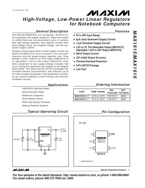
(VIN = 15V, SHDN = VIN, ILOAD = 5µA, TA = TMIN to TMAX, unless otherwise noted. Typical values are at TA = +25°C.) (Note 2) PARAMETER Input Voltage Range Supply Current Minimum Load Current Shutdown Supply Current Dropout Supply Current IIN SHDN = GND (shutdown mode) Output set to 5V, VIN = 4V ILOAD = 1mA, TA = +25°C, VIN = 6V to 28V ILOAD = 5µA to 30mA, TA = TMIN to TMAX, VIN = 6V to 28V FB = OUT, VIN = 6V to 28V VFB = 1.3V ILOAD = 30mA (Note 4) VIN = 6V IN = unconnected, VOUT forced to 5V MAX1615 MAX1616 Rising edge of IN or SHDN to OUT within specification limits, RL = 500Ω, COUT = 6.8µF, VOUT set to 5V VOSH RL = 500Ω, COUT = 10µF within 90% of nominal output voltage 0.5 0.16 0.23 1 100 70 TA = +25°C TMIN = TMIN to TMAX TA = +25°C 5/3 = GND 5/3 = OUT 5/3 = GND 5/3 = OUT TA = +25°C, ILOAD = 1mA TA = TMIN to TMAX, ILOAD = 5µA to 30mA 3.26 4.95 3.15 4.75 1.215 1.18 -10 12 1.240 70 3.33 5.05 3.40 5.15 V 3.48 5.25 1.265 1.28 30 350 V V nA mV mA µA µF/mA SYMBOL VIN IIN SHDN = IN, TA = +25°C SHDN = IN, VIN = 6V to 28V, TA = TMIN to TMAX CONDITIONS MIN 4 6.2 TYP MAX 28 8 15 5 1.5 3 UNITS V µA µA µA µA
MAX2605-MAX2609中文资料
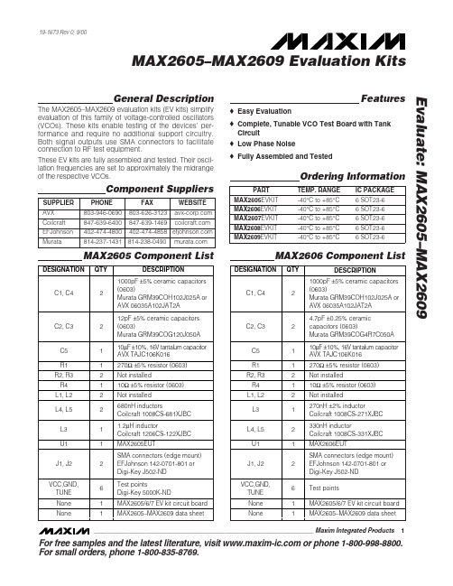
General DescriptionThe MAX2605–MAX2609 evaluation kits (EV kits) simplify evaluation of this family of voltage-controlled oscillators (VCOs). These kits enable testing of the devices’ per-formance and require no additional support circuitry.Both signal outputs use SMA connectors to facilitate connection to RF test equipment.These EV kits are fully assembled and tested. Their oscil-lation frequencies are set to approximately the midrange of the respective VCOs.Featureso Easy Evaluationo Complete, Tunable VCO Test Board with Tank Circuit o Low Phase Noiseo Fully Assembled and TestedEvaluate: MAX2605–MAX2609MAX2605–MAX2609 Evaluation Kits19-1673 Rev 0; 9/00Ordering InformationComponent SuppliersFor free samples and the latest literature, visit or phone 1-800-998-8800.For small orders, phone 1-800-835-8769.MAX2606 Component ListMAX2605 Component ListE v a l u a t e : M A X 2605–M A X 2609MAX2605–MAX2609 Evaluation Kits 2_______________________________________________________________________________________Quick StartThe MAX2605–MAX2609 evaluation kits are fully assembled and factory tested. Follow the instructions in the Connections a nd Setup section for proper device evaluation.Test Equipment Required•Low-noise power supplies (these are recommended for oscillator noise measurement). Noise or ripple will frequency-modulate the oscillator and cause spectral spreading. Batteries can be used in place of power supplies, if necessary.– Use a DC power supply capable of supplying +2.7V to +5.5V. Alternatively, use two or three 1.5V batteries.– Use a DC power supply capable of supplying +0.4V to +2.4V, continuously variable, for TUNE.Alternatively, use two 1.5V batteries with a resistive voltage divider or potentiometer.•An RF spectrum analyzer that covers the operating frequency range of the MAX2605–MAX2609• A 50Ωcoaxial cable with SMA connectors •An ammeter (optional)Connections and Setup1)Connect a DC supply (preset to +3V) to the V CC and GND terminals (through an ammeter, if desired) on the EV kit.2)Turn on the DC supply. If used, the ammeter readingMAX2607 Component ListMAX2608 Component ListEvaluate: MAX2605–MAX2609MAX2605–MAX2609 Evaluation Kits_______________________________________________________________________________________3approximates the typical operating current specified in the MAX2605–MAX2609 data sheet.3)Connect the VCO output (OUT+ or OUT-) to a spec-trum analyzer with a 50Ωcoaxial cable.4)Apply a positive variable DC voltage between 0.4V and 2.4V to TUNE.5)Check the tuning bandwidth on the spectrum analyz-er by varying the tuning voltage (+0.4V to +2.4V).Layout ConsiderationsThe EV kit PC board can serve as a guide for laying out a board using the MAX2605–MAX2609. Generally, the VCC pin on the PC board should have a decoupling capacitor placed close to the IC. This minimizes noisecoupling from the supply. Also, place the VCO as far away as possible from the noisy section of a larger sys-tem, such as a switching regulator or digital circuits.The VCO ’s performance is strongly dependent on the availability of the external tuning inductor. For best per-formance, use high-Q components and choose their val-ues carefully. To minimize the effects of parasitic ele-ments, which degrade circuit performance, place the tuning inductor and C BYP close to the VCO. For higher-frequency versions, include the parasitic PC board inductance and capacitance when calculating the oscillation frequency. In addition, remove the ground plane around and under the tuning inductor to minimize the effect of parasitic capacitance.Noise on TUNE translates into FM noise on the outputs;therefore, keep the trace between TUNE and the control circuitry as short as possible. If necessary, use an RC filter to further suppress noise, as done on the EV kits.E v a l u a t e : M A X 2605–M A X 2609MAX2605–MAX2609 Evaluation Kits 4_______________________________________________________________________________________Figure 2. MAX2608/MAX2609 EV Kits SchematicFigure 1. MAX2605/MAX2606/MAX2607 EV Kits SchematicEvaluate: MAX2605–MAX2609MAX2605–MAX2609 Evaluation Kits_______________________________________________________________________________________5Figure 3. MAX2605/MAX2606/MAX2607 EV Kits ComponentPlacement Guide—Top Silk ScreenFigure 4. MAX2608/MAX2609 EV Kits Component PlacementGuide—Top Silk ScreenFigure 5. MAX2605/MAX2606/MAX2607 EV Kits PC BoardLayout—Component SideFigure 6. MAX2608/MAX2609 EV Kits PC Board Layout—Component SideMa xim ca nnot a ssume responsibility for use of a ny circuitry other tha n circuitry entirely embodied in a Ma xim product. No circuit pa tent licenses a re implied. Maxim reserves the right to change the circuitry and specifications without notice at any time.6_____________________Maxim Integrated Products, 120 San Gabriel Drive, Sunnyvale, CA 94086 408-737-7600©2000 Maxim Integrated ProductsPrinted USAis a registered trademark of Maxim Integrated Products.E v a l u a t e : M A X 2605–M A X 2609MAX2605–MAX2609 Evaluation Kits Figure 7. MAX2605/MAX2606/MAX2607/MAX2608/MAX2609EV Kits PC Board Layout—Ground Plane。
MB90591GPF中文资料

3
元器件交易网
MB90590/590G Series
s PRODUCT LINEUP
Features Classification ROM size RAM size Emulator-specific power supply *1 MB90591/591G/594/594G Mask ROM product 384/256 Kbytes 8/6 Kbytes MB90F591A/F591G/ F594A/F594G Flash ROM product 384/256 Kbytes Boot block Hard-wired reset vector 8/6 Kbytes MB90V590A/V590G Evaluation product None 8 Kbytes None
2
元器件交易网
MB90590/590G Series
• 16-bit I/O timer 16-bit free-run timer : 1 channel Input capture : 6 channels Output compare : 6 channels • Extended I/O serial interface : 1 channel • UART (3 channels) With full-duplex double buffer (8-bit length) Clock asynchronized or clock synchronized (with start/stop bit) transmission can be selectively used. • Stepping motor controller (4 channels) • External interrupt circuit (8 channels) A module for starting an extended intelligent I/O service (EI2OS) and generating an external interrupt which is triggered by an external input. • Delayed interrupt generation module Generates an interrupt request for switching tasks. • 8/10-bit A/D converter (8 channels) 8/10-bit resolution can be selectively used. Starting by an external trigger input. • FULL-CAN interfaces : 2 Conforming to Version 2.0 Part A and Part B Flexible message buffering (mailbox and FIFO buffering can be mixed) • Sound generator • 18-bit Time-base counter • Clock timer : 1 channel • External bus interface : Maximum address space 16 Mbytes * : Embedded Algorithm is a trade mark of Advanced Micro Devi MB90590/590G series with two FULL-CAN*1 interfaces and FLASH ROM is especially designed for automotive and industrial applications. Its main features are two on board CAN Interfaces, which conform to V2.0 Part A and Part B, while supporting a very flexible message buffer scheme and so offering more functions than a normal full CAN approach. The instruction set of F2MC-16LX CPU core inherits an AT architecture of the F2MC*2 family with additional instruction sets for high-level languages, extended addressing mode, enhanced multiplication/division instructions, and enhanced bit manipulation instructions. The microcontroller has a 32-bit accumulator for processing long word data. The MB90590/590G series has peripheral resources of 8/10-bit A/D converters, UART (SCI), extended I/O serial interface, 8/16-bit PPG timer, I/O timer (input capture (ICU), output compare (OCU)), stepping motor controller, and sound generator. *1 : Controller Area Network (CAN) - License of Robert Bosch GmbH *2 : F2MC stands for FUJITSU Flexible Microcontroller.
- 1、下载文档前请自行甄别文档内容的完整性,平台不提供额外的编辑、内容补充、找答案等附加服务。
- 2、"仅部分预览"的文档,不可在线预览部分如存在完整性等问题,可反馈申请退款(可完整预览的文档不适用该条件!)。
- 3、如文档侵犯您的权益,请联系客服反馈,我们会尽快为您处理(人工客服工作时间:9:00-18:30)。
General DescriptionThe MAX5915/MAX5915A/MAX5916/MAX5916A dual PCI 2.2 hot-swap controllers allow for safe insertion and removal of two PCI cards into live PCI slots or back-planes by limiting the inrush current at startup. After startup, these devices provide protection against short-circuit, overcurrent, and undervoltage conditions.The MAX5915/MAX5915A/MAX5916/MAX5916A pro-vide independent power controls for +3.3V, +5V, ±12V,and +3.3V auxiliary supplies of two PCI cards. These devices provide intelligent selective thermal shutdown control that shuts down the channel with an overcurrent fault. All devices include internal power MOSFETs for the +12V, -12V, and +3.3V auxiliary outputs. These devices use internal charge pumps to activate the gates of the internal FETs controlling the +3.3V auxiliary supply.Internal FETs and current-sense circuitry regulate the ±12V and the +3.3V auxiliary supplies. Channels A and B operate independently, allowing a single device to moni-tor two PCI card slots.The MAX5915/MAX5915A offer latched fault protection and the MAX5916/MAX5916A offer autorestart fault pro-tection. The devices are available in the low-profile 28-pin TSSOP package.Features♦PCI 2.2 Compliant♦Independent Power Controls for +3.3V, +5V, ±12V,and +3.3V Auxiliary Supplies of Two PCI Cards ♦Internal MOSFET Switches for ±12V and +3.3V Auxiliary Outputs ♦Separate ON/OFF Control Input for Each Channel ♦Independent +3.3V Auxiliary Output ON/OFF Control ♦Overcurrent Foldback with Timeout and Shutdown Protection for ±12V and +3.3V Auxiliary Rails with Status Report ♦Brick Wall with Timeout and Shutdown Protection for +5V and +3.3V Rails with Status Report ♦Output Undervoltage Monitoring for +3.3V, +5V,+12V, and +3.3V Auxiliary Rails with Status Report ♦+3.3V Auxiliary Autorestart♦Intelligent Selective Thermal Shutdown Control Shuts Down Only the Channel with an Overcurrent Fault ♦28-Pin TSSOP PackageMAX5915/MAX5915A/MAX5916/MAX5916ADual PCI 2.2 Hot-Swap Controllers________________________________________________________________Maxim Integrated Products 119-2420; Rev 2; 9/05For pricing, delivery, and ordering information,please contact Maxim/Dallas Direct!at 1-888-629-4642, or visit Maxim’s website at .Ordering InformationApplicationsPCI 2.2 Server PCI Server RAIDSelector Guide, Pin Configuration, Functional Diagram, and Typical Operating Circuit appear at end of data sheet.Typical Application Circuit*Contact factory for availabilty.M A X 5915/M A X 5915A /M A X 5916/M A X 5916ADual PCI 2.2 Hot-Swap Controllers 2_______________________________________________________________________________________ABSOLUTE MAXIMUM RATINGSStresses beyond those listed under “Absolute Maximum Ratings” may cause permanent damage to the device. These are stress ratings only, and functional operation of the device at these or any other conditions beyond those indicated in the operational sections of the specifications is not implied. Exposure to absolute maximum rating conditions for extended periods may affect device reliability.+12VIN to GND ...................................................-0.3V to +14.0V -12VIN to GND........................................................-14V to +0.3V -12VO_ to GND......................................+0.3V to (V -12VIN - 0.3V)+12VO_, 3.3VGATE_, 5VGATE_to GND..................................................-0.3V to (V +12VIN + 0.3V)Any Other Pin to GND ...........................................-0.3V to +6.0V Continuous Power Dissipation (T A = +70°C)28-Pin TSSOP (derate 23.8mW/°C above +70°C)...........1.9WOperating Temperature Ranges:MAX591_U_ _......................................................0°C to +85°C MAX591_A U_ _...................................................0°C to +85°C MAX591_E_ _....................................................-40°C to +85°C MAX591_ AE_ _................................................-40°C to +85°C Maximum Junction Temperature.....................................+150°C Storage Temperature Range.............................-65°C to +150°C Lead Temperature (soldering, 10s).................................+300°CELECTRICAL CHARACTERISTICSELECTRICAL CHARACTERISTICS (continued)MAX5915/MAX5915A/MAX5916/MAX5916A Dual PCI 2.2 Hot-Swap ControllersM A X 5915/M A X 5915A /M A X 5916/M A X 5916ADual PCI 2.2 Hot-Swap Controllers 4_______________________________________________________________________________________ELECTRICAL CHARACTERISTICS (continued)Note 3:t DEG is negative edge triggered. ON_ or AUXON_ transition from low to high has no delay.Note 4:Temperature threshold at which the outputs of the channel with overcurrent shut down.Note 5:The temperature threshold at which both channels shut down.MAX5915/MAX5915A/MAX5916/MAX5916ADual PCI 2.2 Hot-Swap Controllers_______________________________________________________________________________________5Typical Operating Characteristics(V +12VIN = +12V, V 3.3VAUXIN = +3.3V, V -12VIN = -12V, V 5V = +5V, V 3.3V = +3.3V, R 5VSEN_= 0.005Ω, R 3.3VSEN_ = 0.005Ω, C 3.3VO_ =M A X 5915 t o c 09OUTPUT CURRENT (A)3.3V A U X _ V O L T A G E (V )1.050.900.600.750.300.450.152.62.72.82.93.03.13.23.33.43.52.50 1.203.3VAUX_ VOLTAGE vs. OUTPUT CURRENT3.3VO_ SENSE RESISTOR VOLTAGE vs. DIFFERENTIAL SWITCH VOLTAGEV IN - V3.3VSEN_ (V)3.3V O _ C U R R E N T -L I M I T T H R E S H O L D (m V )30343236384246444840 3.02.51.52.01.03.53.3VO_ VOLTAGE vs. OUTPUT CURRENTOUTPUT CURRENT (A)3.3V O _ V O L T A G E (V )23.183.203.223.283.303.323.168463.243.26202422282630343836401.01.52.02.53.03.54.04.55.05VO_ SENSE RESISTOR VOLTAGE vs. DIFFERENTIAL SWITCH VOLTAGEV IN - V 5VSEN_ (V)5V O _ C U R R E N T -L I M I T T H R E S H O L D (m V )325VO_ VOLTAGE vs. OUTPUT CURRENTOUTPUT CURRENT (A)5V O _ V O L T A G E (V )14.824.844.864.884.904.924.8052344.944.964.985.005.02-12VO_ CURRENT FOLDBACK vs. DIFFERENTIAL SWITCH VOLTAGEM A X 5915 t o c 04V -12VIN - V -12VO_ (V)-12V O _ C U R R E N T F O L D B A C K (m A )250100150200250004681012-12VO_ VOLTAGE vs. OUTPUT CURRENTM A X 5915 t o c 03OUTPUT CURRENT (mA)-12V O _ V O L T A G E (V )50-12.0-11.9-11.8-11.7-11.6-11.5-12.10250100150200+12VO_ CURRENT FOLDBACK vs. DIFFERENTIAL SWITCH VOLTAGEM A X 5915 t o c 02V +12VIN - V +12VO_ (V)+12V O _ C U R R E N T F O L D B A C K (A )20.10.30.50.70.91.1-0.104681012+12VO_ VOLTAGE vs. OUTPUT CURRENTM A X 5915 t o c 01OUTPUT CURRENT (A)+12V O _ V O L T A G E (V )1.00.511.511.611.711.811.912.012.111.41.5M A X 5915/M A X 5915A /M A X 5916/M A X 5916ADual PCI 2.2 Hot-Swap Controllers 6_______________________________________________________________________________________Typical Operating Characteristics (continued)(V +12VIN = +12V, V 3.3VAUXIN = +3.3V, V -12VIN = -12V, V 5V = +5V, V 3.3V = +3.3V, R 5VSEN_= 0.005Ω, R 3.3VSEN_ = 0.005Ω, C 3.3VO_ =2ms/divTIME-TO-CHARGE GATE(C GATE = 10nF)ON_5V/div3.3VGATE_5V/div MAX5915 toc185VGATE_ 5V/div200µs/divTIME-TO-CHARGE GATE(C GATE = 1nF)ON_5V/div 3.3VGATE_5V/div MAX5915 toc175VGATE_5V/div100µs/divTIME-TO-CHARGE GATE(C GATE = 0.1nF)ON_5V/div 3.3VGATE_5V/div MAX5915 toc165VGATE_5V/divM A X 5915 t o c 15TEMPERATURE (°C)-12V I N T E R N A L S W I T C H R O N (Ω)6035-15100.10.20.30.40.50.60.70.80-4085-12V INTERNAL SWITCH R ONvs. TEMPERATUREM A X 5915 t o c 14TEMPERATURE (°C)3.3V A U X I L I A R Y I N T E R N A L S W I T C H R O N (Ω)603510-150.050.100.150.200.250.300.350-40853.3V AUXILIARY INTERNAL SWITCH R ONvs. TEMPERATUREM A X 515 t o c 13TEMPERATURE (°C)+12V I N T E R N A L S W I T C H R O N (Ω)603510-150.050.100.150.200.250.300.350.400.450-4085+12V INTERNAL SWITCH R ONvs. TEMPERATURE5VGATE_ AND 3.3VGATE_DISCHARGE CURRENT vs. TEMPERATURETEMPERATURE (°C)G A T E D I S C H A R G E C U R R E N T (µA )603510-15135140145150155160165170175180130-40855VGATE_ AND 3.3VGATE_CHARGE CURRENT vs. TEMPERATURETEMPERATURE (°C)G A T E C H A R G E C U R R E N T (µA )603510-159.511.513.515.517.519.521.523.525.527.57.5-40853.3VAUX_ CURRENT FOLDBACK vs. DIFFERENTIAL SWITCH VOLTAGEM A X 5915 t o c 10V 3.3VAUXIN - V 3.3VAUXO_ (V)3.3V A U X _ C U R R E N T F O L D B A C K (m A )0.55506006507007508005001.02.02.53.01.53.5MAX5915/MAX5915A/MAX5916/MAX5916ADual PCI 2.2 Hot-Swap Controllers_______________________________________________________________________________________7Typical Operating Characteristics (continued)(V +12VIN = +12V, V 3.3VAUXIN = +3.3V, V -12VIN = -12V, V 5V = +5V, V 3.3V = +3.3V, R 5VSEN_= 0.005Ω, R 3.3VSEN_ = 0.005Ω, C 3.3VO_ =M A X 5915 t o c 27TEMPERATURE (°C)+12V I N P U T U V L O T H R E S H O L D (V )603510-159.69.79.89.910.010.110.210.310.410.59.5-4085+12V INPUT UVLOTHRESHOLD vs. TEMPERATURE3.3V AUXILIARY INPUT UVLO THRESHOLD vs. TEMPERATUREM A X 5915 t o c 26TEMPERATURE (°C)3.3V A U X I L I A R Y I N P U T U V L O T H R E S H O L D (V )6035-15102.62.72.82.93.03.13.23.32.5-40853.3V AUXILIARY OUTPUT UNDERVOLTAGETHRESHOLD vs. TEMPERATUREM A X 5915 t o c 25TEMPERATURE (°C)3.3V A U X I L I A R Y O U T P U T U N D E R V O L T A G E T H R E S H O L D (V )603510-152.82.93.03.13.23.32.7-4085 3.3V OUTPUT UNDERVOLTAGE THRESHOLD vs. TEMPERATUREM A X 5915 t o c 24TEMPERATURE (°C)3.3V O U T P U T U N D E R V O L T A G E T H R E S H O L D (V )6035-15102.62.72.82.93.03.13.23.32.5-40855V OUTPUT UNDERVOLTAGE THRESHOLD vs. TEMPERATUREM A X 5915 t o c 23TEMPERATURE (°C)5V O U T P U T U N D E R V O L T A G E T H R E S H O L D (V )603510-154.434.484.534.584.634.684.38-4085+12V OUTPUT UNDERVOLTAGE THRESHOLD vs. TEMPERATUREM A X 5915 t o c 22TEMPERATURE (°C)+12V O U T P U T U N D E R V O L T A G E T H R E S H O L D (V )603510-1510.310.410.510.610.710.810.2-4085ON_ AND AUXON_ THRESHOLDvs. TEMPERATUREM A X 5915 t o c 21TEMPERATURE (°C)O N _ A N D A U X O N _ T H R E S H O L D (V )603510-151.851.901.952.00RISINGFALLING2.052.101.80-40853.3VAUXIN SUPPLY CURRENTvs. TEMPERATUREM A X 5915 t o c 20TEMPERATURE (°C)3.3V A U X I N S U P P L Y C U R R E N T (m A )603510-150.250.500.751.001.251.501.752.002.252.500-4085+12VIN SUPPLY CURRENT vs. TEMPERATUREM A X 5915 t o c 19TEMPERATURE (°C)+12V I N S U P P L Y C U R R E N T (m A )603510-152.12.22.32.42.52.62.72.82.93.02.0-4085M A X 5915/M A X 5915A /M A X 5916/M A X 5916ADual PCI 2.2 Hot-Swap Controllers 8_______________________________________________________________________________________Typical Operating Characteristics (continued)(V +12VIN = +12V, V 3.3VAUXIN = +3.3V, V -12VIN = -12V, V 5V = +5V, V 3.3V = +3.3V, R 5VSEN_= 0.005Ω, R 3.3VSEN_ = 0.005Ω, C 3.3VO_ =40ms/divMAIN SUPPLY TURN-OFF WAVEFORMSON_ 5V/div +12VO_10V/divMAX5915 toc36PGOOD_5V/div5VO_ 5V/div 200µs/divTURN-ON DELAY+12VIN 10V/div 3.3VAUXIN_2V/div3.3VAUXO_2V/div+12VO_10V/div ON_ = 5V AUXON_ = 5V10ms/divAUXILIARY SUPPLY TURN-ON WAVEFORMSAUXON_5V/div3.3VAUXO_2V/divPGOOD_ 5V/divON_ = 5.0V10ms/divMAIN SUPPLY TURN-ON WAVEFORMSON_ 5V/div12VO_ 10V/div PGOOD_ 5V/div5VO_ 5V/div AUXON_ = 5V5VO_ SENSE RESISTOR VOLTAGEvs. TEMPERATURETEMPERATURE (°C)5V 0_ S E N S E R E S I S T O R V O L T A G E (m V )6035-1510242220262834363840-408532303.3V AUXILIARY CURRENT FOLDBACK vs. TEMPERATUREM A X 5915 t o c 31TEMPERATURE (°C)3.3V A X I L I A R Y C U R R E N T F O L D B A C K (m A )6035-1510475550625700775850925-40853.3VO_ SENSE RESISTOR VOLTAGEvs. TEMPERATURETEMPERATURE (°C)3.3V S E N S E R E S I S T O R V O L T A G E (m V )603510-15373941434535-40854749-12V OUTPUT CURRENT FOLDBACK vs. TEMPERATUREM A X 5915 t o c 29TEMPERATURE (°C)-12V O U T P U T C U R R E N T F O L D B A C K (m A )6035-1510130150170************-4085M A X 5915 t o c 28TEMPERATURE (°C)+12V O U T P U T C U R R E N T F O L D B A C K (A )603510-150.70.80.91.01.11.20.6-4085+12V OUTPUT CURRENT FOLDBACK vs. TEMPERATUREMAX5915/MAX5915A/MAX5916/MAX5916ADual PCI 2.2 Hot-Swap Controllers_______________________________________________________________________________________9Typical Operating Characteristics (continued)(V +12VIN = +12V, V 3.3VAUXIN = +3.3V, V -12VIN = -12V, V 5V = +5V, V 3.3V = +3.3V, R 5VSEN_= 0.005Ω, R 3.3VSEN_ = 0.005Ω, C 3.3VO_=-12VO_ CURRENT FOLDBACKMAX5915 toc452ms/divI -12VO_500mA/divPGOOD_5V/div-12VO_5V/div-12VO_ IMMEDIATE SHORT-CIRCUIT RESPONSEMAX5915 toc44200ns/divI -12VO_2A/divPGOOD_5V/div-12VO_5V/div+12VO_ CURRENT FOLDBACKMAX5915 toc432ms/divI +12VO_5A/divPGOOD_5V/div+12VO_5V/div+12VO_ IMMEDIATE SHORT-CIRCUIT RESPONSEMAX5915 toc421µs/divI +12VO_10A/div PGOOD_5V/div+12VO_5V/divAUXILIARY SUPPLY FAULT MANAGEMENTMAX5915 toc41400ms/div5VO_+12VO_5V/div3.3VAUXO_5V/div PGOOD_5V/div400ms/divMAIN SUPPLYAUTORESTART FAULT MANAGEMENT+12VO_ 5V/div5VO_ 2V/div MAX5915 toc403.3VAUXO_5V/div PGOOD_5V/div2ms/divMAIN SUPPLYLATCHED FAULT MANAGEMENT+12VO_ 5V/div5VO_ 2V/div MAX5915 toc393.3VAUXO_5V/div PGOOD_5V/div2µs/divt DEG DELAY TIMEON_ 5V/div 3.3VAUXO_2V/divMAX5915 toc38PGOOD_5V/div20ms/divAUXILIARY SUPPLY TURN-OFF WAVEFORMSON_5V/div3.3VAUXO_2V/divMAX5915 toc37PGOOD_5V/divM A X 5915/M A X 5915A /M A X 5916/M A X 5916ADual PCI 2.2 Hot-Swap Controllers 10______________________________________________________________________________________Typical Operating Characteristics (continued)(V +12VIN = +12V, V 3.3VAUXIN = +3.3V, V -12VIN = -12V, V 5V = +5V, V 3.3V = +3.3V, R 5VSEN_= 0.005Ω, R 3.3VSEN_ = 0.005Ω, C 3.3VO_ =3.3VAUXO_ CURRENT FOLDBACKMAX5915 toc512ms/divI 3.3VAUXO_1A/div PGOOD_5V/div3.3VAUXO_2V/div3.3VAUXO_ IMMEDIATE SHORT-CIRCUIT RESPONSEMAX5915 toc502µs/divI 3.3VAUXO_10A/divPGOOD_5V/div3.3VAUXO_2V/div3.3VO_ CURRENT LIMITMAX5915 toc492ms/divI 3.3VO_10A/divPGOOD_5V/div3.3VO_2V/div 3.3VO_ IMMEDIATE SHORT-CIRCUIT RESPONSEMAX5915 toc4820µs/divI 3.3VO_10A/divPGOOD_5V/div3.3VO_2V/divFAIRCHILD FDS6670A5VO_ CURRENT LIMITMAX5915 toc472ms/divI 5VO_10A/divPGOOD_5V/div5VO_5V/div 5VO_ IMMEDIATE SHORT-CIRCUIT RESPONSEMAX5915 toc4640µs/divI 5VO_10A/divPGOOD_5V/div5VO_5V/div FAIRCHILD FDS6670AMAX5915A/MAX5916A 3.3VAUXO_ SHORT CIRCUIT100ns/divPGOOD_5V/div3.3VAUXO_1V/divt RESP2MAX5915A/MAX5916A 3.3VO_ SHORT CIRCUIT100ns/div PGOOD_5V/div3.3VO_1V/div t RESP2MAX5915A/MAX5916A 12VO_ SHORT CIRCUIT100ns/divPGOOD_5V/div12VO_5V/divt RESP2MAX5915/MAX5915A/MAX5916/MAX5916A Dual PCI 2.2 Hot-Swap ControllersM A X 5915/M A X 5915A /M A X 5916/M A X 5916ADetailed DescriptionThe MAX5915/MAX5915A/MAX5916/MAX5916A are cir-cuit-breaker ICs for hot-swap applications where a PCI card is inserted into a slot that is connected to a live backplane. Normally, when a card is plugged into a live backplane, the card’s discharged capacitors provide a low-impedance path that can momentarily cause the main power supply to collapse. Both devices provide startup current limiting and undervoltage/overcurrent monitoring of two separate PCI card slots. Current limit-ing and short-circuit protection are achieved using external n-channel MOSFETs on the +3.3V and +5V supply lines and internal MOSFETs on the ±12V and +3.3V auxiliary supply lines.External sense resistors monitor the output currents of the +3.3V and +5V supplies. These external sense resistors adjust the overcurrent trip threshold. PCI stan-dards dictate maximum values for the supply power and total power drawn from the backplane. The maxi-mum power that any one PCI board can draw is 25W.Table 1 lists PCI standard maximum voltage, current,and power for each supply.Table 1 illustrates that both the +5V and +3.3V supplies can draw up to 25W. Total combination of output power should be limited to 25W based on PCI standard.Startup ModeThe +12V input powers the internal circuitry of these devices. The main supply outputs (3.3VO_, 5VO_,+12VO_, and -12VO_) can become active only after both of the following events have occurred:•V +12VIN is above its undervoltage lockout (UVLO)threshold.•ON_ is driven high.Figure 1 displays typical startup waveforms. The main supplies can be enabled without using the auxiliary supply; however, PGOOD_ remains in a low state if theauxiliary supply is not used.The auxiliary supply (3.3VAUXO_) is available after both of these events have occurred:•V 3.3VAUXIN is above its UVLO threshold.•AUXON_ is driven high.Normal Operation +3.3V, +5V,±12V OutputsThe internal circuitry for these devices monitors the out-put voltage on all channels except the -12V supply. All outputs are monitored for overcurrent. An undervoltage condition occurs when any supply’s output voltage falls below the set undervoltage level. An overcurrent fault occurs when a monitored output current reaches the set overcurrent threshold. Each supply has its own overcurrent and undervoltage thresholds. If any of the monitored voltages fall below their respective under-voltage level, or if any of the monitored output currents reach their overcurrent threshold, for a time period,t DELAY , the controller disables the channel with the fault condition (see the Fault Management section).External sense resistors monitor current through the external MOSFETs of the +3.3V and +5V outputs, while the current for the ±12V supplies are internally monitored.A fault condition on one of the main outputs causes all the channel’s main outputs to shut down after t DELAY and then either latch off (MAX5915/MAX5915A) or auto-matically restart after t RESTART (MAX5916/MAX5916A). A fault on any of the channel’s main outputs does not affect the channel’s auxiliary outputs.Normal Operation +3.3V Auxiliary OutputAuxiliary output voltage and current are monitored inter-nally. The +3.3V auxiliary output is independent of the main outputs but the main outputs are dependent on the auxiliary outputs. Fault conditions on the main out-puts do not affect the auxiliary. A fault on the auxiliary supply causes the controller to disable all of the affectedDual PCI 2.2 Hot-Swap Controllerschannel outputs, auxiliary and main. A fault condition occurs when the output voltage falls below the set undervoltage threshold or the output current reaches the overcurrent threshold. When a fault occurs, all supplies of the affected channel are disabled after a time period t DELAY. All outputs are automatically restarted after a time equal to t RESTART. This reset is built into all devices.Current Limits All supplies are protected against output overcurrent or short-circuit conditions. The MAX5915/MAX5915A and MAX5916/MAX5916A employ a “brickwall” current limit on the +3.3V and +5V supplies and a current-foldback scheme on the ±12V and +3.3V auxiliary supplies.Brickwall A brickwall current limit protects the +3.3V and +5V main supplies by limiting the load current. The external sense resistors and the current-limit threshold set the brickwall current limits. A fault occurs when the load current reaches the brickwall limit. The main outputs shut down after t DELAY if the fault remains. The brick-wall feature limits inrush current caused by positive supply voltage steps.Foldback The ±12V and +3.3V auxiliary supplies employ an internal current-foldback scheme. The MAX5915/ MAX5915A/MAX5916/MAX5916A gradually limit the load current once the current-foldback threshold is reached. If the overcurrent condition lasts longer than a fast tran-sient, the output current is reduced to the foldback cur-rent limit and remains at that level for t DELAY unless the overcurrent condition is cleared. See the Typical Operating Characteristics. MAX5915/MAX5915A/MAX5916/MAX5916A Dual PCI 2.2 Hot-Swap ControllersFigure 1. Startup WaveformsM A X 5915/M A X 5915A /M A X 5916/M A X 5916AInput Undervoltage LockoutUVLO prevents these devices from turning on internal/external MOSFETs until the input voltage exceeds the lockout threshold. The UVLO protects the MOSFETs from insufficient gate-drive voltage. Figure 2 shows that if an input undervoltage condition exists for more than t DEG,UVLO , the outputs are disabled and PGOOD_ goes low immediately. The time delay t DEG,UVLO is negative edge delayed and acts as a deglitch.Fault ManagementWhen a fault is detected on one of the main outputs, the MAX5915/MAX5915A/MAX5916/MAX5916A disable the channel outputs after t DELAY . A fault occurs when any of the output voltages fall below their output undervoltage threshold or any of the output currents exceed their out-put overcurrent threshold. PG OOD_ pulls low if a fault persists for more than t RESP . The channel with the fault is disabled after t DELAY . The MAX5915/MAX5916 are avail-able with a response time of 1.5ms (t RESP ). The MAX5915A/MAX5916A offer a response time of 100ns (t RESP2).If the fault is removed before t DELAY , the chan-nel remains on and PGOOD_ pulls high immediately.Latched Fault ProtectionThe MAX5915/MAX5915A latch off the appropriate channel’s main outputs. Toggling +12VIN or ON_restarts the main outputs. Figure 3 outlines the logic for the main and auxiliary shutdown control of the MAX5915, while fault handling is shown in Figures 5and 6.Autoretry Fault ProtectionThe MAX5916/MAX5916A automatically restart the out-puts after t RESTART . The MAX5915/MAX5915A/MAX5916/MAX5916A handle faults on the auxiliary out-puts by automatically restarting the appropriate chan-nel. Figure 4 outlines the logic for the main and auxiliary shutdown control of the MAX5916, while fault handling is shown in Figures 6 and 7.Output OvercurrentExternal sense resistors monitor the current on the +5V and +3.3V outputs, while the +3.3V auxiliary and ±12V output currents are monitored internally. Figures 5, 6,and 7 show overcurrent fault management for the MAX5915/MAX5915A/MAX5916/MAX5916A.Dual PCI 2.2 Hot-Swap ControllersFigure 2. Input UVLO Fault Management in the MAX5915/MAX5915A/MAX5916/MAX5916AOutput Undervoltage The output voltages on all supplies, except the -12V supply, are monitored for undervoltage. Output under-voltage fault management is identical to the output overcurrent fault management. Figures 5, 6, and 7 can be used to illustrate undervoltage faults on the MAX5915/MAX5915A/MAX5916/MAX5916A.Thermal Shutdown Control The MAX5915/MAX5915A/MAX5916/MAX5916A feature internal thermal protection. Two thresholds detect when the device is overheated. If the first threshold is reached, the channel that is in overcurrent shuts down. If the sec-ond thermal threshold is reached, the entire device shuts down. The device cannot be restarted until the thermal condition is cleared. For the MAX5915, the main chan-nels turn back on after +12VIN or ON_ is toggled. For the MAX5916, the main channels turn back on after t RESTART. The auxiliary channels for the MAX5915/ MAX5915A/MAX5916/MAX5916A restart after t RESTART.PGOOD_ Operation The MAX5915/MAX5915A/MAX5916/MAX5916A incor-porate a PGOOD_ output to report when power is good to a microprocessor or controller. PGOOD_ remains low if the auxiliary outputs are not powered, for PCI and compact PCI systems where the 3.3VAUX is not avail-able. Connect 3.3VAUXIN to 3.3VIN and connect AUXON_ to ON_ to allow PG OOD_ to transition high when the main supplies are available. The open-drain structure of PGOOD_ requires an external pullup resis-tor (see the Functional Diagram). Figure 8 shows the internal logic of the PGOOD_ output. MAX5915/MAX5915A/MAX5916/MAX5916A Dual PCI 2.2 Hot-Swap ControllersFigure 3. Main and Auxiliary Supply Shutdown Control Logic for MAX5915/MAX5915AM A X 5915/M A X 5915A /M A X 5916/M A X 5916AApplications InformationComponent SelectionExternal MOSFETsSelect the external n-channel MOSFETs according to the application’s current requirement. Limit switch power dissipation by choosing a MOSFET with an R DS(ON)low enough to have a minimum voltage drop at full load.High R DS(ON)causes output ripple if the board has pulsing loads. High R DS(ON)can trigger an external undervoltage fault at full load. Determine the MOSFET’s power rating requirement to accommodate a short-cir-cuit condition on the board during startup (see the External MOS FET Thermal Considerations section).Table 3 lists MOSFET and sense resistor manufacturers.Sense ResistorsThe overcurrent sense voltage threshold on the +3.3V output is 46mV and 31mV on the +5V output. Choose a sense resistor using the following equation:R SENSE = (V-ILIM / I LOAD )where I LOAD is the brickwall current limit for the output.Choose the sense resistors’ power rating to accommo-date the overload current:P SENSE = (I LOAD )2 x R SENSEAdditional External Gate CapacitanceConnecting an external capacitance from the gates of the external MOSFETs to GND slows the turn on of the +5V and +3.3V supplies.Dual PCI 2.2 Hot-Swap ControllersFigure 4. Main and Auxiliary Supply Shutdown Control Logic for MAX5916/MAX5916ALarge capacitive loads can cause a problem when inserting discharged PCI cards into the live backplane. If the time needed to charge the capacitance of the board is greater than the typical startup time, 50ms, a fault can occur after startup.The MAX5915/MAX5915A/MAX5916/MAX5916A are able to withstand large capacitive loads due to their long start-up time. Each supply has its own current-limit threshold. Calculate the maximum load capacitance as follows:C BOARD< 50ms x I_, LIM/ V SUPPLYInput Transients The +12V and +3.3VAUX supplies must be above their respective UVLO thresholds before startup can occur. Input transients can cause the input voltage to sag below the UVLO threshold. The MAX5915/MAX5915A/ MAX5916/MAX5916A reject input transients that are shorter than t DEG, UVLO.External MOSFET ThermalConsiderations The power dissipation of the external MOSFET is low when it is on, P D= I LOAD2x R DS(ON). A considerable amount of power is dissipated during startup and con-tinuous short-circuit conditions. The design must take into consideration the worst-case scenario.To take full advantage of the switch response time to an output fault condition, keep all traces as short as possi-ble and maximize the high-current trace dimensions to reduce the effect of undesirable parasitic inductance. Place the MAX5915/MAX5915A/MAX5916/MAX5916A close to the PCI card’s connector. Use a ground plane to minimize impedance and inductance. Minimize the current-sense resistor trace length and ensure accurate current sensing with Kelvin connections (Figure 9). When an output is short circuited, the voltage drop across the external MOSFET becomes large. Hence the power dissipation across the switch and die tempera-ture both increase. An efficient way to achieve good power dissipation on a surface-mount package is to lay out two copper pads directly under the package on both sides of the board. Connect the two pads to the ground plane through vias, and use enlarged copper mounting pads on the topside of the board.Chip Information TRANSISTOR COUNT: 1021PROCESS: BiCMOS MAX5915/MAX5915A/MAX5916/MAX5916A Dual PCI 2.2 Hot-Swap Controllers。