LTC3407-3
常用电源芯片手册

常用电源芯片手册第1章DC-DC电源转换器/基准电压源DC-DC电源转换器1.低噪声电荷泵DC-DC电源转换器AAT3113/AAT31142.低功耗开关型DC-DC电源转换器ADP30003.高效3A开关稳压器AP15014.高效率无电感DC-DC电源转换器FAN56605.小功率极性反转电源转换器ICL76606.高效率DC-DC电源转换控制器IRU30377.高性能降压式DC-DC电源转换器ISL64208.单片降压式开关稳压器L49609.大功率开关稳压器L4970A降压式开关稳压器L4971高效率单片开关稳压器L4978高效率升压/降压式DC-DC电源转换器L5970降压式DC-DC电源转换器LM157214.高效率1A降压单片开关稳压器LM1575/LM2575/LM2575HV 降压单片开关稳压器LM2576/LM2576HV16.可调升压开关稳压器LM2577降压开关稳压器LM2596 ,tob_id_492618.高效率5A开关稳压器LM267819.升压式DC-DC电源转换器LM2703/LM270420.电流模式升压式电源转换器LM273321.低噪声升压式电源转换器LM275022.小型75V降压式稳压器LM500723.低功耗升/降压式DC-DC电源转换器LT107324.升压式DC-DC电源转换器LT161525.隔离式开关稳压器LT172526.低功耗升压电荷泵LT175127.大电流高频降压式DC-DC电源转换器LT176528.大电流升压转换器LT193529.高效升压式电荷泵LT193730.高压输入降压式电源转换器LT1956升压式电源转换器LT196132.高压升/降压式电源转换器LT343333.单片3A升压式DC-DC电源转换器LT343634.通用升压式DC-DC电源转换器LT346035.高效率低功耗升压式电源转换器LT3464升压式DC-DC电源转换器LT346737.大电流高效率升压式DC-DC电源转换器LT378238.微型低功耗电源转换器LTC1754单片同步降压式稳压器LTC187540.低噪声高效率降压式电荷泵LTC191141.低噪声电荷泵LTC3200/LTC3200-542.无电感的降压式DC-DC电源转换器LTC325143.双输出/低噪声/降压式电荷泵LTC325244.同步整流/升压式DC-DC电源转换器LTC340145.低功耗同步整流升压式DC-DC电源转换器LTC340246.同步整流降压式DC-DC电源转换器LTC340547.双路同步降压式DC-DC电源转换器LTC340748.高效率同步降压式DC-DC电源转换器LTC341649.微型2A升压式DC-DC电源转换器LTC3426两相电流升压式DC-DC电源转换器LTC342851.单电感升/降压式DC-DC电源转换器LTC344052.大电流升/降压式DC-DC电源转换器LTC3442同步升压式DC-DC电源转换器LTC345854.直流同步降压式DC-DC电源转换器LTC370355.双输出降压式同步DC-DC电源转换控制器LTC373656.降压式同步DC-DC电源转换控制器LTC377057.双2相DC-DC电源同步控制器LTC380258.高性能升压式DC-DC电源转换器MAX1513/MAX151459.精简型升压式DC-DC电源转换器MAX1522/MAX1523/MAX152460.高效率40V升压式DC-DC电源转换器MAX1553/MAX155461.高效率升压式LED电压调节器MAX1561/MAX159962.高效率5路输出DC-DC电源转换器MAX156563.双输出升压式DC-DC电源转换器MAX1582/MAX1582Y64.驱动白光LED的升压式DC-DC电源转换器MAX158365.高效率升压式DC-DC电源转换器MAX1642/MAX1643 降压式开关稳压器MAX1644 67.高效率升压式DC-DC电源转换器MAX1674/MAX1675/MAX167668.高效率双输出DC-DC电源转换器MAX167769.低噪声1A降压式DC-DC电源转换器MAX1684/MAX168570.高效率升压式DC-DC电源转换器MAX169871.高效率双输出降压式DC-DC电源转换器MAX171572.小体积升压式DC-DC电源转换器MAX1722/MAX1723/MAX172473.输出电流为50mA的降压式电荷泵MAX173074.升/降压式电荷泵MAX175975.高效率多路输出DC-DC电源转换器MAX1800同步整流降压式稳压型MAX1830/MAX183177.双输出开关式LCD电源控制器MAX187878.电流模式升压式DC-DC电源转换器MAX189679.具有复位功能的升压式DC-DC电源转换器MAX194780.高效率PWM降压式稳压器MAX1992/MAX199381.大电流输出升压式DC-DC电源转换器MAX61882.低功耗升压或降压式DC-DC电源转换器MAX629升压式DC-DC电源转换器MAX668/MAX66984.大电流PWM降压式开关稳压器MAX724/MAX72685.高效率升压式DC-DC电源转换器MAX756/MAX75786.高效率大电流DC-DC电源转换器MAX761/MAX76287.隔离式DC-DC电源转换器MAX8515/MAX8515A88.高性能24V升压式DC-DC电源转换器MAX872789.升/降压式DC-DC电源转换器MC33063A/MC34063A升压/降压/反向DC-DC电源转换器MC33167/MC3416791.低噪声无电感电荷泵MCP1252/MCP125392.高频脉宽调制降压稳压器MIC2203 93.大功率DC-DC升压电源转换器MIC229594.单片微型高压开关稳压器NCP1030/NCP103195.低功耗升压式DC-DC电源转换器NCP1400A96.高压DC-DC电源转换器NCP140397.单片微功率高频升压式DC-DC电源转换器NCP141098.同步整流PFM步进式DC-DC电源转换器NCP142199.高效率大电流开关电压调器NCP1442/NCP1443/NCP1444/NCP1445 100.新型双模式开关稳压器NCP1501101.高效率大电流输出DC-DC电源转换器NCP1550102.同步降压式DC-DC电源转换器NCP1570103.高效率升压式DC-DC电源转换器NCP5008/NCP5009104.大电流高速稳压器RT9173/RT9173A105.高效率升压式DC-DC电源转换器RT9262/RT9262A106.升压式DC-DC电源转换器SP6644/SP6645107.低功耗升压式DC-DC电源转换器SP6691108.新型高效率DC-DC电源转换器TPS54350109.无电感降压式电荷泵TPS6050x110.高效率升压式电源转换器TPS6101x恒流白色LED驱动器TPS61042112.具有LDO输出的升压式DC-DC电源转换器TPS6112x113.低噪声同步降压式DC-DC电源转换器TPS6200x114.三路高效率大功率DC-DC电源转换器TPS75003115.高效率DC-DC电源转换器UCC39421/UCC39422控制升压式DC-DC电源转换器XC6371117.白光LED驱动专用DC-DC电源转换器XC9116同步整流降压式DC-DC电源转换XC9215/XC9216/XC9217 119.稳压输出电荷泵XC9801/XC9802120.高效率升压式电源转换器ZXLB1600 线性/低压差稳压器121.具有可关断功能的多端稳压器BAXXX122.高压线性稳压器HIP5600123.多路输出稳压器KA7630/KA7631124.三端低压差稳压器LM2937125.可调输出低压差稳压器LM2991126.三端可调稳压器LM117/LM317127.低压降CMOS500mA线性稳压器LP38691/LP38693128.输入电压从12V到450V的可调线性稳压器LR8非常低压降稳压器(VLDO)LTC3025130.大电流低压差线性稳压器LX8610负输出低压差线性稳压器MAX1735低压差线性稳压器MAX8875133.带开关控制的低压差稳压器MC33375134.带有线性调节器的稳压器MC33998低压差固定及可调正稳压器NCP1117136.低静态电流低压差稳压器NCP562/NCP563137.具有使能控制功能的多端稳压器PQxx138.五端可调稳压器SI-3025B/SI-3157B低压差线性稳压器SPX2975140.五端线性稳压器STR20xx141.五端线性稳压器STR90xx142.具有复位信号输出的双路输出稳压器TDA8133143.具有复位信号输出的双路输出稳压器TDA8138/TDA8138A 144.带线性稳压器的升压式电源转换器TPS6110x145.低功耗50mA低压降线性稳压器TPS760xx146.高输入电压低压差线性稳压器XC6202147.高速低压差线性稳压器XC6204148.高速低压差线性稳压器XC6209F149.双路高速低压差线性稳压器XC6401 基准电压源150.新型XFET基准电压源ADR290/ADR291/ADR292/ADR293 151.低功耗低压差大输出电流基准电压源MAX610x152.低功耗基准电压源MAX6120 精密基准电压源MC1403基准电压源MCP1525/MCP1541155.低功耗精密低压降基准电压源REF30xx/REF31xx156.精密基准电压源TL431/KA431/TLV431A第2章AC-DC转换器及控制器1.厚膜开关电源控制器DP104C2.厚膜开关电源控制器DP308P系列高电压功率转换控制器DPA423/DPA424/DPA425/DPA4264.电流型开关电源控制器FA13842/FA13843/FA13844/FA138455.开关电源控制器FA5310/FA5311 开关电源控制器FAN7556 7.绿色环保的PWM开关电源控制器FAN7601型开关电源控制器FS6M07652R9.开关电源功率转换器FS6Sxx10.降压型单片AC-DC转换器HV-2405E11.新型反激准谐振变换控制器ICE1QS01电源功率转换器KA1M088013.开关电源功率转换器KA2S0680/KA2S088014.电流型开关电源控制器KA38xx型开关电源功率转换器KA5H0165R型开关电源功率转换器KA5Qxx型开关电源功率转换器KA5Sxx18.电流型高速PWM控制器L499019.具有待机功能的PWM初级控制器L599120.低功耗离线式开关电源控制器L6590SWITCH TN系列电源功率转换器LNK304/LNK305/LNK306SWITCH系列电源功率转换器LNK500/LNK501/LNK52023.离线式开关电源控制器M51995A 电源控制器M62281P/M62281FP25.高频率电流模式PWM控制器MAX5021/MAX502226.新型PWM开关电源控制器MC4460427.电流模式开关电源控制器MC4460528.低功耗开关电源控制器MC4460829.具有PFC功能的PWM电源控制器ML482430液晶显示器背光灯电源控制器ML487631.离线式电流模式控制器NCP120032.电流模式脉宽调制控制器NCP120533.准谐振式PWM控制器NCP120734.低成本离线式开关电源控制电路NCP121535.低待机能耗开关电源PWM控制器NCP1230系列自动电压切换控制开关STR8xxxx37.大功率厚膜开关电源功率转换器STR-F665438.大功率厚膜开关电源功率转换器STR-G865639.开关电源功率转换器STR-M6511/STR-M652940.离线式开关电源功率转换器STR-S5703/STR-S5707/STR-S570841.离线式开关电源功率转换器STR-S6401/STR-S6401F/STR-S6411/STR- S6411F42.开关电源功率转换器STR-S6513 43.离线式开关电源功率转换器TC33369~TC3337444.高性能PFC与PWM组合控制集成电路TDA16846/TDA1684745.新型开关电源控制器TDA1685046.“绿色”电源控制器TEA1504 447.第二代“绿色”电源控制器TEA150748.新型低功耗“绿色”电源控制器TEA153349.开关电源控制器TL494/KA7500/MB3759SwitchⅠ系列功率转换器TNY253、TNY254、TNY25SwitchⅡ系列功率转换器TNY264P~TNY268GSwitch(Ⅱ)系列离线式功率转换器TOP209~TOP227Switch-FX系列功率转换器TOP232/TOP233/TOP234Switch-GX系列功率转换器TOP242~TOP25055.开关电源控制器UCX84X56.离线式开关电源功率转换器VIPer12AS/VIPer12ADIP57.新一代高度集成离线式开关电源功率转换器VIPe53 第3章功率因数校正控制/节能灯电源控制器1.电子镇流器专用驱动电路BL83012.零电压开关功率因数控制器FAN48223.功率因数校正控制器FAN75274.高电压型EL背光驱动器HV826场致发光背光驱动器IMP525/IMP5606.高电压型EL背光驱动器/反相器IMP8037.电子镇流器自振荡半桥驱动器IR21568.单片荧光灯镇流器IR21579.调光电子镇流器自振荡半桥驱动器IR215910.卤素灯电子变压器智能控制电路IR216111.具有功率因数校正电路的镇流器电路IR216612.单片荧光灯镇流器IR216713.自适应电子镇流器控制器IR252014.电子镇流器专用控制器KA754115.功率因数校正控制器L656116.过渡模式功率因数校正控制器L656217.集成背景光控制器MAX8709/MAX8709A18.功率因数校正控制器MC33262/MC3426219.固定频率电流模式功率因数校正控制器NCP1653场致发光灯高压驱动器SP440321.功率因数校正控制器TDA4862/TDA486322.有源功率因数校正控制器UC385423.高频自振荡节能灯驱动器电路VK05CFL24.大功率高频自振荡节能灯驱动器电路VK06TL 第4章充电控制器1.多功能锂电池线性充电控制器AAT36802.可编程快速电池充电控制器BQ20003.可进行充电速率补偿的锂电池充电管理器BQ20574.锂电池充电管理电路BQ2400x5.单片锂电池线性充电控制器BQ2401x接口单节锂电池充电控制器BQ2402x同步开关模式锂电池充电控制器BQ241008.集成PWM开关控制器的快速充电管理器BQ29549.具有电池电量计量功能的充电控制器DS277010.锂电池充电控制器FAN7563/FAN7564线性锂/锂聚合物电池充电控制器ISL629212.锂电池充电控制器LA5621M/LA5621V通用充电控制器LT1571恒流/恒压电池充电控制器LT176915.线性锂电池充电控制器LTC173216.带热调节功能的1A线性锂电池充电控制器LTC173317.线性锂电池充电控制器LTC173418.新型开关电源充电控制器LTC198019.开关模式锂电池充电控制器LTC4002锂电池充电器LTC400621.多用途恒压/恒流充电控制器LTC4008锂离子/锂聚合物电池充电控制器LTC405223.可由USB端口供电的锂电池充电控制器LTC405324.小型150mA锂电池充电控制器LTC405425.线性锂电池充电控制器LTC405826.单节锂电池线性充电控制器LTC405927.独立线性锂电池充电控制器LTC406128.镍镉/镍氢电池充电控制器M62256FP29.大电流锂/镍镉/镍氢电池充电控制器MAX150130.锂电池线性充电控制器MAX150731.双输入单节锂电池充电控制器MAX1551/MAX155532.单节锂电池充电控制器MAX167933.小体积锂电池充电控制器MAX1736接口单节锂电池充电控制器MAX181135.多节锂电池充电控制器MAX187336.双路输入锂电池充电控制器MAX187437.单节锂电池线性充电控制器MAX189838.低成本/多种电池充电控制器MAX190839.开关模式单节锂电池充电控制器MAX1925/MAX192640.快速镍镉/镍氢充电控制器MAX2003A/MAX200341.可编程快速充电控制器MAX712/MAX71342.开关式锂电池充电控制器MAX74543.多功能低成本充电控制器MAX846A44.具有温度调节功能的单节锂电池充电控制器MAX8600/MAX860145.锂电池充电控制器MCP73826/MCP73827/MCP7382846.高精度恒压/恒流充电器控制器MCP73841/MCP73842/MCP73843/MCP7384447.锂电池充电控制器MCP73861/MCP7386248.单节锂电池充电控制器MIC7905049.单节锂电池充电控制器NCP180050.高精度线性锂电池充电控制器VM7205。
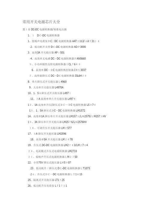
液晶电源管理芯片代换大全

MP2104 OCP2150-LTC3406/直接代换
AT1366/MP2104 直接代换
ACT6906-LTC3406/AT1366/直接代换
MP2104 OCP2160-LTC3407直接代换
ACT4065-ZA3020/MP1580 直接代换
1200AP40 1200AP60、1203P60
200D6、203D6 DAP8A 可互代
203D6/1203P6 DAP8A
2S0680 2S0880
3S0680 3S0880
5S0765 DP104、DP704
8S0765C DP704加24V的稳压二极管
ACT4060 ZA3020LV/MP1410/MP9141
电源IC(ZSTR-G5643D G5653D G8653D 直接代换
203D6/1203P6和DAP8A 直接代换 DM0465R。DM0565R用cm0565r代换成功 (取掉4脚的稳压二极管)
LD7575PS 可用203D6代(没试过,只是1脚的对地电阻不同,改了就可了)
LD7552可用SG6841代(不过要改4脚电阻,)
STR G5653直接用STR G8656代换 试验成功!
. FSCQ1565>1265>0765>0565
FS5Q1565>1265>0765>0565
5Q系列供电为20V,CQ系列供电为18V,5Q代换CQ系列时需拆除那个稳压二极管,短接10欧姆电阻!
STRG8656>8654>5653
OCP2160 LTC3407
OCP2576 LM2576
常用的开关电源芯片大全

常用开关电源芯片大全第1章DC-DC电源转换器/基准电压源1.1 DC-DC电源转换器1.低噪声电荷泵DC-DC电源转换器AAT3113/AAT31142.低功耗开关型DC-DC电源转换器ADP30003.高效3A开关稳压器AP15014.高效率无电感DC-DC电源转换器FAN56605.小功率极性反转电源转换器ICL76606.高效率DC-DC电源转换控制器IRU30377.高性能降压式DC-DC电源转换器ISL64208.单片降压式开关稳压器L49609.大功率开关稳压器L4970A10.1.5A降压式开关稳压器L497111.2A高效率单片开关稳压器L497812.1A高效率升压/降压式DC-DC电源转换器L597013.1.5A降压式DC-DC电源转换器LM157214.高效率1A降压单片开关稳压器LM1575/LM2575/LM2575HV15.3A降压单片开关稳压器LM2576/LM2576HV16.可调升压开关稳压器LM257717.3A降压开关稳压器LM259618.高效率5A开关稳压器LM267819.升压式DC-DC电源转换器LM2703/LM270420.电流模式升压式电源转换器LM273321.低噪声升压式电源转换器LM275022.小型75V降压式稳压器LM500723.低功耗升/降压式DC-DC电源转换器LT107324.升压式DC-DC电源转换器LT161525.隔离式开关稳压器LT172526.低功耗升压电荷泵LT175127.大电流高频降压式DC-DC电源转换器LT176528.大电流升压转换器LT193529.高效升压式电荷泵LT193730.高压输入降压式电源转换器LT195631.1.5A升压式电源转换器LT196132.高压升/降压式电源转换器LT343333.单片3A升压式DC-DC电源转换器LT343634.通用升压式DC-DC电源转换器LT346035.高效率低功耗升压式电源转换器LT346436.1.1A升压式DC-DC电源转换器LT346737.大电流高效率升压式DC-DC电源转换器LT378238.微型低功耗电源转换器LTC175439.1.5A单片同步降压式稳压器LTC187540.低噪声高效率降压式电荷泵LTC191141.低噪声电荷泵LTC3200/LTC3200-542.无电感的降压式DC-DC电源转换器LTC325143.双输出/低噪声/降压式电荷泵LTC325244.同步整流/升压式DC-DC电源转换器LTC340145.低功耗同步整流升压式DC-DC电源转换器LTC340246.同步整流降压式DC-DC电源转换器LTC340547.双路同步降压式DC-DC电源转换器LTC340748.高效率同步降压式DC-DC电源转换器LTC341649.微型2A升压式DC-DC电源转换器LTC342650.2A两相电流升压式DC-DC电源转换器LTC342851.单电感升/降压式DC-DC电源转换器LTC344052.大电流升/降压式DC-DC电源转换器LTC344253.1.4A同步升压式DC-DC电源转换器LTC345854.直流同步降压式DC-DC电源转换器LTC370355.双输出降压式同步DC-DC电源转换控制器LTC373656.降压式同步DC-DC电源转换控制器LTC377057.双2相DC-DC电源同步控制器LTC380258.高性能升压式DC-DC电源转换器MAX1513/MAX151459.精简型升压式DC-DC电源转换器MAX1522/MAX1523/MAX152460.高效率40V升压式DC-DC电源转换器MAX1553/MAX155461.高效率升压式LED电压调节器MAX1561/MAX159962.高效率5路输出DC-DC电源转换器MAX156563.双输出升压式DC-DC电源转换器MAX1582/MAX1582Y64.驱动白光LED的升压式DC-DC电源转换器MAX158365.高效率升压式DC-DC电源转换器MAX1642/MAX164366.2A降压式开关稳压器MAX164467.高效率升压式DC-DC电源转换器MAX1674/MAX1675/MAX167668.高效率双输出DC-DC电源转换器MAX167769.低噪声1A降压式DC-DC电源转换器MAX1684/MAX168570.高效率升压式DC-DC电源转换器MAX169871.高效率双输出降压式DC-DC电源转换器MAX171572.小体积升压式DC-DC电源转换器MAX1722/MAX1723/MAX172473.输出电流为50mA的降压式电荷泵MAX173074.升/降压式电荷泵MAX175975.高效率多路输出DC-DC电源转换器MAX180076.3A同步整流降压式稳压型MAX1830/MAX183177.双输出开关式LCD电源控制器MAX187878.电流模式升压式DC-DC电源转换器MAX189679.具有复位功能的升压式DC-DC电源转换器MAX194780.高效率PWM降压式稳压器MAX1992/MAX199381.大电流输出升压式DC-DC电源转换器MAX61882.低功耗升压或降压式DC-DC电源转换器MAX62983.PWM升压式DC-DC电源转换器MAX668/MAX66984.大电流PWM降压式开关稳压器MAX724/MAX72685.高效率升压式DC-DC电源转换器MAX756/MAX75786.高效率大电流DC-DC电源转换器MAX761/MAX76287.隔离式DC-DC电源转换器MAX8515/MAX8515A88.高性能24V升压式DC-DC电源转换器MAX872789.升/降压式DC-DC电源转换器MC33063A/MC34063A90.5A升压/降压/反向DC-DC电源转换器MC33167/MC3416791.低噪声无电感电荷泵MCP1252/MCP125392.高频脉宽调制降压稳压器MIC220393.大功率DC-DC升压电源转换器MIC229594.单片微型高压开关稳压器NCP1030/NCP103195.低功耗升压式DC-DC电源转换器NCP1400A96.高压DC-DC电源转换器NCP140397.单片微功率高频升压式DC-DC电源转换器NCP141098.同步整流PFM步进式DC-DC电源转换器NCP142199.高效率大电流开关电压调整器NCP1442/NCP1443/NCP1444/NCP1445 100.新型双模式开关稳压器NCP1501101.高效率大电流输出DC-DC电源转换器NCP1550102.同步降压式DC-DC电源转换器NCP1570103.高效率升压式DC-DC电源转换器NCP5008/NCP5009104.大电流高速稳压器RT9173/RT9173A105.高效率升压式DC-DC电源转换器RT9262/RT9262A106.升压式DC-DC电源转换器SP6644/SP6645107.低功耗升压式DC-DC电源转换器SP6691108.新型高效率DC-DC电源转换器TPS54350109.无电感降压式电荷泵TPS6050x110.高效率升压式电源转换器TPS6101x111.28V恒流白色LED驱动器TPS61042112.具有LDO输出的升压式DC-DC电源转换器TPS6112x113.低噪声同步降压式DC-DC电源转换器TPS6200x114.三路高效率大功率DC-DC电源转换器TPS75003115.高效率DC-DC电源转换器UCC39421/UCC39422116.PWM控制升压式DC-DC电源转换器XC6371117.白光LED驱动专用DC-DC电源转换器XC9116118.500mA同步整流降压式DC-DC电源转换器XC9215/XC9216/XC9217 119.稳压输出电荷泵XC9801/XC9802120.高效率升压式电源转换器ZXLB16001.2 线性/低压差稳压器121.具有可关断功能的多端稳压器BAXXX122.高压线性稳压器HIP5600123.多路输出稳压器KA7630/KA7631124.三端低压差稳压器LM2937125.可调输出低压差稳压器LM2991126.三端可调稳压器LM117/LM317127.低压降CMOS500mA线性稳压器LP38691/LP38693128.输入电压从12V到450V的可调线性稳压器LR8129.300mA非常低压降稳压器(VLDO)LTC3025130.大电流低压差线性稳压器LX8610131.200mA负输出低压差线性稳压器MAX1735132.150mA低压差线性稳压器MAX8875133.带开关控制的低压差稳压器MC33375134.带有线性调节器的稳压器MC33998135.1.0A低压差固定及可调正稳压器NCP1117136.低静态电流低压差稳压器NCP562/NCP563137.具有使能控制功能的多端稳压器PQxx138.五端可调稳压器SI-3025B/SI-3157B139.400mA低压差线性稳压器SPX2975140.五端线性稳压器STR20xx141.五端线性稳压器STR90xx142.具有复位信号输出的双路输出稳压器TDA8133143.具有复位信号输出的双路输出稳压器TDA8138/TDA8138A144.带线性稳压器的升压式电源转换器TPS6110x145.低功耗50mA低压降线性稳压器TPS760xx146.高输入电压低压差线性稳压器XC6202147.高速低压差线性稳压器XC6204148.高速低压差线性稳压器XC6209F149.双路高速低压差线性稳压器XC64011.3 基准电压源150.新型XFET基准电压源ADR290/ADR291/ADR292/ADR293151.低功耗低压差大输出电流基准电压源MAX610x152.低功耗1.2V基准电压源MAX6120153.2.5V精密基准电压源MC1403154.2.5V/4.096V基准电压源MCP1525/MCP1541155.低功耗精密低压降基准电压源REF30xx/REF31xx156.精密基准电压源TL431/KA431/TLV431A第2章AC-DC转换器及控制器1.厚膜开关电源控制器DP104C2.厚膜开关电源控制器DP308P3.DPA-Switch系列高电压功率转换控制器DPA423/DPA424/DPA425/DPA4264.电流型开关电源控制器FA13842/FA13843/FA13844/FA138455.开关电源控制器FA5310/FA53116.PWM开关电源控制器FAN75567.绿色环保的PWM开关电源控制器FAN76018.FPS型开关电源控制器FS6M07652R9.开关电源功率转换器FS6Sxx10.降压型单片AC-DC转换器HV-2405E11.新型反激准谐振变换控制器ICE1QS0112.PWM电源功率转换器KA1M088013.开关电源功率转换器KA2S0680/KA2S088014.电流型开关电源控制器KA38xx15.FPS型开关电源功率转换器KA5H0165R16.FPS型开关电源功率转换器KA5Qxx17.FPS型开关电源功率转换器KA5Sxx18.电流型高速PWM控制器L499019.具有待机功能的PWM初级控制器L599120.低功耗离线式开关电源控制器L659021.LINK SWITCH TN系列电源功率转换器LNK304/LNK305/LNK30622.LINK SWITCH系列电源功率转换器LNK500/LNK501/LNK52023.离线式开关电源控制器M51995A24.PWM电源控制器M62281P/M62281FP25.高频率电流模式PWM控制器MAX5021/MAX502226.新型PWM开关电源控制器MC4460427.电流模式开关电源控制器MC4460528.低功耗开关电源控制器MC4460829.具有PFC功能的PWM电源控制器ML482430.液晶显示器背光灯电源控制器ML487631.离线式电流模式控制器NCP120032.电流模式脉宽调制控制器NCP120533.准谐振式PWM控制器NCP120734.低成本离线式开关电源控制电路NCP121535.低待机能耗开关电源PWM控制器NCP123036.STR系列自动电压切换控制开关STR8xxxx37.大功率厚膜开关电源功率转换器STR-F665438.大功率厚膜开关电源功率转换器STR-G865639.开关电源功率转换器STR-M6511/STR-M652940.离线式开关电源功率转换器STR-S5703/STR-S5707/STR-S570841.离线式开关电源功率转换器STR-S6401/STR-S6401F/STR-S6411/STR-S6411F 442.开关电源功率转换器STR-S651343.离线式开关电源功率转换器TC33369~TC3337444.高性能PFC与PWM组合控制集成电路TDA16846/TDA1684745.新型开关电源控制器TDA1685046.“绿色”电源控制器TEA150447.第二代“绿色”电源控制器TEA150748.新型低功耗“绿色”电源控制器TEA153349.开关电源控制器TL494/KA7500/MB375950.Tiny SwitchⅠ系列功率转换器TNY253、TNY254、TNY25551.Tiny SwitchⅡ系列功率转换器TNY264P~TNY268G52.TOP Switch(Ⅱ)系列离线式功率转换器TOP209~TOP22753.TOP Switch-FX系列功率转换器TOP232/TOP233/TOP23454.TOP Switch-GX系列功率转换器TOP242~TOP25055.开关电源控制器UCX84X56.离线式开关电源功率转换器VIPer12AS/VIPer12ADIP57.新一代高度集成离线式开关电源功率转换器VIPer53第3章功率因数校正控制/节能灯电源控制器1.电子镇流器专用驱动电路BL83012.零电压开关功率因数控制器FAN48223.功率因数校正控制器FAN75274.高电压型EL背光驱动器HV8265.EL场致发光背光驱动器IMP525/IMP5606.高电压型EL背光驱动器/反相器IMP8037.电子镇流器自振荡半桥驱动器IR21568.单片荧光灯镇流器IR21579.调光电子镇流器自振荡半桥驱动器IR215910.卤素灯电子变压器智能控制电路IR216111.具有功率因数校正电路的镇流器电路IR216612.单片荧光灯镇流器IR216713.自适应电子镇流器控制器IR252014.电子镇流器专用控制器KA754115.功率因数校正控制器L656116.过渡模式功率因数校正控制器L656217.集成背景光控制器MAX8709/MAX8709A18.功率因数校正控制器MC33262/MC3426219.固定频率电流模式功率因数校正控制器NCP165320.EL场致发光灯高压驱动器SP440321.功率因数校正控制器TDA4862/TDA486322.有源功率因数校正控制器UC385423.高频自振荡节能灯驱动器电路VK05CFL24.大功率高频自振荡节能灯驱动器电路VK06TL第4章充电控制器1.多功能锂电池线性充电控制器AAT36802.可编程快速电池充电控制器BQ20003.可进行充电速率补偿的锂电池充电管理器BQ20574.锂电池充电管理电路BQ2400x5.单片锂电池线性充电控制器BQ2401xB接口单节锂电池充电控制器BQ2402x7.2A同步开关模式锂电池充电控制器BQ241008.集成PWM开关控制器的快速充电管理器BQ29549.具有电池电量计量功能的充电控制器DS277010.锂电池充电控制器FAN7563/FAN756411.2A线性锂/锂聚合物电池充电控制器ISL629212.锂电池充电控制器LA5621M/LA5621V13.1.5A通用充电控制器LT157114.2A恒流/恒压电池充电控制器LT176915.线性锂电池充电控制器LTC173216.带热调节功能的1A线性锂电池充电控制器LTC173317.线性锂电池充电控制器LTC173418.新型开关电源充电控制器LTC198019.开关模式锂电池充电控制器LTC400220.4A锂电池充电器LTC400621.多用途恒压/恒流充电控制器LTC400822.4.2V锂离子/锂聚合物电池充电控制器LTC405223.可由USB端口供电的锂电池充电控制器LTC405324.小型150mA锂电池充电控制器LTC405425.线性锂电池充电控制器LTC405826.单节锂电池线性充电控制器LTC405927.独立线性锂电池充电控制器LTC406128.镍镉/镍氢电池充电控制器M62256FP29.大电流锂/镍镉/镍氢电池充电控制器MAX150130.锂电池线性充电控制器MAX150731.双输入单节锂电池充电控制器MAX1551/MAX155532.单节锂电池充电控制器MAX167933.小体积锂电池充电控制器MAX1736B接口单节锂电池充电控制器MAX181135.多节锂电池充电控制器MAX187336.双路输入锂电池充电控制器MAX187437.单节锂电池线性充电控制器MAX189838.低成本/多种电池充电控制器MAX190839.开关模式单节锂电池充电控制器MAX1925/MAX192640.快速镍镉/镍氢充电控制器MAX2003A/MAX200341.可编程快速充电控制器MAX712/MAX71342.开关式锂电池充电控制器MAX74543.多功能低成本充电控制器MAX846A44.具有温度调节功能的单节锂电池充电控制器MAX8600/MAX860145.锂电池充电控制器MCP73826/MCP73827/MCP7382846.高精度恒压/恒流充电器控制器MCP73841/MCP73842/MCP73843/MCP73844 647.锂电池充电控制器MCP73861/MCP7386248.单节锂电池充电控制器MIC7905049.单节锂电池充电控制器NCP180050.高精度线性锂电池充电控制器VM7205。
LTC3407AEMSE-PBF资料

13407afaT YPICAL APPLICATIONF EATURESA PPLICATIONSD ESCRIPTION 1.5MHz Step-Down DC/DC RegulatorThe L TC ®3407A is a dual, constant frequency, synchronous step-down DC/DC converter . Intended for low power ap-plications, it operates from a 2.5V to 5.5V input voltage range and has a constant 1.5MHz switching frequency, enabling the use of tiny, low cost capacitors and inductors 1mm or less in height. Each output voltage is adjustable from 0.6V to 5V . Internal synchronous 0.35Ω, 1A power switches provide high effi ciency without the need for external Schottky diodes.A user selectable mode input is provided to allow the user to trade-off ripple noise for low power effi ciency. BurstMode ®operation provides the highest efficiency at light loads, while Pulse Skip Mode provides the lowest ripple noise at light loads.To further maximize battery life, the P-channel MOSFETs are turned on continuously in dropout (100% duty cycle), and both channels draw a total quiescent current of only 40μA. In shutdown, the device draws <1μA.1mm High 2.5V/1.8V at 600mA Step-Down RegulatorsnHigh Effi ciency: Up to 96%n Low Ripple (35mV P-P ) Burst Mode Operation;I Q = 40μAn 1.5MHz Constant Frequency Operation n No Schottky Diodes Required n Low R DS(ON) Internal Switches: 0.35Ωn Current Mode Operation for Excellent Line and Load T ransient Response n Short-C ircuit Protectedn Low Dropout Operation: 100% Duty Cycle n Ultralow Shutdown Current: I Q< 1μA n Output Voltages from 5V down to 0.6V n Power-On Reset Outputn Externally Synchronizable Oscillator n Optional External Soft-Startn Small Thermally Enhanced MSOP and 3mm × 3mm DFN PackagesnPDAs/Palmtop PC s n Digital C ameras n C ellular Phonesn Wireless and DSL ModemsL , L T , L TC, L TM and Burst Mode are registered trademarks of Linear Technology Corporation. All other trademarks are the property of their respective owners. Protected by U.S. Patents including 5481178, 6580258, 6304066, 6127815, 6498466, 6611131.L TC3407A Effi ciency/Power Loss CurveV OUT2OUT1= 1.8V 3407A TA01LOAD CURRENT (mA)1E F F I C I E N C Y (%)POWER LOSS (W)302010706050401000.00010.0010.10.01190801010010003407A TA0223407afaA BSOLUTE MAXIMUM RATINGS V IN Voltage ...................................................–0.3V to 6V V FB1, V FB2 Voltages ...................................–0.3V to 1.5V RUN/SS1, RUN/SS2 Voltages ......................–0.3V to V IN MODE/SYNC Voltage ....................................–0.3V to V IN SW1, SW2 Voltages .........................–0.3V to V IN + 0.3V POR Voltage .................................................–0.3V to 6V(Note 1)TOP VIEWDD PACKAGE10-LEAD (3mm × 3mm) PLASTIC DFN EXPOSED PAD IS PGND (PIN 11)MUST BE CONNECTED TO GND 1011967845321V FB2RUN/SS2POR SW2MODE/SYNCV FB1RUN/SS1V INSW1GNDT JMAX = 125°C, θJA = 45°C/W , θJC = 10°C/WTOP VIEW12345V FB1RUN/SS1V IN SW1GND109876V FB2RUN/SS2POR SW2MODE/SYNC11MSE PACKAGE10-LEAD PLASTIC MSOPEXPOSED PAD IS PGND (PIN 11)MUST BE CONNECTED TO GNDT JMAX = 125°C, θJA = 45°C/W , θJC = 10°C/WPIN CONFIGURATIONOperating Temperature Range (Note 2)L TC3407AE ..........................................–40°C to 85°C L TC3407AI .........................................–40°C to 125°C Junction Temperature (Note 5) .............................125°C Storage Temperature Range ...................–65°C to 150°C Lead Temperature (Soldering, 10 sec)L TC3407AMSE Only ..........................................300°CSYMBOL PARAMETERCONDITIONSMIN TYP MAX UNITSV IN Operating Voltage Range ● 2.5 5.5V I FB Feedback Pin Input Current ●30nA V FB Feedback Voltage (Note 3)0°C ≤ T A ≤ 85°C–40°C ≤ T A ≤ 125°C (L TC3407AI)●0.5880.5850.60.60.6120.612V V ΔV LINE REGReference Voltage Line RegulationV IN = 2.5V to 5.5V (Note 3)0.30.5%/VLEAD FREE FINISH TAPE AND REEL PART MARKING*PACKAGE DESCRIPTIONTEMPERATURE RANGE L TC3407AEDD#PBF L TC3407AEDD#TRPBF LCQN 10-Lead (3mm × 3mm) Plastic DFN –40°C to 85°C L TC3407AIDD#PBF L TC3407AIDD#TRPBF LCQN 10-Lead (3mm × 3mm) Plastic DFN –40°C to 125°C L TC3407AEMSE#PBF L TC3407AEMSE#TRPBF L TCRZ 10-Lead Plastic MSOP –40°C to 85°C L TC3407AIMSE#PBFL TC3407AIMSE#TRPBFL TCRZ10-Lead Plastic MSOP–40°C to 125°CConsult L TC Marketing for parts specifi ed with wider operating temperature ranges. *The temperature grade is identifi ed by a label on the shipping container .Consult L TC Marketing for information on non-standard lead based fi nish parts.For more information on lead free part marking, go to: http://www.linear .com/leadfree/ For more information on tape and reel specifi cations, go to: http://www.linear .com/tapeandreel/ORDER INFORMATIONELECTRICAL CHARACTERISTICSThe l denotes the specifi cations which apply over the full operating temperature range, otherwise specifi cations are at T A = 25°C. V IN = 3.6V , unless otherwise specifi ed. (Note 2)33407afaE LECTRICAL CHARACTERISTICS Note 1: Stresses beyond those listed under Absolute Maximum Ratings may cause permanent damage to the device. Exposure to any Absolute Maximum Rating condition for extended periods may affect device reliability and lifetime.Note 2: The L TC3407AE is guaranteed to meet specifi ed performance from 0°C to 85°C. Specifi cations over the –40°C and 85°C operatingtemperature range are assured by design, characterization and correlation with statistical process controls. The L TC3407AI is guaranteed over the full –40°C to 125°C temperature range.The l denotes the specifi cations which apply over the full operatingtemperature range, otherwise specifi cations are at T A = 25°C. V IN = 3.6V , unless otherwise specified. (Note 2)Note 3: The L TC3407A is tested in a proprietary test mode that connects V FB to the output of the error amplifi er .Note 4: Dynamic supply current is higher due to the internal gate charge being delivered at the switching frequency.Note 5: T J is calculated from the ambient T A and power dissipation P D according to the following formula: T J = T A + (P D • θJA ).Note 6: The DFN switch on-resistance is guaranteed by correlation to wafer level measurements.SYMBOL PARAMETERCONDITIONSMIN TYP MAX UNITSΔV LOAD REG Output Voltage Load Regulation MODE/SYNC = 0V (Note 3)0.5%I SInput DC Supply CurrentActive Mode Sleep Mode Shutdown (Note 4)V FB1 = V FB2 = 0.5VV FB1= V FB2 = 0.63V , MODE/SYNC = 3.6V RUN = 0V , V IN = 5.5V , MODE/SYNC = 0V 600400.1800601μA μA μA f OSC Oscillator Frequency V FBX = 0.6V●1.2 1.5 1.8MHz f SYNC Synchronization Frequency 1.5MHz I LIM Peak Switch Current Limit V IN = 3V , V FBX = 0.5V , Duty Cycle <35%0.751 1.25A R DS(ON)Top Switch On-Resistance Bottom Switch On-Resistance (Note 6)(Note 6)0.350.300.450.45ΩΩI SW(LKG)Switch Leakage Current V IN = 5V , V RUN = 0V , V FBX = 0V 0.011μA PORPower-On Reset Threshold V FBX Ramping Up, MODE/SYNC = 0V V FBX Ramping Down, MODE/SYNC = 0V8.5–8.5%%Power-On Reset On-Resistance 100200ΩPower-On Reset Delay65,536CyclesV RUN RUN/SS Threshold Low RUN/SS Threshold High ●●0.31 1.52V V I RUN RUN/SS Leakage Current ●0.011μA V MODEMODE Threshold Low 00.5V MODE Threshold HighV IN – 0.5V INVBurst Mode OperationPulse Skipping Mode3407 G01V IN = 3.6V V OUT = 1.8V I LOAD = 50mACIRCUIT OF FIGURE 3SW 5V/DIV V OUT 50mV/DIVI L200mA/DIV2μs/DIV3407 G02V IN = 3.6V V OUT = 1.8V I LOAD = 50mACIRCUIT OF FIGURE 3SW 5V/DIV V OUT 10mV/DIVI L100mA/DIV1μs/DIVTYPICAL PERFORMANCE CHARACTERISTICS43407afaT YPICAL PERFORMANCE CHARACTERISTICS Effi ciency vs Input VoltageOscillator Frequency vs TemperatureOscillator Frequency vs Supply VoltageReference Voltage vs TemperatureR DS(ON) vs Input VoltageR DS(ON) vs TemperatureT A = 25°C unless otherwise specifi ed.Load StepSoft Start3407 G03V IN = 3.6V V OUT = 1.8VI LOAD = 50mA TO 600mA CIRCUIT OF FIGURE 3V OUT2100mV/DIV V OUT1200mV/DIV I L500mA/DIV I LOAD 500mA/DIV20μs/DIV3407 G04V IN = 3.6V V OUT = 1.8V I LOAD = 500mACIRCUIT OF FIGURE 4V IN2V/DIV V OUT11V/DIV I L500mA/DIV1ms/DIVINPUT VOL TAGE (V)20E F F I C I E N C Y (%)1030405010070343407A G0520809060561.701.651.601.551.501.451.401.351.30F R E Q U E N C Y (M H z )TEMPERATURE (°C)–5025753407A G06–2550100125 1.81.71.61.51.41.31.2O S C I L L A T O R F R E Q U E N C Y (M H z )SUPPLY VOLTAGE (V)23407A G0734560.6150.6100.6050.6000.5950.5900.585R E F E R E N C E V O L T A G E (V )TEMPERATURE (°C)–5025753407A G08–2550100125V IN (V)1500450400350300250200463407A G092357R D S (O N ) (m Ω)TEMPERATURE (°C)–5055050045040035030025020015010025753407A G10–2550100150125R D S (O N ) (m Ω)53407afaEffi ciency vs Load CurrentEffi ciency vs Load CurrentLoad RegulationTYPICAL PERFORMANCE CHARACTERISTICSEffi ciency vs Load CurrentEffi ciency vs Load CurrentLine RegulationT A = 25°C unless otherwise specified.V FB1 (Pin 1): Output Feedback. Receives the feedback volt-age from the external resistive divider across the output. Nominal voltage for this pin is 0.6V .RUN/SS1 (Pin 2): Regulator 1 Enable and Soft-Start Input. Forcing this pin to V IN enables regulator 1, while forcing it to GND causes regulator 1 to shut down. Connect external RC -network with desired time-constant to enable soft-start feature. This pin must be driven; do not fl oat.V IN (Pin 3): Main Power Supply. Must be closely decoupled to GND.SW1 (Pin 4): Regulator 1 Switch Node Connection to the Inductor . This pin swings from V IN to GND.GND (Pin 5): Main Ground. Connect to the (–) terminal of C OUT , and (–) terminal of C IN .MODE/SYNC (Pin 6): Combination Mode Selection and Oscillator Synchronization. This pin controls the opera-tion of the device. When tied to V IN or GND, Burst Mode operation or pulse skipping mode is selected, respectively. Do not fl oat this pin. The oscillation frequency can be synchronized to an external oscillator applied to this pin and pulse skipping mode is automatically selected.PIN FUNCTIONSLOAD CURRENT (mA)1E F F I C I E N C Y (%)3020107060504010090801010010003407A G11LOAD CURRENT (mA)1E F F I C I E N C Y (%)3020107060504010090801010010003407A G12LOAD CURRENT (mA)1–4V O U T E R R O R (%)–310–1–24321010010003407A G13LOAD CURRENT (mA)10E F F I C I E N C Y (%)3020107060504010090801010010003407A G14LOAD CURRENT (mA)1E F F I C I E N C Y (%)3020107060504010090801010010003407A G15V IN (V)2V O U T E R R O R (%)0.50.40.30.20.10–0.1–0.2–0.3–0.4–0.5463407A G163563407afaPIN FUNCTIONSSW2 (Pin 7): Regulator 2 Switch Node Connection to the Inductor . This pin swings from V IN to GND.POR (Pin 8): Power-On Reset. This common-drain logic output is pulled to GND when the output voltage is not within ±8.5% of regulation and goes high after 216 clock cycles when both channels are within regulation.RUN/SS2 (Pin 9): Regulator 2 Enable and Soft-Start Input. Forcing this pin to V IN enables regulator 2, while forcing it to GND causes regulator 2 to shut down. Connect externalBLOCK DIAGRAMRC -Network with desired time-constant to enable soft-start feature. This pin must be driven; do not fl oat.V FB2 (Pin 10): Output Feedback. Receives the feedback voltage from the external resistive divider across the output. Nominal voltage for this pin is 0.6V .Exposed Pad (GND) (Pin 11): Power Ground. Connect to the (–) terminal of C OUT , and (–) terminal of C IN . Must be soldered to electrical ground on PCB.IN MODE/SYNCV FB1RUN/SS1RUN/SS2V FB2OPERATIONThe L TC3407A uses a constant frequency, current mode architecture. The operating frequency is set at 1.5MHz and can be synchronized to an external oscillator. Both channels share the same clock and run in-phase. To suit a variety of applications, the selectable MODE/SYNC pin allows the user to trade-off noise for effi ciency.The output voltage is set by an external divider returned to the V FB pins. An error amplifi er compares the divided output voltage with a reference voltage of 0.6V and adjusts the peak inductor current accordingly. Overvoltage and undervoltage comparators will pull the POR output low if the output voltage is not within ±8.5%. The POR output will go high after 65,536 clock cycles (about 44ms in pulse skipping mode) of achieving regulation.Main Control LoopDuring normal operation, the top power switch (P-channel MOSFET) is turned on at the beginning of a clock cycle when the V FB voltage is below the reference voltage. The current into the inductor and the load increases until the current limit is reached. The switch turns off and energy stored in the inductor fl ows through the bottom switch (N-channel MOSFET) into the load until the next clock cycle.The peak inductor current is controlled by the internally compensated I TH voltage, which is the output of the er-ror amplifi er.This amplifi er compares the V FB pin to the 0.6V reference. When the load current increases, the V FB voltage decreases slightly below the reference. This decrease causes the error amplifi er to increase the I TH voltage until the average inductor current matches the new load current.The main control loop is shut down by pulling the RUN/SS pin to ground.Low Current OperationT wo modes are available to control the operation of the L TC3407A at low currents. Both modes automatically switch from continuous operation to the selected mode when the load current is low.To optimize effi ciency, the Burst Mode operation can be selected. When the load is relatively light, the L TC3407A automatically switches into Burst Mode operation in which the PMOS switch operates intermittently based on load demand with a fi xed peak inductor current. By running cycles periodically, the switching losses which are domi-nated by the gate charge losses of the power MOSFETs are minimized. The main control loop is interrupted when the output voltage reaches the desired regulated value. A voltage comparator trips when I TH is below 0.65V, shutting off the switch and reducing the power. The output capaci-tor and the inductor supply the power to the load until I TH exceeds 0.65V, turning on the switch and the main control loop which starts another cycle.For lower ripple noise at low currents, the pulse skipping mode can be used. In this mode, the L TC3407A continues to switch at a constant frequency down to very low cur-rents, where it will begin skipping pulses.Dropout OperationWhen the input supply voltage decreases toward the output voltage, the duty cycle increases to 100% which is the dropout condition. In dropout, the PMOS switch is turned on continuously with the output voltage being equal to the input voltage minus the voltage drops across the internal P-channel MOSFET and the inductor.An important design consideration is that the R DS(ON) of the P-channel switch increases with decreasing input supply voltage (See Typical Performance Characteristics). Therefore, the user should calculate the power dissipation when the L TC3407A is used at 100% duty cycle with low input voltage (See Thermal Considerations in the Applica-tions Information Section).Low Supply OperationThe L TC3407A incorporates an undervoltage lockout circuit which shuts down the part when the input voltage drops below about 1.65V to prevent unstable operation.A general LTC3407A application circuit is shown in Figure 1. External component selection is driven by the load requirement, and begins with the selection of the inductor L. Once the inductor is chosen, C IN and C OUT can be selected.73407afa83407afaInductor SelectionAlthough the inductor does not infl uence the operat-ing frequency, the inductor value has a direct effect on ripple current. The inductor ripple current ΔI L decreases with higher inductance and increases with higher V IN or V OUT :I L =VOUT f O •L •1–V OUT V INAccepting larger values of ΔI L allows the use of low inductances, but results in higher output voltage ripple, greater core losses, and lower output current capability. A reasonable starting point for setting ripple current is ΔI L = 0.3 • I LIM , where I LIM is the peak switch current limit. The largest ripple current ΔI L occurs at the maximum input voltage. To guarantee that the ripple current stays below a specifi ed maximum, the inductor value should be chosen according to the following equation:L =V OUT f O • I L •1–V OUT V IN(MAX) The inductor value will also have an effect on Burst Mode operation. The transition from low current operation begins when the peak inductor current falls below a level set by the burst clamp. Lower inductor values result in higher ripple current which causes this transition to occur at lower load currents. This causes a dip in effi ciency in the upper range of low current operation. In Burst Mode operation, lower inductance values will cause the burst frequency to increase.Inductor Core SelectionDifferent core materials and shapes will change the size/ current and price/current relationship of an inductor . Toroid or shielded pot cores in ferrite or permalloy materials are small and don’t radiate much energy, but generally cost more than powdered iron core inductors with similar elec-trical characterisitics. The choice of which style inductor to use often depends more on the price vs size require-ments and any radiated fi eld/EMI requirements than on what the L TC3407A requires to operate. Table 1 shows some typical surface mount inductors that work well in L TC3407A applications.Table 1. Representative Surface Mount InductorsMANUF-ACTURER PART NUMBER VALUE MAX DCCURRENT DCR HEIGHT Taiyo Yuden CB2016T2R2M CB2012T2R2M CB2016T3R3M 2.2μH 2.2μH 3.3μH 510mA 530mA 410mA 0.13Ω0.33Ω0.27Ω 1.6mm 1.25mm 1.6mm Panasonic EL T5KT4R7M 4.7μH 950mA 0.2Ω 1.2mm Sumida CDRH2D18/LD 4.7μH 630mA 0.086Ω2mm Murata LQH32CN4R7M23 4.7μH450mA 0.2Ω2mm Taiyo Yuden NR30102R2M NR30104R7M 2.2μH 4.7μH 1100mA 750mA 0.1Ω0.19Ω1mm 1mm FDKFDKMIPF2520D FDKMIPF2520D FDKMIPF2520D 4.7μH 3.3μH 2.2μH 1100mA 1200mA 1300mA 0.11Ω0.1Ω0.08Ω1mm 1mm 1mm TDKVLF3010AT4R7-MR70VLF3010AT3R3-MR87VLF3010AT2R2-M1R04.7μH 3.3μH 2.2μH700mA 870mA 1000mA0.28Ω0.17Ω0.12Ω1mm 1mm 1mmInput Capacitor (C IN ) SelectionIn continuous mode, the input current of the converter is a square wave with a duty cycle of approximately V OUT /V IN . To prevent large voltage transients, a low equivalent series resistance (ESR) input capacitor sized for the maximum RMS current must be used. The maximum RMS capacitor current is given by:I RMS ≈I MAXINwhere the maximum average output current I MAX equals the peak current minus half the peak-to-peak ripple cur-rent, I MAX = I LIM – ΔI L /2.APPLICATIONS INFORMATIONFigure 1. L TC3407A General Schematic3407A F01*MODE/SYNC = 0V: PULSE SKIP MODE/SYNC = V IN : Burst ModeA PPLICATIONS INFORMATIONThis formula has a maximum at V IN = 2V OUT, where I RMS = I OUT/2. This simple worst-case is commonly used to design because even signifi cant deviations do not offer much relief. Note that capacitor manufacturer’s ripple cur-rent ratings are often based on only 2000 hours lifetime. This makes it advisable to further derate the capacitor, or choose a capacitor rated at a higher temperature than required. Several capacitors may also be paralleled to meet the size or height requirements of the design. An additional 0.1μF to 1μF ceramic capacitor is also recommended on V IN for high frequency decoupling, when not using an all ceramic capacitor solution.Output Capacitor (C OUT) SelectionThe selection of C OUT is driven by the required ESR to minimize voltage ripple and load step transients. Typically, once the ESR requirement is satisfi ed, the capacitance is adequate for filtering. The output ripple (ΔV OUT) is determined by:V OUT I L ESR+18f O C OUTwhere f O = operating frequency, C OUT = output capacitance and ΔI L = ripple current in the inductor. The output ripple is highest at maximum input voltage since ΔI L increases with input voltage. With ΔI L = 0.3 • I LIM the output ripple will be less than 100mV at maximum V IN and f O = 1.5MHz with:ESR COUT < 150mΩOnce the ESR requirements for C OUT have been met, the RMS current rating generally far exceeds the I RIPPLE(P-P) requirement, except for an all ceramic solution.In surface mount applications, multiple capacitors may have to be paralleled to meet the capacitance, ESR or RMS current handling requirement of the application. Aluminum electrolytic, special polymer, ceramic and dry tantulum capacitors are all available in surface mount packages. The OS-C ON semiconductor dielectric capacitor available from Sanyo has the lowest ESR(size) product of any aluminum electrolytic at a somewhat higher price. Special polymer capacitors, such as Sanyo POSCAP, of-fer very low ESR, but have a lower capacitance density than other types. Tantalum capacitors have the highest capacitance density. However, they also have a larger ESR and it is critical that they are surge tested for use in switching power supplies. An excellent choice is the AVX TPS series of surface mount tantalums, available in case heights ranging from 2mm to 4mm. Aluminum electrolytic capacitors have a signifi cantly larger ESR, and are often used in extremely cost-sensitive applications provided that consideration is given to ripple current ratings and long term reliability. Ceramic capacitors have the lowest ESR and cost, but also have the lowest capacitance density, a high voltage and temperature coeffi cient, and exhibit audible piezoelectric effects. In addition, the high Q of ceramic capacitors along with trace inductance can lead to signifi cant ringing. Other capacitor types include the Panasonic Special Polymer (SP) capacitors.In most cases, 0.1μF to 1μF of ceramic capacitors should also be placed close to the L TC3407A in parallel with the main capacitors for high frequency decoupling. Ceramic Input and Output CapacitorsHigher value, lower cost ceramic capacitors are now be-coming available in smaller case sizes. These are tempting for switching regulator use because of their very low ESR. Unfortunately, the ESR is so low that it can cause loop stability problems. Solid tantalum capacitor ESR gener-ates a loop “zero” at 5kHz to 50kHz that is instrumental in giving acceptable loop phase margin. Ceramic capacitors remain capacitive to beyond 300kHz and usually resonate with their ESL before ESR becomes effective. Also, ceramic caps are prone to temperature effects which requires the designer to check loop stability over the operating tem-perature range. To minimize their large temperature and voltage coeffi cients, only X5R or X7R ceramic capacitors should be used. A good selection of ceramic capacitors is available from Taiyo Yuden, TDK, and Murata.Great care must be taken when using only ceramic input and output capacitors. When a ceramic capacitor is used at the input and the power is being supplied through long wires, such as from a wall adapter, a load step at the output can induce ringing at the V IN pin. At best, this ringing can couple to the output and be mistaken as loop instability. At worst, the ringing at the input can be large enough to damage the part.93407afa103407afaAPPLICATIONS INFORMATIONSince the ESR of a ceramic capacitor is so low, the input and output capacitor must instead fulfi ll a charge storage requirement. During a load step, the output capacitor must instantaneously supply the current to support the load until the feedback loop raises the switch current enough to support the load. The time required for the feedback loop to respond is dependent on the compensation and the output capacitor size. Typically, 3-4 cycles are required to respond to a load step, but only in the fi rst cycle does the output drop linearly. The output droop, V DROOP , is usually about 3 times the linear drop of the fi rst cycle. Thus, a good place to start is with the output capacitor size of approximately:C OUT ≈3ΔI OUTf O •V DROOPMore capacitance may be required depending on the duty cycle and load step requirements.In most applications, the input capacitor is merely required to supply high frequency bypassing, since the impedance to the supply is very low. A 10μF ceramic capacitor is usually enough for these conditions.Setting the Output VoltageThe L TC3407A develops a 0.6V reference voltage between the feedback pin, V FB , and ground as shown in Figure 1. The output voltage is set by a resistive divider according to the following formula:V OUT =0.6V 1+R2R1Keeping the current small (<5μA) in these resistors maxi-mizes effi ciency, but making them too small may allow stray capacitance to cause noise problems and reduce the phase margin of the error amp loop.To improve the frequency response, a feed-forward capaci-tor C F may also be used. Great care should be taken to route the V FB line away from noise sources, such as the inductor or the SW line.Power-On ResetThe POR pin is an open-drain output which pulls low when either regulator is out of regulation. When both output voltages are within ±8.5% of regulation, a timer is started which releases POR after 216 clock cycles (about 44ms in pulse skipping mode). This delay can be signifi cantly longer in Burst Mode operation with low load currents, since the clock cycles only occur during a burst and there could be milliseconds of time between bursts. This can be bypassed by tying the POR output to the MODE/SYNC input, to force pulse skipping mode during a reset. In addition, if the output voltage faults during Burst Mode sleep, POR could have a slight delay for an undervoltage output condition and may not respond to an overvoltage output. This can be avoided by using pulse skipping mode instead. When either channel is shut down, the POR output is pulled low, since one or both of the channels are not in regulation.Mode Selection & Frequency Synchronization The MODE/SYNC pin is a multipurpose pin which provides mode selection and frequency synchronization. Connect-ing this pin to V IN enables Burst Mode operation, which provides the best low current effi ciency at the cost of a higher output voltage ripple. When this pin is connected to ground, pulse skipping operation is selected which provides the lowest output ripple, at the cost of low cur-rent effi ciency. The LTC 3407A can also be synchronized to another L TC3407A by the MODE/SYNC pin. During synchroniza-tion, the mode is set to pulse skipping and the top switch turn-on is synchronized to the rising edge of the external clock.Checking T ransient ResponseThe regulator loop response can be checked by look-ing at the load transient response. Switching regulators take several cycles to respond to a step in load current. When a load step occurs, V OUT immediately shifts by an amount equal to ΔI LOAD • ESR, where ESR is the effective series resistance of C OUT . ΔI LOAD also begins to charge or discharge C OUT generating a feedback error signal used by the regulator to return V OUT to its steady-state value.。
常用开关电源芯片大全
常用开关电源芯片大全第1章DC-DC电源转换器/基准电压源1。
1DC-DC电源转换器1、低噪声电荷泵DC—DC电源转换器AAT3113/AAT31142。
低功耗开关型DC-DC电源转换器ADP30003。
高效3A开关稳压器AP15014、高效率无电感DC—DC电源转换器FAN56605、小功率极性反转电源转换器ICL76606。
高效率DC—DC电源转换控制器IRU30377、高性能降压式DC—DC电源转换器ISL64208。
单片降压式开关稳压器L49609、大功率开关稳压器L4970A10、1。
5A降压式开关稳压器L497111。
2A高效率单片开关稳压器L497812、1A高效率升压/降压式DC—DC电源转换器L597013。
1、5A降压式DC-DC电源转换器LM157214、高效率1A降压单片开关稳压器LM1575/LM2575/LM2575HV15、3A降压单片开关稳压器LM2576/LM2576HV16。
可调升压开关稳压器LM257717。
3A降压开关稳压器LM259618、高效率5A开关稳压器LM267819。
升压式DC-DC电源转换器LM2703/LM270420、电流模式升压式电源转换器LM273321。
低噪声升压式电源转换器LM275022。
小型75V降压式稳压器LM500723、低功耗升/降压式DC-DC电源转换器LT107324、升压式DC—DC电源转换器LT161525、隔离式开关稳压器LT172526、低功耗升压电荷泵LT175127、大电流高频降压式DC—DC电源转换器LT176528、大电流升压转换器LT193529、高效升压式电荷泵LT193730。
高压输入降压式电源转换器LT195631。
1。
5A升压式电源转换器LT196132、高压升/降压式电源转换器LT343333。
单片3A升压式DC—DC电源转换器LT343634、通用升压式DC-DC电源转换器LT346035、高效率低功耗升压式电源转换器LT346436、1。
LCDHome论坛_电源模块代换大全
液晶电源管理芯片代换大全1200AP40 1200AP60、1203P60200D6、203D6 DAP8A 可互代203D6/1203P6 DAP8A2S0680 2S08803S0680 3S08805S0765 DP104、DP7048S0765C DP704加24V的稳压二极管ACT4060 ZA3020LV/MP1410/MP9141ACT4065 ZA3020/MP1580ACT4070 ZA3030/MP1583/MP1591MP1593/MP1430ACT6311 LT1937ACT6906 LTC3406/AT1366/MP2104AMC2576 LM2576AMC2596 LM2596AMC3100 LTC3406/AT1366/MP2104AMC34063A AMC34063AMC7660 AJC1564AP8012 VIPer12AAP8022 VIPer22ADAP02 可用SG5841 /SG6841代换DAP02ALSZ SG6841DAP02ALSZ SG6841DAP7A、DP8A 203D6、1203P6DH321、DL321 Q100、DM0265RDM0465R DM/CM0565RDM0465R/DM0565R 用cm0565r代换(取掉4脚的稳压二极管)DP104 5S0765DP704 5S0765DP706 5S0765DP804 DP904FAN7601 LAF0001LD7552 可用SG6841代(改4脚电阻)LD7575PS 203D6改1脚100K电阻为24KOB2268CP OB2269CPOB2268CP SG6841改4脚100K电阻为20-47KOCP1451 TL1451/BA9741/SP9741/AP200OCP2150 LTC3406/AT1366/MP2104OCP2160 LTC3407坂面精通家电维修中心电话0598-OCP2576 LM2576OCP3601 MB3800OCP5001 TL5001OMC2596 LM2596/AP1501PT1301 RJ9266PT4101 AJC1648/MP3202PT4102 LT1937/AJC1896/AP1522/RJ9271/MP1540SG5841SZ SG6841DZ/SG6841DSM9621 RJ9621/AJC1642SP1937 LT1937/AJC1896/AP1522/RJ9271/MP1540STR-G5643D STR-G5653D、STR-G8653DTEA1507 TEA1533TEA1530 TEA1532对应引脚功能接入THX202H TFC719THX203H TFC718STOP246Y TOP247YVA7910 MAX1674/75 L6920 AJC1610VIPer12A VIPer22A[audio01]ICE2A165(1A/650V.31W);ICE2A265(2A/650V.52W);ICE2B0565(0.5A/650V.23W):ICE2B165(1A/650V.31W);ICE2B265(2A/650V.52W);ICE2A180(1A/800V.29W);ICE2A280(2A/800.50W).KA5H0365R, KA5M0365R, KA5L0365R, KA5M0365RN# u) t! u1 W1 B) R, PKA5L0365RN, KA5H0380R, KA5M0380R, KA5L0380R1、KA5Q1265RF/RT(大小两种体积)、KA5Q0765、FSCQ1265RT、KACQ1265RF、FSCQ0765RT、FSCQ1565Q这是一类的,这些型号的引脚功能全都一样,只是输出功率不一样。
常用开关电源芯片大全

常用开关电源芯片大全————————————————————————————————作者:————————————————————————————————日期:常用开关电源芯片大全第1章DC-DC电源转换器/基准电压源1.1 DC-DC电源转换器1.低噪声电荷泵DC-DC电源转换器AAT3113/AAT31142.低功耗开关型DC-DC电源转换器ADP30003.高效3A开关稳压器AP15014.高效率无电感DC-DC电源转换器FAN56605.小功率极性反转电源转换器ICL76606.高效率DC-DC电源转换控制器IRU30377.高性能降压式DC-DC电源转换器ISL64208.单片降压式开关稳压器L49609.大功率开关稳压器L4970A10.1.5A降压式开关稳压器L497111.2A高效率单片开关稳压器L497812.1A高效率升压/降压式DC-DC电源转换器L597013.1.5A降压式DC-DC电源转换器LM157214.高效率1A降压单片开关稳压器LM1575/LM2575/LM2575HV15.3A降压单片开关稳压器LM2576/LM2576HV16.可调升压开关稳压器LM257717.3A降压开关稳压器LM259618.高效率5A开关稳压器LM267819.升压式DC-DC电源转换器LM2703/LM270420.电流模式升压式电源转换器LM273321.低噪声升压式电源转换器LM275022.小型75V降压式稳压器LM500723.低功耗升/降压式DC-DC电源转换器LT107324.升压式DC-DC电源转换器LT161525.隔离式开关稳压器LT172526.低功耗升压电荷泵LT175127.大电流高频降压式DC-DC电源转换器LT176528.大电流升压转换器LT193529.高效升压式电荷泵LT193730.高压输入降压式电源转换器LT195631.1.5A升压式电源转换器LT196132.高压升/降压式电源转换器LT343333.单片3A升压式DC-DC电源转换器LT343634.通用升压式DC-DC电源转换器LT346035.高效率低功耗升压式电源转换器LT346436.1.1A升压式DC-DC电源转换器LT346737.大电流高效率升压式DC-DC电源转换器LT378238.微型低功耗电源转换器LTC175439.1.5A单片同步降压式稳压器LTC187540.低噪声高效率降压式电荷泵LTC191141.低噪声电荷泵LTC3200/LTC3200-542.无电感的降压式DC-DC电源转换器LTC325143.双输出/低噪声/降压式电荷泵LTC325244.同步整流/升压式DC-DC电源转换器LTC340145.低功耗同步整流升压式DC-DC电源转换器LTC340246.同步整流降压式DC-DC电源转换器LTC340547.双路同步降压式DC-DC电源转换器LTC340748.高效率同步降压式DC-DC电源转换器LTC341649.微型2A升压式DC-DC电源转换器LTC342650.2A两相电流升压式DC-DC电源转换器LTC342851.单电感升/降压式DC-DC电源转换器LTC344052.大电流升/降压式DC-DC电源转换器LTC344253.1.4A同步升压式DC-DC电源转换器LTC345854.直流同步降压式DC-DC电源转换器LTC370355.双输出降压式同步DC-DC电源转换控制器LTC373656.降压式同步DC-DC电源转换控制器LTC377057.双2相DC-DC电源同步控制器LTC380258.高性能升压式DC-DC电源转换器MAX1513/MAX151459.精简型升压式DC-DC电源转换器MAX1522/MAX1523/MAX152460.高效率40V升压式DC-DC电源转换器MAX1553/MAX155461.高效率升压式LED电压调节器MAX1561/MAX159962.高效率5路输出DC-DC电源转换器MAX156563.双输出升压式DC-DC电源转换器MAX1582/MAX1582Y64.驱动白光LED的升压式DC-DC电源转换器MAX158365.高效率升压式DC-DC电源转换器MAX1642/MAX164366.2A降压式开关稳压器MAX164467.高效率升压式DC-DC电源转换器MAX1674/MAX1675/MAX167668.高效率双输出DC-DC电源转换器MAX167769.低噪声1A降压式DC-DC电源转换器MAX1684/MAX168570.高效率升压式DC-DC电源转换器MAX169871.高效率双输出降压式DC-DC电源转换器MAX171572.小体积升压式DC-DC电源转换器MAX1722/MAX1723/MAX172473.输出电流为50mA的降压式电荷泵MAX173074.升/降压式电荷泵MAX175975.高效率多路输出DC-DC电源转换器MAX180076.3A同步整流降压式稳压型MAX1830/MAX183177.双输出开关式LCD电源控制器MAX187878.电流模式升压式DC-DC电源转换器MAX189679.具有复位功能的升压式DC-DC电源转换器MAX194780.高效率PWM降压式稳压器MAX1992/MAX199381.大电流输出升压式DC-DC电源转换器MAX61882.低功耗升压或降压式DC-DC电源转换器MAX62983.PWM升压式DC-DC电源转换器MAX668/MAX66984.大电流PWM降压式开关稳压器MAX724/MAX72685.高效率升压式DC-DC电源转换器MAX756/MAX75786.高效率大电流DC-DC电源转换器MAX761/MAX76287.隔离式DC-DC电源转换器MAX8515/MAX8515A88.高性能24V升压式DC-DC电源转换器MAX872789.升/降压式DC-DC电源转换器MC33063A/MC34063A90.5A升压/降压/反向DC-DC电源转换器MC33167/MC3416791.低噪声无电感电荷泵MCP1252/MCP125392.高频脉宽调制降压稳压器MIC220393.大功率DC-DC升压电源转换器MIC229594.单片微型高压开关稳压器NCP1030/NCP103195.低功耗升压式DC-DC电源转换器NCP1400A96.高压DC-DC电源转换器NCP140397.单片微功率高频升压式DC-DC电源转换器NCP141098.同步整流PFM步进式DC-DC电源转换器NCP142199.高效率大电流开关电压调整器NCP1442/NCP1443/NCP1444/NCP1445 100.新型双模式开关稳压器NCP1501101.高效率大电流输出DC-DC电源转换器NCP1550102.同步降压式DC-DC电源转换器NCP1570103.高效率升压式DC-DC电源转换器NCP5008/NCP5009104.大电流高速稳压器RT9173/RT9173A105.高效率升压式DC-DC电源转换器RT9262/RT9262A106.升压式DC-DC电源转换器SP6644/SP6645107.低功耗升压式DC-DC电源转换器SP6691108.新型高效率DC-DC电源转换器TPS54350109.无电感降压式电荷泵TPS6050x110.高效率升压式电源转换器TPS6101x111.28V恒流白色LED驱动器TPS61042112.具有LDO输出的升压式DC-DC电源转换器TPS6112x113.低噪声同步降压式DC-DC电源转换器TPS6200x114.三路高效率大功率DC-DC电源转换器TPS75003115.高效率DC-DC电源转换器UCC39421/UCC39422116.PWM控制升压式DC-DC电源转换器XC6371117.白光LED驱动专用DC-DC电源转换器XC9116118.500mA同步整流降压式DC-DC电源转换器XC9215/XC9216/XC9217 119.稳压输出电荷泵XC9801/XC9802120.高效率升压式电源转换器ZXLB16001.2 线性/低压差稳压器121.具有可关断功能的多端稳压器BAXXX122.高压线性稳压器HIP5600123.多路输出稳压器KA7630/KA7631124.三端低压差稳压器LM2937125.可调输出低压差稳压器LM2991126.三端可调稳压器LM117/LM317127.低压降CMOS500mA线性稳压器LP38691/LP38693128.输入电压从12V到450V的可调线性稳压器LR8129.300mA非常低压降稳压器(VLDO)LTC3025130.大电流低压差线性稳压器LX8610131.200mA负输出低压差线性稳压器MAX1735132.150mA低压差线性稳压器MAX8875133.带开关控制的低压差稳压器MC33375134.带有线性调节器的稳压器MC33998135.1.0A低压差固定及可调正稳压器NCP1117136.低静态电流低压差稳压器NCP562/NCP563137.具有使能控制功能的多端稳压器PQxx138.五端可调稳压器SI-3025B/SI-3157B139.400mA低压差线性稳压器SPX2975140.五端线性稳压器STR20xx141.五端线性稳压器STR90xx142.具有复位信号输出的双路输出稳压器TDA8133143.具有复位信号输出的双路输出稳压器TDA8138/TDA8138A144.带线性稳压器的升压式电源转换器TPS6110x145.低功耗50mA低压降线性稳压器TPS760xx146.高输入电压低压差线性稳压器XC6202147.高速低压差线性稳压器XC6204148.高速低压差线性稳压器XC6209F149.双路高速低压差线性稳压器XC64011.3 基准电压源150.新型XFET基准电压源ADR290/ADR291/ADR292/ADR293151.低功耗低压差大输出电流基准电压源MAX610x152.低功耗1.2V基准电压源MAX6120153.2.5V精密基准电压源MC1403154.2.5V/4.096V基准电压源MCP1525/MCP1541155.低功耗精密低压降基准电压源REF30xx/REF31xx156.精密基准电压源TL431/KA431/TLV431A第2章AC-DC转换器及控制器1.厚膜开关电源控制器DP104C2.厚膜开关电源控制器DP308P3.DPA-Switch系列高电压功率转换控制器DPA423/DPA424/DPA425/DPA4264.电流型开关电源控制器FA13842/FA13843/FA13844/FA138455.开关电源控制器FA5310/FA53116.PWM开关电源控制器FAN75567.绿色环保的PWM开关电源控制器FAN76018.FPS型开关电源控制器FS6M07652R9.开关电源功率转换器FS6Sxx10.降压型单片AC-DC转换器HV-2405E11.新型反激准谐振变换控制器ICE1QS0112.PWM电源功率转换器KA1M088013.开关电源功率转换器KA2S0680/KA2S088014.电流型开关电源控制器KA38xx15.FPS型开关电源功率转换器KA5H0165R16.FPS型开关电源功率转换器KA5Qxx17.FPS型开关电源功率转换器KA5Sxx18.电流型高速PWM控制器L499019.具有待机功能的PWM初级控制器L599120.低功耗离线式开关电源控制器L659021.LINK SWITCH TN系列电源功率转换器LNK304/LNK305/LNK30622.LINK SWITCH系列电源功率转换器LNK500/LNK501/LNK52023.离线式开关电源控制器M51995A24.PWM电源控制器M62281P/M62281FP25.高频率电流模式PWM控制器MAX5021/MAX502226.新型PWM开关电源控制器MC4460427.电流模式开关电源控制器MC4460528.低功耗开关电源控制器MC4460829.具有PFC功能的PWM电源控制器ML482430.液晶显示器背光灯电源控制器ML487631.离线式电流模式控制器NCP120032.电流模式脉宽调制控制器NCP120533.准谐振式PWM控制器NCP120734.低成本离线式开关电源控制电路NCP121535.低待机能耗开关电源PWM控制器NCP123036.STR系列自动电压切换控制开关STR8xxxx37.大功率厚膜开关电源功率转换器STR-F665438.大功率厚膜开关电源功率转换器STR-G865639.开关电源功率转换器STR-M6511/STR-M652940.离线式开关电源功率转换器STR-S5703/STR-S5707/STR-S570841.离线式开关电源功率转换器STR-S6401/STR-S6401F/STR-S6411/STR-S6411F 442.开关电源功率转换器STR-S651343.离线式开关电源功率转换器TC33369~TC3337444.高性能PFC与PWM组合控制集成电路TDA16846/TDA1684745.新型开关电源控制器TDA1685046.“绿色”电源控制器TEA150447.第二代“绿色”电源控制器TEA150748.新型低功耗“绿色”电源控制器TEA153349.开关电源控制器TL494/KA7500/MB375950.Tiny SwitchⅠ系列功率转换器TNY253、TNY254、TNY25551.Tiny SwitchⅡ系列功率转换器TNY264P~TNY268G52.TOP Switch(Ⅱ)系列离线式功率转换器TOP209~TOP22753.TOP Switch-FX系列功率转换器TOP232/TOP233/TOP23454.TOP Switch-GX系列功率转换器TOP242~TOP25055.开关电源控制器UCX84X56.离线式开关电源功率转换器VIPer12AS/VIPer12ADIP57.新一代高度集成离线式开关电源功率转换器VIPer53第3章功率因数校正控制/节能灯电源控制器1.电子镇流器专用驱动电路BL83012.零电压开关功率因数控制器FAN48223.功率因数校正控制器FAN75274.高电压型EL背光驱动器HV8265.EL场致发光背光驱动器IMP525/IMP5606.高电压型EL背光驱动器/反相器IMP8037.电子镇流器自振荡半桥驱动器IR21568.单片荧光灯镇流器IR21579.调光电子镇流器自振荡半桥驱动器IR215910.卤素灯电子变压器智能控制电路IR216111.具有功率因数校正电路的镇流器电路IR216612.单片荧光灯镇流器IR216713.自适应电子镇流器控制器IR252014.电子镇流器专用控制器KA754115.功率因数校正控制器L656116.过渡模式功率因数校正控制器L656217.集成背景光控制器MAX8709/MAX8709A18.功率因数校正控制器MC33262/MC3426219.固定频率电流模式功率因数校正控制器NCP165320.EL场致发光灯高压驱动器SP440321.功率因数校正控制器TDA4862/TDA486322.有源功率因数校正控制器UC385423.高频自振荡节能灯驱动器电路VK05CFL24.大功率高频自振荡节能灯驱动器电路VK06TL第4章充电控制器1.多功能锂电池线性充电控制器AAT36802.可编程快速电池充电控制器BQ20003.可进行充电速率补偿的锂电池充电管理器BQ20574.锂电池充电管理电路BQ2400x5.单片锂电池线性充电控制器BQ2401xB接口单节锂电池充电控制器BQ2402x7.2A同步开关模式锂电池充电控制器BQ241008.集成PWM开关控制器的快速充电管理器BQ29549.具有电池电量计量功能的充电控制器DS277010.锂电池充电控制器FAN7563/FAN756411.2A线性锂/锂聚合物电池充电控制器ISL629212.锂电池充电控制器LA5621M/LA5621V13.1.5A通用充电控制器LT157114.2A恒流/恒压电池充电控制器LT176915.线性锂电池充电控制器LTC173216.带热调节功能的1A线性锂电池充电控制器LTC173317.线性锂电池充电控制器LTC173418.新型开关电源充电控制器LTC198019.开关模式锂电池充电控制器LTC400220.4A锂电池充电器LTC400621.多用途恒压/恒流充电控制器LTC400822.4.2V锂离子/锂聚合物电池充电控制器LTC405223.可由USB端口供电的锂电池充电控制器LTC405324.小型150mA锂电池充电控制器LTC405425.线性锂电池充电控制器LTC405826.单节锂电池线性充电控制器LTC405927.独立线性锂电池充电控制器LTC406128.镍镉/镍氢电池充电控制器M62256FP29.大电流锂/镍镉/镍氢电池充电控制器MAX150130.锂电池线性充电控制器MAX150731.双输入单节锂电池充电控制器MAX1551/MAX155532.单节锂电池充电控制器MAX167933.小体积锂电池充电控制器MAX1736B接口单节锂电池充电控制器MAX181135.多节锂电池充电控制器MAX187336.双路输入锂电池充电控制器MAX187437.单节锂电池线性充电控制器MAX189838.低成本/多种电池充电控制器MAX190839.开关模式单节锂电池充电控制器MAX1925/MAX192640.快速镍镉/镍氢充电控制器MAX2003A/MAX200341.可编程快速充电控制器MAX712/MAX71342.开关式锂电池充电控制器MAX74543.多功能低成本充电控制器MAX846A44.具有温度调节功能的单节锂电池充电控制器MAX8600/MAX860145.锂电池充电控制器MCP73826/MCP73827/MCP7382846.高精度恒压/恒流充电器控制器MCP73841/MCP73842/MCP73843/MCP73844 647.锂电池充电控制器MCP73861/MCP7386248.单节锂电池充电控制器MIC7905049.单节锂电池充电控制器NCP180050.高精度线性锂电池充电控制器VM7205。
常用电源芯片大全

常用电源芯片大全第1章DC-DC电源转换器/基准电压源1.1 DC-DC电源转换器1.低噪声电荷泵DC-DC电源转换器AAT3113/AAT31142.低功耗开关型DC-DC电源转换器ADP30003.高效3A开关稳压器AP15014.高效率无电感DC-DC电源转换器FAN56605.小功率极性反转电源转换器ICL76606.高效率DC-DC电源转换控制器IRU30377.高性能降压式DC-DC电源转换器ISL64208.单片降压式开关稳压器L49609.大功率开关稳压器L4970AL497111.2A高效率单片开关稳压器L497812.1A高效率升压/降压式DC-DC电源转换器L5970LM157214.高效率1A降压单片开关稳压器LM1575/LM2575/LM2575HV15.3A降压单片开关稳压器LM2576/LM2576HV16.可调升压开关稳压器LM257717.3A降压开关稳压器LM259618.高效率5A开关稳压器LM267819.升压式DC-DC电源转换器LM2703/LM270420.电流模式升压式电源转换器LM273321.低噪声升压式电源转换器LM275022.小型75V降压式稳压器LM500723.低功耗升/降压式DC-DC电源转换器LT107324.升压式DC-DC电源转换器LT161525.隔离式开关稳压器LT172526.低功耗升压电荷泵LT175127.大电流高频降压式DC-DC电源转换器LT176528.大电流升压转换器LT193529.高效升压式电荷泵LT193730.高压输入降压式电源转换器LT195632.高压升/降压式电源转换器LT343333.单片3A升压式DC-DC电源转换器LT343634.通用升压式DC-DC电源转换器LT346035.高效率低功耗升压式电源转换器LT3464LT346737.大电流高效率升压式DC-DC电源转换器LT378238.微型低功耗电源转换器LTC1754LTC187540.低噪声高效率降压式电荷泵LTC191141.低噪声电荷泵LTC3200/LTC3200-542.无电感的降压式DC-DC电源转换器LTC325143.双输出/低噪声/降压式电荷泵LTC325244.同步整流/升压式DC-DC电源转换器LTC340145.低功耗同步整流升压式DC-DC电源转换器LTC340246.同步整流降压式DC-DC电源转换器LTC340547.双路同步降压式DC-DC电源转换器LTC340748.高效率同步降压式DC-DC电源转换器LTC341649.微型2A升压式DC-DC电源转换器LTC342650.2A两相电流升压式DC-DC电源转换器LTC342851.单电感升/降压式DC-DC电源转换器LTC344052.大电流升/降压式DC-DC电源转换器LTC344254.直流同步降压式DC-DC电源转换器LTC370355.双输出降压式同步DC-DC电源转换控制器LTC373656.降压式同步DC-DC电源转换控制器LTC377057.双2相DC-DC电源同步控制器LTC380258.高性能升压式DC-DC电源转换器MAX1513/MAX151459.精简型升压式DC-DC电源转换器MAX1522/MAX1523/MAX152460.高效率40V升压式DC-DC电源转换器MAX1553/MAX155461.高效率升压式LED电压调节器MAX1561/MAX159962.高效率5路输出DC-DC电源转换器MAX156563.双输出升压式DC-DC电源转换器MAX1582/MAX1582Y64.驱动白光LED的升压式DC-DC电源转换器MAX158365.高效率升压式DC-DC电源转换器MAX1642/MAX164366.2A降压式开关稳压器MAX164467.高效率升压式DC-DC电源转换器MAX1674/MAX1675/MAX167668.高效率双输出DC-DC电源转换器MAX167769.低噪声1A降压式DC-DC电源转换器MAX1684/MAX168570.高效率升压式DC-DC电源转换器MAX169871.高效率双输出降压式DC-DC电源转换器MAX171572.小体积升压式DC-DC电源转换器MAX1722/MAX1723/MAX172473.输出电流为50mA的降压式电荷泵MAX173074.升/降压式电荷泵MAX175975.高效率多路输出DC-DC电源转换器MAX180076.3A同步整流降压式稳压型MAX1830/MAX183177.双输出开关式LCD电源控制器MAX187878.电流模式升压式DC-DC电源转换器MAX189679.具有复位功能的升压式DC-DC电源转换器MAX194780.高效率PWM降压式稳压器MAX1992/MAX199381.大电流输出升压式DC-DC电源转换器MAX61882.低功耗升压或降压式DC-DC电源转换器MAX62983.PWM升压式DC-DC电源转换器MAX668/MAX66984.大电流PWM降压式开关稳压器MAX724/MAX72685.高效率升压式DC-DC电源转换器MAX756/MAX75786.高效率大电流DC-DC电源转换器MAX761/MAX76287.隔离式DC-DC电源转换器MAX8515/MAX8515A88.高性能24V升压式DC-DC电源转换器MAX872789.升/降压式DC-DC电源转换器MC33063A/MC34063A90.5A升压/降压/反向DC-DC电源转换器MC33167/MC3416791.低噪声无电感电荷泵MCP1252/MCP125392.高频脉宽调制降压稳压器MIC220393.大功率DC-DC升压电源转换器MIC229594.单片微型高压开关稳压器NCP1030/NCP103195.低功耗升压式DC-DC电源转换器NCP1400A96.高压DC-DC电源转换器NCP140397.单片微功率高频升压式DC-DC电源转换器NCP141098.同步整流PFM步进式DC-DC电源转换器NCP142199.高效率大电流开关电压调器NCP1442/NCP1443/NCP1444/NCP1445 100.新型双模式开关稳压器NCP1501101.高效率大电流输出DC-DC电源转换器NCP1550102.同步降压式DC-DC电源转换器NCP1570103.高效率升压式DC-DC电源转换器NCP5008/NCP5009104.大电流高速稳压器RT9173/RT9173A105.高效率升压式DC-DC电源转换器RT9262/RT9262A106.升压式DC-DC电源转换器SP6644/SP6645107.低功耗升压式DC-DC电源转换器SP6691108.新型高效率DC-DC电源转换器TPS54350109.无电感降压式电荷泵TPS6050x110.高效率升压式电源转换器TPS6101x111.28V恒流白色LED驱动器TPS61042112.具有LDO输出的升压式DC-DC电源转换器TPS6112x113.低噪声同步降压式DC-DC电源转换器TPS6200x114.三路高效率大功率DC-DC电源转换器TPS75003115.高效率DC-DC电源转换器UCC39421/UCC39422116.PWM控制升压式DC-DC电源转换器XC6371117.白光LED驱动专用DC-DC电源转换器XC9116118.500mA同步整流降压式DC-DC电源转换XC9215/XC9216/XC9217 119.稳压输出电荷泵XC9801/XC9802120.高效率升压式电源转换器ZXLB16001.2 线性/低压差稳压器121.具有可关断功能的多端稳压器BAXXX122.高压线性稳压器HIP5600123.多路输出稳压器KA7630/KA7631124.三端低压差稳压器LM2937125.可调输出低压差稳压器LM2991126.三端可调稳压器LM117/LM317127.低压降CMOS500mA线性稳压器LP38691/LP38693128.输入电压从12V到450V的可调线性稳压器LR8129.300mA非常低压降稳压器(VLDO)LTC3025130.大电流低压差线性稳压器LX8610131.200mA负输出低压差线性稳压器MAX1735132.150mA低压差线性稳压器MAX8875133.带开关控制的低压差稳压器MC33375134.带有线性调节器的稳压器MC33998136.低静态电流低压差稳压器NCP562/NCP563137.具有使能控制功能的多端稳压器PQxx138.五端可调稳压器SI-3025B/SI-3157B139.400mA低压差线性稳压器SPX2975140.五端线性稳压器STR20xx141.五端线性稳压器STR90xx142.具有复位信号输出的双路输出稳压器TDA8133143.具有复位信号输出的双路输出稳压器TDA8138/TDA8138A 144.带线性稳压器的升压式电源转换器TPS6110x145.低功耗50mA低压降线性稳压器TPS760xx146.高输入电压低压差线性稳压器XC6202147.高速低压差线性稳压器XC6204148.高速低压差线性稳压器XC6209F149.双路高速低压差线性稳压器XC64011.3 基准电压源150.新型XFET基准电压源ADR290/ADR291/ADR292/ADR293151.低功耗低压差大输出电流基准电压源MAX610x152.低功耗1.2V基准电压源MAX6120155.低功耗精密低压降基准电压源REF30xx/REF31xx156.精密基准电压源TL431/KA431/TLV431A第2章AC-DC转换器及控制器1.厚膜开关电源控制器DP104C2.厚膜开关电源控制器DP308P3.DPA-Switch系列高电压功率转换控制器DPA423/DPA424/DPA425/DPA4264.电流型开关电源控制器FA13842/FA13843/FA13844/FA138455.开关电源控制器FA5310/FA53116.PWM开关电源控制器FAN75567.绿色环保的PWM开关电源控制器FAN76018.FPS型开关电源控制器FS6M07652R9.开关电源功率转换器FS6Sxx10.降压型单片AC-DC转换器HV-2405E11.新型反激准谐振变换控制器ICE1QS0112.PWM电源功率转换器KA1M088013.开关电源功率转换器KA2S0680/KA2S088014.电流型开关电源控制器KA38xx15.FPS型开关电源功率转换器KA5H0165R16.FPS型开关电源功率转换器KA5Qxx17.FPS型开关电源功率转换器KA5Sxx18.电流型高速PWM控制器L499019.具有待机功能的PWM初级控制器L599120.低功耗离线式开关电源控制器L659021.LINK SWITCH TN系列电源功率转换器LNK304/LNK305/LNK30622.LINK SWITCH系列电源功率转换器LNK500/LNK501/LNK52023.离线式开关电源控制器M51995A24.PWM电源控制器M62281P/M62281FP25.高频率电流模式PWM控制器MAX5021/MAX502226.新型PWM开关电源控制器MC4460427.电流模式开关电源控制器MC4460528.低功耗开关电源控制器MC4460829.具有PFC功能的PWM电源控制器ML482430.液晶显示器背光灯电源控制器ML487631.离线式电流模式控制器NCP120032.电流模式脉宽调制控制器NCP120533.准谐振式PWM控制器NCP120734.低成本离线式开关电源控制电路NCP121535.低待机能耗开关电源PWM控制器NCP123036.STR系列自动电压切换控制开关STR8xxxx37.大功率厚膜开关电源功率转换器STR-F665438.大功率厚膜开关电源功率转换器STR-G865639.开关电源功率转换器STR-M6511/STR-M652940.离线式开关电源功率转换器STR-S5703/STR-S5707/STR-S570841.离线式开关电源功率转换器STR-S6401/STR-S6401F/STR-S6411/STR- S6411F42.开关电源功率转换器STR-S651343.离线式开关电源功率转换器TC33369~TC3337444.高性能PFC与PWM组合控制集成电路TDA16846/TDA1684745.新型开关电源控制器TDA1685046.“绿色”电源控制器TEA1504 447.第二代“绿色”电源控制器TEA150748.新型低功耗“绿色”电源控制器TEA153349.开关电源控制器TL494/KA7500/MB375950.Tiny SwitchⅠ系列功率转换器TNY253、TNY254、TNY25551.Tiny SwitchⅡ系列功率转换器TNY264P~TNY268G52.TOP Switch(Ⅱ)系列离线式功率转换器TOP209~TOP22753.TOP Switch-FX系列功率转换器TOP232/TOP233/TOP23454.TOP Switch-GX系列功率转换器TOP242~TOP25055.开关电源控制器UCX84X56.离线式开关电源功率转换器VIPer12AS/VIPer12ADIP57.新一代高度集成离线式开关电源功率转换器VIPer53第3章功率因数校正控制/节能灯电源控制器1.电子镇流器专用驱动电路BL83012.零电压开关功率因数控制器FAN48223.功率因数校正控制器FAN75274.高电压型EL背光驱动器HV8265.EL场致发光背光驱动器IMP525/IMP5606.高电压型EL背光驱动器/反相器IMP8037.电子镇流器自振荡半桥驱动器IR21568.单片荧光灯镇流器IR21579.调光电子镇流器自振荡半桥驱动器IR215910.卤素灯电子变压器智能控制电路IR216111.具有功率因数校正电路的镇流器电路IR216612.单片荧光灯镇流器IR216713.自适应电子镇流器控制器IR252014.电子镇流器专用控制器KA754115.功率因数校正控制器L656116.过渡模式功率因数校正控制器L656217.集成背景光控制器MAX8709/MAX8709A18.功率因数校正控制器MC33262/MC3426219.固定频率电流模式功率因数校正控制器NCP165320.EL场致发光灯高压驱动器SP440321.功率因数校正控制器TDA4862/TDA486322.有源功率因数校正控制器UC385423.高频自振荡节能灯驱动器电路VK05CFL24.大功率高频自振荡节能灯驱动器电路VK06TL第4章充电控制器1.多功能锂电池线性充电控制器AAT36802.可编程快速电池充电控制器BQ20003.可进行充电速率补偿的锂电池充电管理器BQ20574.锂电池充电管理电路BQ2400x5.单片锂电池线性充电控制器BQ2401xB接口单节锂电池充电控制器BQ2402x7.2A同步开关模式锂电池充电控制器BQ241008.集成PWM开关控制器的快速充电管理器BQ29549.具有电池电量计量功能的充电控制器DS277010.锂电池充电控制器FAN7563/FAN756411.2A线性锂/锂聚合物电池充电控制器ISL629212.锂电池充电控制器LA5621M/LA5621V14.2A恒流/恒压电池充电控制器LT176915.线性锂电池充电控制器LTC173216.带热调节功能的1A线性锂电池充电控制器LTC173317.线性锂电池充电控制器LTC173418.新型开关电源充电控制器LTC198019.开关模式锂电池充电控制器LTC400220.4A锂电池充电器LTC400621.多用途恒压/恒流充电控制器LTC400823.可由USB端口供电的锂电池充电控制器LTC405324.小型150mA锂电池充电控制器LTC405425.线性锂电池充电控制器LTC405826.单节锂电池线性充电控制器LTC405927.独立线性锂电池充电控制器LTC406128.镍镉/镍氢电池充电控制器M62256FP29.大电流锂/镍镉/镍氢电池充电控制器MAX150130.锂电池线性充电控制器MAX150731.双输入单节锂电池充电控制器MAX1551/MAX155532.单节锂电池充电控制器MAX167933.小体积锂电池充电控制器MAX1736B接口单节锂电池充电控制器MAX181135.多节锂电池充电控制器MAX187336.双路输入锂电池充电控制器MAX187437.单节锂电池线性充电控制器MAX189838.低成本/多种电池充电控制器MAX190839.开关模式单节锂电池充电控制器MAX1925/MAX192640.快速镍镉/镍氢充电控制器MAX2003A/MAX200341.可编程快速充电控制器MAX712/MAX71342.开关式锂电池充电控制器MAX74543.多功能低成本充电控制器MAX846A44.具有温度调节功能的单节锂电池充电控制器MAX8600/MAX860145.锂电池充电控制器MCP73826/MCP73827/MCP7382846.高精度恒压/恒流充电器控制器MCP73841/MCP73842/MCP73843/MCP7384447.锂电池充电控制器MCP73861/MCP7386248.单节锂电池充电控制器MIC7905049.单节锂电池充电控制器NCP180050.高精度线性锂电池充电控制器VM7205。
- 1、下载文档前请自行甄别文档内容的完整性,平台不提供额外的编辑、内容补充、找答案等附加服务。
- 2、"仅部分预览"的文档,不可在线预览部分如存在完整性等问题,可反馈申请退款(可完整预览的文档不适用该条件!)。
- 3、如文档侵犯您的权益,请联系客服反馈,我们会尽快为您处理(人工客服工作时间:9:00-18:30)。
1234073fa(Note 1)V IN Voltages.................................................–0.3V to 6V V OUT1, V OUT2 Voltages....................–0.3V to V IN + 0.3V RUN1, RUN2 Voltages................................–0.3V to V IN MODE/SYNC Voltage ..................................–0.3V to V IN SW1, SW2 Voltage .........................–0.3V to V IN + 0.3V POR Voltage ................................................–0.3V to 6V Ambient Operating TemperatureRange (Note 2).......................................–40°C to 85°C Junction Temperature (Note 5).............................125°C Storage Temperature Range.................–65°C to 125°CABSOLUTE AXI U RATI GSW W WU ORDER PART NUMBERDD PART MARKINGT JMAX = 125°C, θJA = 40°C/W, θJC = 10°C/WEXPOSED PAD (PIN 11) IS PGND, MUST BE SOLDERED TO PCB GNDLTC3407EDD-3PACKAGE/ORDER I FOR ATIOUUW TOP VIEWDD PACKAGE10-LEAD (3mm × 3mm) PLASTIC DFN1011967845321V OUT2RUN2POR SW2MODE/SYNCV OUT1RUN1V IN SW1GNDLCJBOrder Options Tape and Reel: Add #TRLead Free: Add #PBF Lead Free Tape and Reel: Add #TRPBF Lead Free Part Marking: /leadfree/ELECTRICAL CHARACTERISTICSThe ● denotes the specifications which apply over the full operatingtemperature range, otherwise specifications are at T A = 25°C. V IN = 3.6V, unless otherwise specified. (Note 2)SYMBOL PARAMETERCONDITIONSMIN TYP MAX UNITSV IN Operating Voltage Range ● 3.3 5.5V V OUT1Output Voltage (Note 3)0°C ≤ T A ≤ 85°C 1.764 1.8 1.836V –40°C ≤ T A ≤ 85°C● 1.755 1.8 1.836V V OUT2Output Voltage (Note 3)0°C ≤ T A ≤ 85°C3.234 3.3 3.366V –40°C ≤ T A ≤ 85°C●3.2183.3 3.366V ∆V LINE REG Reference Voltage Line Regulation (Note 3)V IN = 3.3V to 5.5V (Channel 1)0.30.5%/VV IN = 3.6V to 5.5V (Channel 2)∆V LOAD REG Output Voltage Load Regulation (Note 3)0.5%I SInput DC Supply Current (Note 4)Active Mode V OUT1 = 1.5V, V OUT2 = 2.8V 700950µA Sleep Mode V OUT1 = 1.9V, V OUT2 = 3.5V, MODE/SYNC = 3.6V 4060µA Shutdown RUN = 0V, V IN = 5.5V, MODE/SYNC = 0V 0.11µA f OSC Oscillator Frequency V OUT1 = 1.8V, V OUT2 = 3.3V ● 1.8 2.25 2.7MHz f SYNC Synchronization Frequency2.25MHz I LIM Peak Switch Current Limit, Channel 1 +V IN = 3V, V OUT1 = 1.5V, V OUT2 = 2.8V,0.951.2 1.6A Channel 2Duty Cycle <35%R DS(ON)Top Switch On-Resistance (Note 6)0.350.45ΩBottom Switch On-Resistance (Note 6)0.300.45ΩI SW(LKG)Switch Leakage Current V IN = 5V, V RUN = 0V, V OUT1 = V OUT2 = 0V 0.011µA PORPower-On Reset Threshold V OUT Ramping Down, MODE/SYNC = 0V –8.5%Power-On Reset On-Resistance 100200ΩPower-On Reset Delay 262,144CyclesV RUN RUN Threshold●0.31 1.5V I RUN RUN Leakage Current ●0.011µA V MODEMODE Threshold Low 00.5V MODE Threshold HighV IN – 0.5V INVConsult LTC Marketing for parts specified with wider operating temperature ranges.V IN = 3.6VV OUT = 1.8VI LOAD = 100mA 2µs/DIV34073 G01V IN = 3.6VV OUT = 1.8VI LOAD = 20mA1µs/DIV34073 G0234073 G03V IN = 3.6VV OUT = 1.8VI LOAD = 80mA TO 800mACIRCUIT OF FIGURE 120µs/DIV 34073 G04V IN = 5VV OUT = 3.3VI LOAD = 80mA TO 800mACIRCUIT OF FIGURE 120µs/DIV34534073faV OUT1 (Pin 1): Output Voltage Feedback Pin for Channel 1.An internal resistive divider divides the output voltage down for comparison to the internal reference voltage.RUN1 (Pin 2): Regulator 1 Enable. Forcing this pin to V IN enables regulator 1, while forcing it to GND causes regu-lator 1 to shut down. Do not float this pin.V IN (Pin 3): Main Power Supply. Must be closely decoupled to GND.SW1 (Pin 4): Regulator 1 Switch Node Connection to the Inductor. This pin swings from V IN to GND.GND (Pin 5): Main Ground. Connect to the (–) terminal of C OUT , and (–) terminal of C IN .MODE/SYNC (Pin 6): Combination Mode Selection and Oscillator Synchronization. This pin controls the operation of the device. When tied to V IN or GND , Burst Mode operation or pulse skipping mode is selected, respec-tively. The oscillation frequency can be syncronized to an external oscillator applied to this pin and pulse skipping mode is automatically selected. Do not float this pin.U U UPI FU CTIO SSW2 (Pin 7): Regulator 2 Switch Node Connection to the Inductor. This pin swings from V IN to GND.POR (Pin 8): Power-On Reset . This common-drain logic output is pulled to GND when the output voltage falls below –8.5% of regulation and goes high after 262,144clock cycles when both channels are within regulation.RUN2 (Pin 9): Regulator 2 Enable. Forcing this pin to V IN enables regulator 2, while forcing it to GND causes regu-lator 2 to shut down. Do not float this pin.V OUT2 (Pin 10): Output Voltage Feedback Pin for Chan-nel 2. An internal resistive divider divides the output voltage down for comparison to the internal reference voltage.Exposed Pad (GND) (Pin 11): Power Ground. Connect to the (–) terminal of C OUT , and (–) terminal of C IN . Must be connected to electrical ground on PCB.6The LTC3407-3 uses a constant frequency, current mode architecture. The operating frequency is set at 2.25MHz and can be synchronized to an external oscillator. Both channels share the same clock and run in-phase. To suit a variety of applications, the selectable Mode pin allows the user to choose between low noise and light load efficiency.The output voltage is set by an internal divider. An error amplfier compares the divided output voltage with a reference voltage of 0.6V and adjusts the peak inductor current accordingly. An undervoltage comparator pulls the POR output low if the output voltage is not above –8.5% of the reference voltage. The POR output will go high after 262,144 clock cycles of achieving regulation. Main Control LoopDuring normal operation, the top power switch (P-channel MOSFET) is turned on at the beginning of a clock cycle when the V OUT voltage is below the the regulated voltage. The current flows into the inductor and the load increases until the current limit is reached. The switch turns off and energy stored in the inductor flows through the bottom switch (N-channel MOSFET) into the load until the next clock cycle.The peak inductor current is controlled by the internally compensated I TH voltage, which is the output of the error amplifier.This amplifier compares the V FB (see Block Dia-gram) to the 0.6V reference. When the load current in-creases, the V FB voltage decreases slightly below the reference. This decrease causes the error amplifier to increase the I TH voltage until the average inductor current matches the new load current.The main control loop is shut down by pulling the RUN pin to ground.Low Current OperationTwo modes are available to control the operation of the LTC3407-3 at low currents. Both modes automatically switch from continuous operation to the selected mode when the load current is low.To optimize efficiency, the Burst Mode operation can be selected. When the load is relatively light, the LTC3407-3 automatically switches into Burst Mode operation, in which the PMOS switch operates intermittently based on load demand with a fixed peak inductor current. By run-ning cycles periodically, the switching losses which are dominated by the gate charge losses of the power MOSFETs are minimized. The main control loop is interrupted when the output voltage reaches the desired regulated value. A voltage comparator trips when I TH is below 0.65V, shut-ting off the switch and reducing the power. The output capacitor and the inductor supply the power to the load until I TH exceeds 0.65V, turning on the switch and the main control loop which starts another cycle.For lower ripple noise at low currents, the pulse skipping mode can be used. In this mode, the LTC3407-3 continues to switch at a constant frequency down to very low currents, where it will begin skipping pulses. The effi-ciency in pulse skip mode can be improved slightly by connecting the SW node to the MODE/SYNC input which reduces the clock frequency by approximately 30%. Dropout OperationWhen the input supply voltage decreases toward the output voltage, the duty cycle increases to 100% which is the dropout condition. In dropout, the PMOS switch is turned on continuously with the output voltage being equal to the input voltage minus the voltage drops across the internal p-channel MOSFET and the inductor.An important design consideration is that the R DS(ON) of the P-channel switch increases with decreasing input supply voltage (See Typical Performance Characteristics). Therefore, the user should calculate the power dissipation when the LTC3407-3 is used at 100% duty cycle with low input voltage (See Thermal Considerations in the Applica-tions Information Section).Low Supply OperationTo prevent unstable operation, the LTC3407-3 incorpo-rates an Undervoltage Lockout circuit which shuts down the part when the input voltage drops below about 1.65V.OPERATIOU734073fa891034073faHot Swap is registered trademark of Linear Technology Corporation.Since the ESR of a ceramic capacitor is so low, the input and output capacitor must instead fulfill a charge storage requirement. During a load step, the output capacitor must instantaneously supply the current to support the load until the feedback loop raises the switch current enough to support the load. The time required for the feedback loop to respond is dependent on the compensation and the output capacitor size. Typically, 3-4 cycles are required to respond to a load step, but only in the first cycle does the output drop linearly. The output droop, V DROOP , is usually about 2-3 times the linear drop of the first cycle. Thus, a good place to start is with the output capacitor size of approximately:C I f V OUT OUTO DROOP≈∆25.•More capacitance may be required depending on the duty cycle and load step requirements.In most applications, the input capacitor is merely re-quired to supply high frequency bypassing, since the impedance to the supply is very low. A 10µF ceramic capacitor is usually enough for these conditions.Power-On ResetThe POR pin is an open-drain output which pulls low when either regulator is out of regulation. When both output voltages are above –8.5% of regulation, a timer is started which releases POR after 218 clock cycles (about 117ms).This delay can be significantly longer in Burst Mode operation with low load currents, since the clock cycles only occur during a burst and there could be milliseconds of time between bursts. This can be bypassed by tying the POR output to the MOD E/SYNC input, to force pulse skipping mode during a reset. In addition, if the output voltage faults during Burst Mode sleep, POR could have a slight delay for an undervoltage output condition and may not respond to an overvoltage output. This can be avoided by using pulse skipping mode instead. When either chan-nel is shut down, the POR output is pulled low, since one or both of the channels are not in regulation.Mode Selection & Frequency Synchronization The MODE/SYNC pin is a multipurpose pin which pro-vides mode selection and frequency synchronization.Connecting this pin to V IN enables Burst Mode operation,which provides the best low current efficiency at the cost of a higher output voltage ripple. Connecting this pin to ground selects pulse skipping mode, which provides the lowest output ripple, at the cost of low current efficiency.The LTC3407-3 can also be synchronized to an external 2.25MHz clock signal (such as the SW pin on another LTC3407-3)by the MODE/SYNC pin. During synchroniza-tion, the mode is set to pulse skipping and the top switch turn-on is synchronized to the rising edge of the external clock.Checking Transient ResponseThe regulator loop response can be checked by looking at the load transient response. Switching regulators take several cycles to respond to a step in load current. When a load step occurs, V OUT immediately shifts by an amount equal to ∆I LOAD • ESR, where ESR is the effective series resistance of C OUT . ∆I LOAD also begins to charge or discharge C OUT , generating a feedback error signal used by the regulator to return V OUT to its steady-state value.D uring this recovery time, V OUT can be monitored for overshoot or ringing that would indicate a stability problem. The initial output voltage step may not be within the bandwidth of the feedback loop, so the standard second-order overshoot/DC ratio cannot be used to deter-mine phase margin.The output voltage settling behavior is related to the stability of the closed-loop system and will demonstrate the actual overall supply performance. For a detailed explanation of optimizing the compensation components,including a review of control loop theory, refer to Applica-tion Note 76.In some applications, a more severe transient can be caused by switching in loads with large (>1µF) input capacitors.The discharged input capacitors are effectively put in par-allel with C OUT , causing a rapid drop in V OUT . No regulator can deliver enough current to prevent this problem, if the switch connecting the load has low resistance and is driven quickly. The solution is to limit the turn-on speed of the load switch driver. A Hot Swap TM controller is designed specifically for this purpose and usually incorporates cur-rent limiting, short-circuit protection, and soft-starting.APPLICATIO S I FOR ATIOW UUU1134073faEfficiency ConsiderationsThe percent efficiency of a switching regulator is equal to the output power divided by the input power times 100%.It is often useful to analyze individual losses to determine what is limiting the efficiency and which change would produce the most improvement. Percent efficiency can be expressed as:%Efficiency = 100% - (L1 + L2 + L3 + ...)where L1, L2, etc. are the individual losses as a percentage of input power.Although all dissipative elements in the circuit produce losses, 4 main sources usually account for most of the losses in LTC3407-3 circuits: 1)V IN quiescent current, 2)switching losses, 3) I 2R losses, 4) other losses.1) The V IN current is the DC supply current given in the Electrical Characteristics which excludes MOSFET driver and control currents. V IN current results in a small (<0.1%)loss that increases with V IN , even at no load.2) The switching current is the sum of the MOSFET driver and control currents. The MOSFET driver current results from switching the gate capacitance of the power MOSFETs.Each time a MOSFET gate is switched from low to high to low again, a packet of charge dQ moves from V IN to ground. The resulting dQ/dt is a current out of V IN that is typically much larger than the DC bias current. In continu-ous mode, I GATECHG = f O (Q T + Q B ), where Q T and Q B are the gate charges of the internal top and bottom MOSFET switches. The gate charge losses are proportional to V IN and thus their effects will be more pronounced at higher supply voltages.3) I 2R losses are calculated from the DC resistances of the internal switches, R SW , and external inductor, R L . In continuous mode, the average output current flows through inductor L, but is “chopped” between the internal top and bottom switches. Thus, the series resistance looking into the SW pin is a function of both top and bottom MOSFET R DS(ON) and the duty cycle (DC) as follows:R SW = (R DS(ON)TOP )(DC) + (R DS(ON)BOT )(1 – DC)The R DS(ON) for both the top and bottom MOSFETs can be obtained from the Typical Performance Characteristics curves. Thus, to obtain I 2R losses:I 2R losses = I OUT 2(R SW + R L )4) Other ‘hidden’ losses such as copper trace and internal battery resistances can account for additional efficiency degradations in portable systems. It is very important to include these “system” level losses in the design of a system. The internal battery and fuse resistance losses can be minimized by making sure that C IN has adequate charge storage and very low ESR at the switching fre-quency. Other losses including diode conduction losses during dead-time and inductor core losses generally ac-count for less than 2% total additional loss.Thermal ConsiderationsIn a majority of applications, the LTC3407-3 does not dissipate much heat due to its high efficiency. However, in applications where the LTC3407-3 is running at high ambient temperature with low supply voltage and high duty cycles, such as in dropout, the heat dissipated may exceed the maximum junction temperature of the part. If the junction temperature reaches approximately 150°C,both power switches will turn off and the SW node will become high impedance.To prevent the LTC3407-3 from exceeding the maximum junction temperature, the user will need to do some thermal analysis. The goal of the thermal analysis is to determine whether the power dissipated exceeds the maximum junction temperature of the part. The tempera-ture rise is given by:T RISE = P D • θJAwhere P D is the power dissipated by the regulator and θJA is the thermal resistance from the junction of the die to the ambient temperature.The junction temperature, T J , is given by:T J = T RISE + T AMBIENTAs an example, consider the case when the LTC3407-3 is in dropout on both channels at an input voltage of 2.7VAPPLICATIO S I FOR ATIOW UUU12131415Information furnished by Linear Technology Corporation is believed to be accurate and reliable.However, no responsibility is assumed for its use. Linear Technology Corporation makes no represen-tation that the interconnection of its circuits as described herein will not infringe on existing patent rights.16Linear Technology Corporation1630 McCarthy Blvd., Milpitas, CA 95035-7417(408) 432-1900 ● FAX: (408) 434-0507 ● © LINEAR TECHNOLOGY CORPORA TION 2006LT 1006 REV A • PRINTED IN USA。