MAX6383LT34D6+T中文资料
MAX038资料中文

高频信号发生器_______________概述MAX038是一种只需极少外围电路就能实现高 频、高精度输出三角波、锯齿波、正弦波、方波 和脉冲波的精密高频函数发生器芯片。
内部提供 的2.5V 基准电压和一个外接电阻和电容可以控制 输出频率范围在0.1Hz 到20MHz 。
占空比可在较大 的范围内由一个±2.3V的线性信号控制变化,便 于进行脉冲宽度调制和产生锯齿波。
频率调整和 频率扫描可以用同样的方式实现。
占空比和频率 控制是独立的。
通过设置2个TTL 逻辑地址引脚合适的逻辑电 平,能设定正弦波,方波或三角波的输出。
所有 波形的输出都是峰-峰值为±2VP -P 的信号。
低阻 抗输出能力可以达到±20mA。
____________________________性能o 频率调节范围:0.1Hz 到20MHzo 三角波, 锯齿波, 正弦波, 方波和脉冲波 o 频率和占空比独立可调 o 频率扫描范围:350:1 o 可控占空比:15%到85% o 低阻抗输出缓冲器: 0.1Ω o 低失真正弦波: 0.75% o 低温度漂移: 200ppm/°C______________型号信息TTL 逻辑地址引脚SYNC 从内部振荡器输出占 空比固定为50%的信号,不受其它波占空比的影 响,从而同步系统中其它振荡器。
内部振荡器 允许被连接着相位检波器输入端(PDI )的外部 TTL 时钟同步。
型号 MAX038CPP MAX038CWP MAX038C/D MAX038EPP MAX038EWP工作温度 0°C 到 +70°C 0°C 到 +70°C 0°C 到 +70°C -40°C 到 +85°C -40°C 到 +85°C引脚--封装 20 Plastic DIP 20 SO Dice* 20 Plastic DIP 20 SO.__________________应用精密函数信号发生器 压控振荡器 频率调制器*Contact factory for dice specifications.__________________引脚图脉宽调制器 锁相环 频率合成器FSK 发生器(正弦波和方波)________________________________________________________________ Maxim Integrated Products1For free samples & the latest literature: , or phone 1-800-998-8800. For small orders, phone 408-737-7600 ext. 3468MAX038高频信号发生器图1. 内部结构及基本工作电路_______________ 详细说明MAX038是一种高频函数信号发生器,它可以使 用最少的外部元件而产生低失真正弦波,三角波, 锯齿波,方波(脉冲波)。
MAX6303中文资料

( ) ARE FOR MAX6302/MAX6304.
* Patents pending
________________________________________________________________ Maxim Integrated Products 1
For free samples & the latest literature: , or phone 1-800-998-8800
MAX6301–MAX6304
________________________Applications
Medical Equipment Intelligent Instruments Portable Equipment Battery-Powered Computers/Controllers Embedded Controllers Critical µP Monitoring Set-Top Boxes Computers
ELECTRICAL CHARACTERISTICS
(VCC = +2V to +5.5V, TA = TMIN to TMAX, unless otherwise noted. Typical values are at VCC = +5V and TA = +25°C.) PARAMETER Operating Voltage Range (Note 1) Supply Current (Note 2) RESET TIMER Reset Input Threshold Voltage Reset Input Hysteresis Reset Input Leakage Current Reset Output Voltage High (MAX6302/MAX6303/MAX6304) VTH VHYST IRESET IN VCC ≥ 4.5V, ISOURCE = 0.8mA VOH VCC = 2V, ISOURCE = 0.4mA MAX6302/MAX6304, VCC = 1.31V, RL = 10kΩ VCC ≥ 4.5V, ISINK = 3.2mA VCC = 2V, ISINK = 1.6mA Reset Output Voltage Low (MAX6301/MAX6303/MAX6304) VOL MAX6301/ MAX6303 VCC = 1V, ISINK = 50µA, TA = 0°C to +70°C VCC = 1.2V, ISINK = 100µA, TA = -40°C to +85°C 63 26 2.8 4.0 5.2 ±1 ±1 VCC - 0.3 0.4 0.4 0.3 0.3 µs µs ms µA V VCC - 0.4 VCC - 0.4 V VRESET IN falling, VCC = 5.0V VRESET IN rising, VCC = 5.0V 1.195 1.220 1.240 20 ±0.01 ±1 1.245 1.265 V mV nA SYMBOL VCC ICC CONDITIONS MAX6301C/MAX6303C MAX6301E/MAX6303E MAX6302/MAX6304 No load MIN 1.00 1.20 1.31 4.0 TYP MAX 5.50 5.50 5.50 7.0 µA V UNITS
MAX13085EESA-T中文资料

General DescriptionThe MAX13080E–MAX13089E +5.0V, ±15kV ESD-protect-ed, RS-485/RS-422 transceivers feature one driver and one receiver. These devices include fail-safe circuitry,guaranteeing a logic-high receiver output when receiver inputs are open or shorted. The receiver outputs a logic-high if all transmitters on a terminated bus are disabled (high impedance). The MAX13080E–MAX13089E include a hot-swap capability to eliminate false transitions on the bus during power-up or hot insertion.The MAX13080E/MAX13081E/MAX13082E feature reduced slew-rate drivers that minimize EMI and reduce reflections caused by improperly terminated cables, allowing error-free data transmission up to 250kbps. The MAX13083E/MAX13084E/MAX13085E also feature slew-rate-limited drivers but allow transmit speeds up to 500kbps. The MAX13086E/MAX13087E/MAX13088E driver slew rates are not limited, making transmit speeds up to 16Mbps possible. The MAX13089E slew rate is pin selectable for 250kbps,500kbps, and 16Mbps.The MAX13082E/MAX13085E/MAX13088E are intended for half-duplex communications, and the MAX13080E/MAX13081E/MAX13083E/MAX13084E/MAX13086E/MAX13087E are intended for full-duplex communica-tions. The MAX13089E is selectable for half-duplex or full-duplex operation. It also features independently programmable receiver and transmitter output phase through separate pins.The MAX13080E–MAX13089E transceivers draw 1.2mA of supply current when unloaded or when fully loaded with the drivers disabled. All devices have a 1/8-unit load receiver input impedance, allowing up to 256transceivers on the bus.The MAX13080E/MAX13083E/MAX13086E/MAX13089E are available in 14-pin PDIP and 14-pin SO packages.The MAX13081E/MAX13082E/MAX13084E/MAX13085E/MAX13087E/MAX13088E are available in 8-pin PDIP and 8-pin SO packages. The devices operate over the com-mercial, extended, and automotive temperature ranges.ApplicationsUtility Meters Lighting Systems Industrial Control Telecom Security Systems Instrumentation ProfibusFeatures♦+5.0V Operation♦Extended ESD Protection for RS-485/RS-422 I/O Pins±15kV Human Body Model ♦True Fail-Safe Receiver While Maintaining EIA/TIA-485 Compatibility ♦Hot-Swap Input Structures on DE and RE ♦Enhanced Slew-Rate Limiting Facilitates Error-Free Data Transmission(MAX13080E–MAX13085E/MAX13089E)♦Low-Current Shutdown Mode (Except MAX13081E/MAX13084E/MAX13087E)♦Pin-Selectable Full-/Half-Duplex Operation (MAX13089E)♦Phase Controls to Correct for Twisted-Pair Reversal (MAX13089E)♦Allow Up to 256 Transceivers on the Bus ♦Available in Industry-Standard 8-Pin SO PackageMAX13080E–MAX13089E+5.0V , ±15kV ESD-Protected, Fail-Safe, Hot-Swap, RS-485/RS-422 Transceivers________________________________________________________________Maxim Integrated Products 1Ordering Information19-3590; Rev 1; 4/05For pricing, delivery, and ordering information,please contact Maxim/Dallas Direct!at 1-888-629-4642, or visit Maxim’s website at .Selector Guide, Pin Configurations, and Typical Operating Circuits appear at end of data sheet.Ordering Information continued at end of data sheet.M A X 13080E –M A X 13089E+5.0V , ±15kV ESD-Protected, Fail-Safe, Hot-Swap, RS-485/RS-422 Transceivers 2_______________________________________________________________________________________ABSOLUTE MAXIMUM RATINGSDC ELECTRICAL CHARACTERISTICS(V CC = +5.0V ±10%, T A = T MIN to T MAX , unless otherwise noted. Typical values are at V CC = +5.0V and T A = +25°C.) (Note 1)Stresses beyond those listed under “Absolute Maximum Ratings” may cause permanent damage to the device. These are stress ratings only, and functional operation of the device at these or any other conditions beyond those indicated in the operational sections of the specifications is not implied. Exposure to absolute maximum rating conditions for extended periods may affect device reliability.(All Voltages Referenced to GND)Supply Voltage (V CC ).............................................................+6V Control Input Voltage (RE , DE, SLR,H/F , TXP, RXP)......................................................-0.3V to +6V Driver Input Voltage (DI)...........................................-0.3V to +6V Driver Output Voltage (Z, Y, A, B).............................-8V to +13V Receiver Input Voltage (A, B)....................................-8V to +13V Receiver Input VoltageFull Duplex (A, B)..................................................-8V to +13V Receiver Output Voltage (RO)....................-0.3V to (V CC + 0.3V)Driver Output Current.....................................................±250mAContinuous Power Dissipation (T A = +70°C)8-Pin SO (derate 5.88mW/°C above +70°C).................471mW 8-Pin Plastic DIP (derate 9.09mW/°C above +70°C).....727mW 14-Pin SO (derate 8.33mW/°C above +70°C)...............667mW 14-Pin Plastic DIP (derate 10.0mW/°C above +70°C)...800mW Operating Temperature RangesMAX1308_EC_ _.................................................0°C to +75°C MAX1308_EE_ _..............................................-40°C to +85°C MAX1308_EA_ _............................................-40°C to +125°C Junction Temperature......................................................+150°C Storage Temperature Range.............................-65°C to +150°C Lead Temperature (soldering, 10s).................................+300°CMAX13080E–MAX13089E+5.0V , ±15kV ESD-Protected, Fail-Safe, Hot-Swap, RS-485/RS-422 Transceivers_______________________________________________________________________________________3DC ELECTRICAL CHARACTERISTICS (continued)(V CC = +5.0V ±10%, T A = T MIN to T MAX , unless otherwise noted. Typical values are at V CC = +5.0V and T A = +25°C.) (Note 1)M A X 13080E –M A X 13089E+5.0V , ±15kV ESD-Protected, Fail-Safe, Hot-Swap, RS-485/RS-422 Transceivers 4_______________________________________________________________________________________DRIVER SWITCHING CHARACTERISTICSMAX13080E/MAX13081E/MAX13082E/MAX13089E WITH SRL = UNCONNECTED (250kbps)(V CC = +5.0V ±10%, T A = T MIN to T MAX , unless otherwise noted. Typical values are at V CC = +5.0V and T A = +25°C.)RECEIVER SWITCHING CHARACTERISTICSMAX13080E/MAX13081E/MAX13082E/MAX13089E WITH SRL = UNCONNECTED (250kbps)(V CC = +5.0V ±10%, T A = T MIN to T MAX , unless otherwise noted. Typical values are at V CC = +5.0V and T A = +25°C.)MAX13080E–MAX13089E+5.0V , ±15kV ESD-Protected, Fail-Safe, Hot-Swap, RS-485/RS-422 Transceivers_______________________________________________________________________________________5DRIVER SWITCHING CHARACTERISTICSMAX13083E/MAX13084E/MAX13085E/MAX13089E WITH SRL = V CC (500kbps)(V CC = +5.0V ±10%, T A = T MIN to T MAX , unless otherwise noted. Typical values are at V CC = +5.0V and T A = +25°C.)RECEIVER SWITCHING CHARACTERISTICSMAX13083E/MAX13084E/MAX13085E/MAX13089E WITH SRL = V CC (500kbps)(V CC = +5.0V ±10%, T A = T MIN to T MAX , unless otherwise noted. Typical values are at V CC = +5.0V and T A = +25°C.)M A X 13080E –M A X 13089E+5.0V , ±15kV ESD-Protected, Fail-Safe, Hot-Swap, RS-485/RS-422 Transceivers 6_______________________________________________________________________________________DRIVER SWITCHING CHARACTERISTICSMAX13086E/MAX13087E/MAX13088E/MAX13089E WITH SRL = GND (16Mbps)(V CC = +5.0V ±10%, T A = T MIN to T MAX , unless otherwise noted. Typical values are at V CC = +5.0V and T A = +25°C.)RECEIVER SWITCHING CHARACTERISTICSMAX13086E/MAX13087E/MAX13088E/MAX13089E WITH SRL = GND (16Mbps)(V CC = +5.0V ±10%, T A = T MIN to T MAX , unless otherwise noted. Typical values are at V CC = +5.0V and T A = +25°C.)Note 2:∆V OD and ∆V OC are the changes in V OD and V OC , respectively, when the DI input changes state.Note 3:The short-circuit output current applies to peak current just prior to foldback current limiting. The short-circuit foldback outputcurrent applies during current limiting to allow a recovery from bus contention.MAX13080E–MAX13089E+5.0V , ±15kV ESD-Protected, Fail-Safe, Hot-Swap, RS-485/RS-422 Transceivers_______________________________________________________________________________________70.800.901.501.101.001.201.301.401.60-40-10520-253550958011065125SUPPLY CURRENT vs. TEMPERATURETEMPERATURE (°C)S U P P L Y C U R R E N T (m A )0201040305060021345OUTPUT CURRENTvs. RECEIVER OUTPUT-HIGH VOLTAGEM A X 13080E -89E t o c 02OUTPUT HIGH VOLTAGE (V)O U T P U T C U R R E N T (m A )20104030605070021345OUTPUT CURRENTvs. RECEIVER OUTPUT-LOW VOLTAGEM A X 13080E -89E t o c 03OUTPUT LOW VOLTAGE (V)O U T P U T C U R R E N T (m A )4.04.44.24.84.65.25.05.4RECEIVER OUTPUT-HIGH VOLTAGEvs. TEMPERATURETEMPERATURE (°C)O U T P U T H I G H V O L T A G E (V )-40-10520-2535509580110651250.10.70.30.20.40.50.60.8RECEIVER OUTPUT-LOW VOLTAGEvs. TEMPERATURETEMPERATURE (°C)O U T P U T L O W V O L T A G E (V )-40-10520-25355095801106512502040608010012014016012345DRIVER DIFFERENTIAL OUTPUT CURRENT vs. DIFFERENTIAL OUTPUT VOLTAGEDIFFERENTIAL OUTPUT VOLTAGE (V)D I F FE R E N T I A L O U T P U T C U R R E N T (m A )2.02.82.43.63.24.44.04.8DRIVER DIFFERENTIAL OUTPUT VOLTAGE vs. TEMPERATURED I F FE R E N T I A L O U T P U T V O L T A G E (V )-40-10520-253550958011065125TEMPERATURE (°C)40201008060120140180160200-7-5-4-6-3-2-1012354OUTPUT CURRENT vs. TRANSMITTEROUTPUT-HIGH VOLTAGEOUTPUT HIGH VOLTAGE (V)O U T P U T C U R R E N T (m A )60402080100120140160180200042681012OUTPUT CURRENT vs. TRANSMITTEROUTPUT-LOW VOLTAGEOUTPUT-LOW VOLTAGE (V)O U T P U T C U R R E N T (m A )Typical Operating Characteristics(V CC = +5.0V, T A = +25°C, unless otherwise noted.)M A X 13080E –M A X 13089E+5.0V , ±15kV ESD-Protected, Fail-Safe, Hot-Swap, RS-485/RS-422 Transceivers 8_______________________________________________________________________________________21543679810SHUTDOWN CURRENT vs. TEMPERATUREM A X 13080E -89E t o c 10S H U T D O W N C U R R E N T (µA )-40-10520-253550958011065125TEMPERATURE (°C)600800700100090011001200DRIVER PROPAGATION DELAY vs. TEMPERATURE (250kbps)D R I VE R P R O P A G A T I O N D E L A Y (n s )-40-10520-253550958011065125TEMPERATURE (°C)300400350500450550600DRIVER PROPAGATION DELAY vs. TEMPERATURE (500kbps)D R I VE R P R O P A G A T I O N D E L A Y (n s )-40-10520-253550958011065125TEMPERATURE (°C)1070302040506080DRIVER PROPAGATION DELAY vs. TEMPERATURE (16Mbps)D R I VE R P R O P A G A T I O N D E L A Y (n s )-40-10520-253550958011065125TEMPERATURE (°C)40201008060120140160180RECEIVER PROPAGATION DELAYvs. TEMPERATURE (250kpbs AND 500kbps)R E C E I V E R P R O P A G A T I O N D E L A Y (n s )-40-10520-253550958011065125TEMPERATURE (°C)40201008060120140160180RECEIVER PROPAGATION DELAYvs. TEMPERATURE (16Mbps)R EC E I V E R P R O P A G AT I O N D E L A Y (n s )-40-10520-253550958011065125TEMPERATURE (°C)2µs/div DRIVER PROPAGATION DELAY (250kbps)DI 2V/divV Y - V Z 5V/divR L = 100Ω200ns/divRECEIVER PROPAGATION DELAY(250kbps AND 500kbps)V A - V B 5V/divRO 2V/divTypical Operating Characteristics (continued)(V CC = +5.0V, T A = +25°C, unless otherwise noted.)MAX13080E–MAX13089E+5.0V , ±15kV ESD-Protected, Fail-Safe, Hot-Swap, RS-485/RS-422 Transceivers_______________________________________________________________________________________9Test Circuits and Waveforms400ns/divDRIVER PROPAGATION DELAY (500kbps)DI 2V/divR L = 100ΩV Y - V Z 5V/div10ns/div DRIVER PROPAGATION DELAY (16Mbps)DI 2V/divR L = 100ΩV Y 2V/divV Z 2V/div40ns/divRECEIVER PROPAGATION DELAY (16Mbps)V B 2V/divR L = 100ΩRO 2V/divV A 2V/divTypical Operating Characteristics (continued)(V CC = +5.0V, T A = +25°C, unless otherwise noted.)Figure 2. Driver Timing Test CircuitM A X 13080E –M A X 13089E+5.0V , ±15kV ESD-Protected, Fail-Safe, Hot-Swap, RS-485/RS-422 Transceivers 10______________________________________________________________________________________Test Circuits and Waveforms (continued)Figure 4. Driver Enable and Disable Times (t DHZ , t DZH , t DZH(SHDN))DZL DLZ DLZ(SHDN)MAX13080E–MAX13089E+5.0V , ±15kV ESD-Protected, Fail-Safe, Hot-Swap, RS-485/RS-422 TransceiversTest Circuits and Waveforms (continued)Figure 6. Receiver Propagation Delay Test CircuitM A X 13080E –M A X 13089E+5.0V , ±15kV ESD-Protected, Fail-Safe, Hot-Swap, RS-485/RS-422 TransceiversMAX13080E–MAX13089E+5.0V , ±15kV ESD-Protected, Fail-Safe, Hot-Swap, RS-485/RS-422 TransceiversMAX13080E/MAX13083E/MAX13086EMAX13081E/MAX13084E/MAX13086E/MAX13087EFunction TablesM A X 13080E –M A X 13089E+5.0V , ±15kV ESD-Protected, Fail-Safe, Hot-Swap, RS-485/RS-422 Transceivers MAX13082E/MAX13085E/MAX13088EFunction Tables (continued)MAX13089EDetailed Description The MAX13080E–MAX13089E high-speed transceivers for RS-485/RS-422 communication contain one driver and one receiver. These devices feature fail-safe circuit-ry, which guarantees a logic-high receiver output when the receiver inputs are open or shorted, or when they are connected to a terminated transmission line with all dri-vers disabled (see the Fail-Safe section). The MAX13080E/MAX13082E/MAX13083E/MAX13085E/ MAX13086E/MAX13088E/MAX13089E also feature a hot-swap capability allowing line insertion without erroneous data transfer (see the Hot Swap Capability section). The MAX13080E/MAX13081E/MAX13082E feature reduced slew-rate drivers that minimize EMI and reduce reflec-tions caused by improperly terminated cables, allowing error-free data transmission up to 250kbps. The MAX13083E/MAX13084E/MAX13085E also offer slew-rate limits allowing transmit speeds up to 500kbps. The MAX13086E/MAX13087E/MAX13088Es’ driver slew rates are not limited, making transmit speeds up to 16Mbps possible. The MAX13089E’s slew rate is selectable between 250kbps, 500kbps, and 16Mbps by driving a selector pin with a three-state driver.The MAX13082E/MAX13085E/MAX13088E are half-duplex transceivers, while the MAX13080E/MAX13081E/ MAX13083E/MAX13084E/MAX13086E/MAX13087E are full-duplex transceivers. The MAX13089E is selectable between half- and full-duplex communication by driving a selector pin (H/F) high or low, respectively.All devices operate from a single +5.0V supply. Drivers are output short-circuit current limited. Thermal-shutdown circuitry protects drivers against excessive power dissi-pation. When activated, the thermal-shutdown circuitry places the driver outputs into a high-impedance state.Receiver Input Filtering The receivers of the MAX13080E–MAX13085E, and the MAX13089E when operating in 250kbps or 500kbps mode, incorporate input filtering in addition to input hysteresis. This filtering enhances noise immunity with differential signals that have very slow rise and fall times. Receiver propagation delay increases by 25% due to this filtering.Fail-Safe The MAX13080E family guarantees a logic-high receiver output when the receiver inputs are shorted or open, or when they are connected to a terminated transmission line with all drivers disabled. This is done by setting the receiver input threshold between -50mV and -200mV. If the differential receiver input voltage (A - B) is greater than or equal to -50mV, RO is logic-high. If (A - B) is less than or equal to -200mV, RO is logic-low. In the case of a terminated bus with all transmitters disabled, the receiv-er’s differential input voltage is pulled to 0V by the termi-nation. With the receiver thresholds of the MAX13080E family, this results in a logic-high with a 50mV minimumnoise margin. Unlike previous fail-safe devices, the-50mV to -200mV threshold complies with the ±200mVEIA/TIA-485 standard.Hot-Swap Capability (Except MAX13081E/MAX13084E/MAX13087E)Hot-Swap InputsWhen circuit boards are inserted into a hot or powered backplane, differential disturbances to the data buscan lead to data errors. Upon initial circuit board inser-tion, the data communication processor undergoes itsown power-up sequence. During this period, the processor’s logic-output drivers are high impedanceand are unable to drive the DE and RE inputs of these devices to a defined logic level. Leakage currents up to±10µA from the high-impedance state of the proces-sor’s logic drivers could cause standard CMOS enableinputs of a transceiver to drift to an incorrect logic level. Additionally, parasitic circuit board capacitance couldcause coupling of V CC or GND to the enable inputs. Without the hot-swap capability, these factors could improperly enable the transceiver’s driver or receiver.When V CC rises, an internal pulldown circuit holds DElow and RE high. After the initial power-up sequence,the pulldown circuit becomes transparent, resetting thehot-swap tolerable input.Hot-Swap Input CircuitryThe enable inputs feature hot-swap capability. At theinput there are two NMOS devices, M1 and M2 (Figure 9). When V CC ramps from zero, an internal 7µstimer turns on M2 and sets the SR latch, which alsoturns on M1. Transistors M2, a 1.5mA current sink, andM1, a 500µA current sink, pull DE to GND through a5kΩresistor. M2 is designed to pull DE to the disabledstate against an external parasitic capacitance up to100pF that can drive DE high. After 7µs, the timer deactivates M2 while M1 remains on, holding DE low against three-state leakages that can drive DE high. M1 remains on until an external source overcomes the required input current. At this time, the SR latch resetsand M1 turns off. When M1 turns off, DE reverts to a standard, high-impedance CMOS input. Whenever V CCdrops below 1V, the hot-swap input is reset.For RE there is a complementary circuit employing two PMOS devices pulling RE to V CC. MAX13080E–MAX13089E+5.0V, ±15kV ESD-Protected, Fail-Safe, Hot-Swap, RS-485/RS-422 TransceiversM A X 13080E –M A X 13089EMAX13089E ProgrammingThe MAX13089E has several programmable operating modes. Transmitter rise and fall times are programma-ble, resulting in maximum data rates of 250kbps,500kbps, and 16Mbps. To select the desired data rate,drive SRL to one of three possible states by using a three-state driver: V CC , GND, or unconnected. F or 250kbps operation, set the three-state device in high-impedance mode or leave SRL unconnected. F or 500kbps operation, drive SRL high or connect it to V CC .F or 16Mbps operation, drive SRL low or connect it to GND. SRL can be changed during operation without interrupting data communications.Occasionally, twisted-pair lines are connected backward from normal orientation. The MAX13089E has two pins that invert the phase of the driver and the receiver to cor-rect this problem. F or normal operation, drive TXP and RXP low, connect them to ground, or leave them uncon-nected (internal pulldown). To invert the driver phase,drive TXP high or connect it to V CC . To invert the receiver phase, drive RXP high or connect it to V CC . Note that the receiver threshold is positive when RXP is high.The MAX13089E can operate in full- or half-duplex mode. Drive H/F low, leave it unconnected (internal pulldown), or connect it to GND for full-duplex opera-tion. Drive H/F high for half-duplex operation. In full-duplex mode, the pin configuration of the driver and receiver is the same as that of a MAX13080E. In half-duplex mode, the receiver inputs are internally connect-ed to the driver outputs through a resistor-divider. This effectively changes the function of the device’s outputs.Y becomes the noninverting driver output and receiver input, Z becomes the inverting driver output and receiver input. In half-duplex mode, A and B are still connected to ground through an internal resistor-divider but they are not internally connected to the receiver.±15kV ESD ProtectionAs with all Maxim devices, ESD-protection structures are incorporated on all pins to protect against electro-static discharges encountered during handling and assembly. The driver outputs and receiver inputs of the MAX13080E family of devices have extra protection against static electricity. Maxim’s engineers have devel-oped state-of-the-art structures to protect these pins against ESD of ±15kV without damage. The ESD struc-tures withstand high ESD in all states: normal operation,shutdown, and powered down. After an ESD event, the MAX13080E–MAX13089E keep working without latchup or damage.ESD protection can be tested in various ways. The transmitter outputs and receiver inputs of the MAX13080E–MAX13089E are characterized for protec-tion to the following limits:•±15kV using the Human Body Model•±6kV using the Contact Discharge method specified in IEC 61000-4-2ESD Test ConditionsESD performance depends on a variety of conditions.Contact Maxim for a reliability report that documents test setup, test methodology, and test results.Human Body ModelFigure 10a shows the Human Body Model, and Figure 10b shows the current waveform it generates when dis-charged into a low impedance. This model consists of a 100pF capacitor charged to the ESD voltage of interest,which is then discharged into the test device through a 1.5k Ωresistor.IEC 61000-4-2The IEC 61000-4-2 standard covers ESD testing and performance of finished equipment. However, it does not specifically refer to integrated circuits. The MAX13080E family of devices helps you design equip-ment to meet IEC 61000-4-2, without the need for addi-tional ESD-protection components.+5.0V , ±15kV ESD-Protected, Fail-Safe, Hot-Swap, RS-485/RS-422 TransceiversThe major difference between tests done using the Human Body Model and IEC 61000-4-2 is higher peak current in IEC 61000-4-2 because series resistance is lower in the IEC 61000-4-2 model. Hence, the ESD with-stand voltage measured to IEC 61000-4-2 is generally lower than that measured using the Human Body Model. Figure 10c shows the IEC 61000-4-2 model, and Figure 10d shows the current waveform for IEC 61000-4-2 ESD Contact Discharge test.Machine Model The machine model for ESD tests all pins using a 200pF storage capacitor and zero discharge resis-tance. The objective is to emulate the stress caused when I/O pins are contacted by handling equipment during test and assembly. Of course, all pins require this protection, not just RS-485 inputs and outputs.Applications Information256 Transceivers on the BusThe standard RS-485 receiver input impedance is 12kΩ(1-unit load), and the standard driver can drive up to 32-unit loads. The MAX13080E family of transceivers has a1/8-unit load receiver input impedance (96kΩ), allowingup to 256 transceivers to be connected in parallel on one communication line. Any combination of these devices,as well as other RS-485 transceivers with a total of 32-unit loads or fewer, can be connected to the line.Reduced EMI and ReflectionsThe MAX13080E/MAX13081E/MAX13082E feature reduced slew-rate drivers that minimize EMI and reduce reflections caused by improperly terminated cables, allowing error-free data transmission up to250kbps. The MAX13083E/MAX13084E/MAX13085Eoffer higher driver output slew-rate limits, allowing transmit speeds up to 500kbps. The MAX13089E withSRL = V CC or unconnected are slew-rate limited. WithSRL unconnected, the MAX13089E error-free data transmission is up to 250kbps. With SRL connected toV CC,the data transmit speeds up to 500kbps. MAX13080E–MAX13089E+5.0V, ±15kV ESD-Protected, Fail-Safe, Hot-Swap, RS-485/RS-422 TransceiversM A X 13080E –M A X 13089ELow-Power Shutdown Mode (Except MAX13081E/MAX13084E/MAX13087E)Low-power shutdown mode is initiated by bringing both RE high and DE low. In shutdown, the devices typically draw only 2.8µA of supply current.RE and DE can be driven simultaneously; the devices are guaranteed not to enter shutdown if RE is high and DE is low for less than 50ns. If the inputs are in this state for at least 700ns, the devices are guaranteed to enter shutdown.Enable times t ZH and t ZL (see the Switching Characteristics section) assume the devices were not in a low-power shutdown state. Enable times t ZH(SHDN)and t ZL(SHDN)assume the devices were in shutdown state. It takes drivers and receivers longer to become enabled from low-power shutdown mode (t ZH(SHDN), t ZL(SHDN))than from driver/receiver-disable mode (t ZH , t ZL ).Driver Output ProtectionTwo mechanisms prevent excessive output current and power dissipation caused by faults or by bus contention.The first, a foldback current limit on the output stage,provides immediate protection against short circuits over the whole common-mode voltage range (see the Typical Operating Characteristics ). The second, a thermal-shut-down circuit, forces the driver outputs into a high-imped-ance state if the die temperature exceeds +175°C (typ).Line LengthThe RS-485/RS-422 standard covers line lengths up to 4000ft. F or line lengths greater than 4000ft, use the repeater application shown in Figure 11.Typical ApplicationsThe MAX13082E/MAX13085E/MAX13088E/MAX13089E transceivers are designed for bidirectional data commu-nications on multipoint bus transmission lines. F igures 12 and 13 show typical network applications circuits. To minimize reflections, terminate the line at both ends in its characteristic impedance, and keep stub lengths off the main line as short as possible. The slew-rate-lim-ited MAX13082E/MAX13085E and the two modes of the MAX13089E are more tolerant of imperfect termination.Chip InformationTRANSISTOR COUNT: 1228PROCESS: BiCMOS+5.0V , ±15kV ESD-Protected, Fail-Safe, Hot-Swap, RS-485/RS-422 TransceiversFigure 11. Line Repeater for MAX13080E/MAX13081E/MAX13083E/MAX13084E/MAX13086E/MAX13087E/MAX13089E in Full-Duplex Mode+5.0V, ±15kV ESD-Protected, Fail-Safe, Hot-Swap, RS-485/RS-422 TransceiversMAX13080E–MAX13089EM A X 13080E –M A X 13089E+5.0V , ±15kV ESD-Protected, Fail-Safe, Hot-Swap, RS-485/RS-422 TransceiversPin Configurations and Typical Operating CircuitsMAX13080E–MAX13089E+5.0V , ±15kV ESD-Protected, Fail-Safe, Hot-Swap, RS-485/RS-422 Transceivers______________________________________________________________________________________21Pin Configurations and Typical Operating Circuits (continued)M A X 13080E –M A X 13089E+5.0V , ±15kV ESD-Protected, Fail-Safe, Hot-Swap, RS-485/RS-422 Transceivers 22______________________________________________________________________________________Ordering Information (continued)MAX13080E–MAX13089E+5.0V , ±15kV ESD-Protected, Fail-Safe, Hot-Swap, RS-485/RS-422 Transceivers______________________________________________________________________________________23Package Information (continued)(The package drawing(s) in this data sheet may not reflect the most current specifications. For the latest package outline information,go to /packages .)。
MAX6163AESA-T中文资料

General DescriptionThe MAX6161–MAX6168 are precision, low-dropout,micropower voltage references. These three-terminal devices operate with an input voltage range from (V OUT + 200mV) to 12.6V and are available with output volt-age options of 1.25V, 1.8V, 2.048V, 2.5V, 3V, 4.096V,4.5V, and 5V. They feature a proprietary curvature-cor-rection circuit and laser-trimmed thin-film resistors that result in a very low temperature coefficient of 5ppm/°C (max) and an initial accuracy of ±2mV (max).Specifications apply to the extended temperature range (-40°C to +85°C).The MAX6161–MAX6168 typically draw only 100µA of supply current and can source 5mA (4mA for MAX6161) or sink 2mA of load current. Unlike conven-tional shunt-mode (two-terminal) references that waste supply current and require an external resistor, these devices offer a supply current that is virtually indepen-dent of the supply voltage (8µA/V variation) and do not require an external resistor. Additionally, the internally compensated devices do not require an external com-pensation capacitor. Eliminating the external compen-sation capacitor saves valuable board area in space-critical applications. A low-dropout voltage and a supply-independent, ultra-low supply current make these devices ideal for battery-operated, high-perfor-mance, low-voltage systems.The MAX6161–MAX6168 are available in 8-pin SO packages.________________________ApplicationsAnalog-to-Digital Converters (ADCs)Portable Battery-Powered Systems Notebook Computers PDAs, GPS, DMMs Cellular PhonesPrecision +3V/+5V Systems____________________________Features♦±2mV (max) Initial Accuracy♦5ppm/°C (max) Temperature Coefficient ♦5mA Source Current at 0.9mV/mA ♦2mA Sink Current at 2.5mV/mA ♦Stable with 1µF Capacitive Loads ♦No External Capacitor Required ♦100µA (typ) Quiescent Supply Current ♦200mV (max) Dropout at 1mA Load Current ♦Output Voltage Options: 1.25V, 1.8V, 2.048V, 2.5V,3V, 4.096V, 4.5V, 5V19-1650; Rev 3; 8/05MAX6161–MAX6168Precision, Micropower, Low-Dropout, High-Output-Current, SO-8 Voltage References________________________________________________________________Maxim Integrated Products 1___________________Pin Configuration*Insert the code for the desired initial accuracy and temperature coefficient (from the Selector Guide) in the blank to complete the part number.Typical Operating Circuit and Selector Guide appear at end of data sheet.Ordering InformationFor pricing, delivery, and ordering information,please contact Maxim/Dallas Direct!at 1-888-629-4642, or visit Maxim’s website at .M A X 6161–M A X 6168Precision, Micropower, Low-Dropout, High-Output-Current, SO-8 Voltage References 2_______________________________________________________________________________________ABSOLUTE MAXIMUM RATINGSStresses beyond those listed under “Absolute Maximum Ratings” may cause permanent damage to the device. These are stress ratings only, and functional operation of the device at these or any other conditions beyond those indicated in the operational sections of the specifications is not implied. Exposure to absolute maximum rating conditions for extended periods may affect device reliability.Voltages Referenced to GNDIN …………............................................................-0.3 to +13.5V OUT………………........................................-0.3V to (V IN + 0.3V)Output Short-Circuit Duration to GND or IN (V IN ≤6V)...Continuous Output Short-Circuit Duration to GND or IN (V IN > 6V)…...........60sContinuous Power Dissipation (T A = +70°C)8-Pin SO (derate 5.88mW/°C above +70°C)...............471mW Operating Temperature Range ...........................-40°C to +85°C Storage Temperature Range………….…………-65°C to +150°C Lead Temperature (soldering, 10s)……………………….+300°CELECTRICAL CHARACTERISTICS—MAX6161 (V OUT = 1.25V)MAX6161–MAX6168Precision, Micropower, Low-Dropout, High-Output-Current, SO-8 Voltage References_______________________________________________________________________________________3ELECTRICAL CHARACTERISTICS—MAX6168 (V OUT = 1.800V)M A X 6161–M A X 6168Precision, Micropower, Low-Dropout, High-Output-Current, SO-8 Voltage References 4_______________________________________________________________________________________ELECTRICAL CHARACTERISTICS—MAX6162 (V OUT = 2.048V)MAX6161–MAX6168Precision, Micropower, Low-Dropout, High-Output-Current, SO-8 Voltage References_______________________________________________________________________________________5ELECTRICAL CHARACTERISTICS—MAX6166 (V OUT = 2.500V)M A X 6161–M A X 6168Precision, Micropower, Low-Dropout, High-Output-Current, SO-8 Voltage References 6_______________________________________________________________________________________ELECTRICAL CHARACTERISTICS —MAX6163 (V OUT = 3.000V)MAX6161–MAX6168Precision, Micropower, Low-Dropout, High-Output-Current, SO-8 Voltage References_______________________________________________________________________________________7ELECTRICAL CHARACTERISTICS—MAX6164 (V OUT = 4.096V)M A X 6161–M A X 6168Precision, Micropower, Low-Dropout, High-Output-Current, SO-8 Voltage References 8_______________________________________________________________________________________ELECTRICAL CHARACTERISTICS —MAX6167 (V OUT = 4.500V)MAX6161–MAX6168Precision, Micropower, Low-Dropout, High-Output-Current, SO-8 Voltage References_______________________________________________________________________________________9ELECTRICAL CHARACTERISTICS—MAX6165 (V OUT = 5.000V)Note 2:Temperature Coefficient is specified by the “box” method; i.e., the maximum ΔV OUT is divided by the maximum ΔT.Note 3:Thermal Hysteresis is defined as the change in T A = +25°C output voltage before and after temperature cycling of thedevice (from T A = T MIN to T MAX ). Initial measurement at T A = +25°C is followed by temperature cycling the device to T A = +85°C then to T A = -40°C, and another measurement at T A = +25°C is compared to the original measurement at T A = +25°C.Note 4:Dropout voltage is the minimum input voltage at which V OUT changes ≤0.2% from V OUT at V IN = 5.0V (V IN = 5.5V forMAX6165).M A X 6161–M A X 6168Precision, Micropower, Low-Dropout, High-Output-Current, SO-8 Voltage References 10______________________________________________________________________________________Typical Operating Characteristics(V IN = +5V for MAX6161–MAX6168, V IN = +5.5V for MAX6165, I OUT = 0, T A = +25°C, unless otherwise noted.) (Note 5)MAX6161OUTPUT VOLTAGE TEMPERATURE DRIFTTEMPERATURE (°C)O U T P U T V O L T A G E (V )70552540-1010-251.24961.24971.24981.24991.25001.25011.25021.25031.25041.25051.2495-4085MAX6165OUTPUT VOLTAGE TEMPERATURE DRIFTTEMPERATURE (°C)O U T P U T V O L T A G E (V )7055-25-102510404.99854.99904.99955.00005.00055.00105.00155.00204.9980-4085MAX6161LONG-TERM DRIFTM A X 6161/68 t o c 03TIME (hrs)D R I F T (p p m )768192384576-30-20-100102030405060-40960MAX6165LONG-TERM DRIFTM A X 6161/68 t o c 04TIME (hrs)D R I F T (p p m )768192384576-90-80-70-60-50-40-30-20-100-100960-300-200-100010020030024681012MAX6161LINE REGULATIONINPUT VOLTAGE (V)O U T P U T V O L T A G E C H A N G E (μV )-1200-600-800-1000-400-20002005971113MAX6165LINE REGULATIONINPUT VOLTAGE (V)O U T P U T V O L T A G E C H A N G E (μV )-310-1-22345-4-224LOAD CURRENT (mA)O U T P U T V O L T A G E C H A N G E (m V)MAX6161LOAD REGULATION-620-2-44861012-6-2-4246LOAD CURRENT (mA)O U T P U T V O L T A G E C H A N G E (m V )MAX6165LOAD REGULATION0.100.050.200.150.250.30021345MAX6166DROPOUT VOLTAGE vs. LOAD CURRENTLOAD CURRENT (mA)D R O P O U T V O L T A GE (V )MAX6161–MAX6168Output-Current, SO-8 Voltage References______________________________________________________________________________________11Typical Operating Characteristics (continued)(V IN = +5V for MAX6161–MAX6168, V IN = +5.5V for MAX6165, I OUT = 0, T A = +25°C, unless otherwise noted.) (Note 5)00.050.150.100.200.2521345LOAD CURRENT (mA)D R O P O U T V O L T A GE (V )MAX6165DROPOUT VOLTAGE vs. LOAD CURRENTM A X 6161/68 t o c 11FREQUENCY (kHz)P S R R (d B )0-10-20-30-40-50-60-70-80-900.0011101000.010.11000MAX6161POWER-SUPPLY REJECTION RATIOvs. FREQUENCY-70-800.001101000-60-50-40-30-20-100FREQUENCY (kHz)P S R R (d B )0.1MAX6165POWER-SUPPLY REJECTION RATIOvs. FREQUENCYM A X 6161/68 t c 12MAX6161SUPPLY CURRENT vs. SUPPLY VOLTAGESUPPLY VOLTAGE (V)S U P P L Y C U R R E N T (μA )1210864108116124132140148156164172180100214MAX6165SUPPLY CURRENT vs. SUPPLY VOLTAGESUPPLY VOLTAGE (V)S U P P L Y C U R R E N T (μA )1312101178969610210811412012613213814415090514MAX6161SUPPLY CURRENT vs. TEMPERATURETEMPERATURE (°C)S U P P L Y C U R R E N T (μA )603510-15108116124132140148156164172180100-4085MAX6165SUPPLY CURRENT vs. TEMPERATURETEMPERATURE (°C)S U P P L Y C U R R E N T (μA )603510-159610210811412012613213814415090-408500.00110100040206080100140120160180200220M A X 6161/68 t o c 17FREQUENCY (kHz)O U T P U T I M P E D A N C E (Ω)0.1MAX6161OUTPUT IMPEDANCE vs. FREQUENCY1800.00110100040206010080120140160M A X 6161/68 t o c 18FREQUENCY (kHz)O U T P U T I M P E D A N C E (Ω)0.1MAX6165OUTPUT IMPEDANCE vs. FREQUENCYM A X 6161–M A X 6168Output-Current, SO-8 Voltage References 12______________________________________________________________________________________Typical Operating Characteristics (continued)(V IN = +5V for MAX6161–MAX6168, V IN = +5.5V for MAX6165, I OUT = 0, T A = +25°C, unless otherwise noted.) (Note 5)V OUT 10μV/div 1s/div MAX61610.1Hz TO 10Hz OUTPUT NOISEM A X 6161/68 t o c 19V OUT 10μV/div1s/divMAX6165NOISEM A X 6161/68 t o c 20V OUT 500mV/divV IN 5V/div10μs/divMAX6161TURN-ON TRANSIENT(C L = 50pF)M A X 6161/68 t o c 21V OUT 2V/divV IN 5V/div40μs/divMAX6165TURN-ON TRANSIENT(C L = 50pF)M A X 6161/67 t o c 22I OUT 500μA/divV OUTAC-COUPLED 100mV/div400μs/div MAX6161LOAD TRANSIENT(I OUT = ±250μA, V IN = 5.0, C L = 0)+250μA -250μAMAX6161/68 toc23I OUT 500μA/divV OUTAC-COUPLED50mV/div400μs/divMAX6165LOAD TRANSIENT(I OUT = ±250μA, C L = 0, V IN = 5.5V)+250μA -250μAMAX6161/68 toc24MAX6161–MAX6168Output-Current, SO-8 Voltage References______________________________________________________________________________________13I OUT 5mA/divV OUTAC-COUPLED50mV/div400μs/divMAX6165LOAD TRANSIENT(C L = 0, I OUT = ±2mA, V IN = 5.5V)+2mA -2mAMAX6161/68 toc28I OUT 5mA/divV OUTAC-COUPLED 100mV/div 400μs/div MAX6161LOAD TRANSIENT(V IN = 5.0V, C L = 0, I OUT = ±2mA)+2mA-2mAMAX6161/68 toc27I OUT 5mA/divV OUTAC-COUPLED50mV/div400μs/divMAX6161LOAD TRANSIENT(V IN = 5.0V, C L = 1μF, I OUT = ±2mA)+2mA-2mAMAX6161/68 toc29I OUT 5mA/divV OUTAC-COUPLED20mV/div400μs/divMAX6165LOAD TRANSIENT(C L = 1μF, I OUT = ±2mA, V IN = 5.5V)+2mA-2mAMAX6161/68 toc30I OUT 500μA/divV OUTAC-COUPLED10mV/div 400μs/div MAX6161LOAD TRANSIENT(I OUT = ±250μA, V IN = 5.0V, C L = 1μF)+250μA -250μAMAX6161/68 toc25I OUT 500μA/divV OUTAC-COUPLED20mV/div400μs/divMAX6165LOAD TRANSIENT(I OUT = ±250μA, C L = 1μF, V IN = 5.5V)+250μA-250μAMAX6161/68 toc26Typical Operating Characteristics (continued)(V IN = +5V for MAX6161–MAX6168, V IN = +5.5V for MAX6165, I OUT = 0, T A = +25°C, unless otherwise noted.) (Note 5)M A X 6161–M A X 6168Output-Current, SO-8 Voltage References 14______________________________________________________________________________________I OUT 5mA/divV OUTAC-COUPLED50mV/div 400μs/div MAX6161LOAD TRANSIENT(V IN = 5.0V, C L = 1μF, I OUT = ±4mA)+4mA-4mAMAX6161/68 toc33I OUT 5mA/divV OUTAC-COUPLED50mV/div400μs/divMAX6165LOAD TRANSIENT(I OUT = ±5mA, C L = 1μF, V IN = 5.5V)+5mA-5mAMAX6161/68 toc34V IN500mV/divV OUTAC-COUPLED20mV/div 40μs/div MAX6161LINE TRANSIENT(C L = 0)+0.25V-0.25VMAX6161/68 toc35V IN500mV/divV OUTAC-COUPLED20mV/div40μs/divMAX6165LINE TRANSIENT(C L = 0)+0.25V -0.25VMAX6161/68 toc36Note 5:Many of the Typical Operating Characteristics of the MAX6161 family are extremely similar. The extremes of these characteristicsare found in the MAX6161 (1.25V output) and the MAX6165 (5.0V output). The Typical Operating Characteristics of the remain-der of the MAX6161 family typically lie between these two extremes and can be estimated based on their output voltages.Typical Operating Characteristics (continued)(V IN = +5V for MAX6161–MAX6168, V IN = +5.5V for MAX6165, I OUT = 0, T A = +25°C, unless otherwise noted.) (Note 5)I OUT 5mA/divV OUTAC-COUPLED 200mV/div400μs/div MAX6161LOAD TRANSIENT(V IN = 5.0V, C L = 0, I OUT = ±4mA)+4mA-4mAMAX6161/68 toc31I OUT 5mA/divV OUTAC-COUPLED 100mV/div400μs/divMAX6165LOAD TRANSIENT(I OUT = ±5mA, C L = 0, V IN = 5.5V)+5mA-5mAMAX6161/68 toc32MAX6161–MAX6168Output-Current, SO-8 Voltage References______________________________________________________________________________________15Applications InformationInput BypassingF or the best line-transient performance, decouple the input with a 0.1µF ceramic capacitor as shown in the Typical Operating Circuit . Locate the capacitor as close to IN as possible. When transient performance is less important, no capacitor is necessary.Output/Load CapacitanceDevices in the MAX6161 family do not require an output capacitor for frequency stability. In applications where the load or the supply can experience step changes,an output capacitor of at least 0.1µF will reduce the amount of overshoot (undershoot) and improve the cir-cuit’s transient response. Many applications do not require an external capacitor, and the MAX6161 family can offer a significant advantage in applications when board space is critical.Supply CurrentThe quiescent supply current of the series-mode MAX6161 family is typically 100µA and is virtually inde-pendent of the supply voltage, with only an 8µA/V (max) variation with supply voltage. Unlike series refer-ences, shunt-mode references operate with a series resistor connected to the power supply. The quiescent current of a shunt-mode reference is thus a function of the input voltage. Additionally, shunt-mode references have to be biased at the maximum expected load cur-rent, even if the load current is not present at the time.In the MAX6161 family, the load current is drawn from the input voltage only when required, so supply current is not wasted and efficiency is maximized at all input voltages. This improved efficiency reduces power dissi-pation and extends battery life.When the supply voltage is below the minimum speci-fied input voltage (as during turn-on), the devices can draw up to 400µA beyond the nominal supply current.The input voltage source must be capable of providing this current to ensure reliable turn-on.Output Voltage HysteresisOutput voltage hysteresis is the change in the input voltage at T A = +25°C before and after the device is cycled over its entire operating temperature range.Hysteresis is caused by differential package stress appearing across the bandgap core transistors. The typical temperature hysteresis value is 125ppm.Turn-On TimeThese devices typically turn on and settle to within 0.1% of their final value in 50µs to 300µs, depending on the output voltage (see electrical table of part used).The turn-on time can increase up to 1.5ms with the device operating at the minimum dropout voltage and the maximum load.Typical Operating Circuit__________________________Chip Information TRANSISTOR COUNT: 117PROCESS: BiCMOSPin DescriptionPIN NAME FUNCTIONNo Connection. Not internally connected.N.C.1, 3, 5, 7, 82IN Input Voltage GroundGND 46OUTReference OutputM A X 6161–M A X 6168Output-Current, SO-8 Voltage References 16______________________________________________________________________________________Selector GuideMAX6161–MAX6168Maxim cannot assume responsibility f or use of any circuitry other than circuitry entirely embodied in a Maxim product. No circuit patent licenses are implied. Maxim reserves the right to change the circuitry and specifications without notice at any time.Maxim Integrated Products, 120 San Gabriel Drive, Sunnyvale, CA 94086 408-737-7600_____________________17©2005 Maxim Integrated ProductsPrinted USAis a registered trademark of Maxim Integrated Products, Inc.S O I C N .E P SOutput-Current, SO-8 Voltage ReferencesPackage Information(The package drawing(s) in this data sheet may not reflect the most current specifications. For the latest package outline information go to /packages .)。
AMS36063中文资料

Advanced AMS36063 Monolithic DC-TO-DC CONVERTER CONTROL CIRCUIT SystemsPRELIMINARY INFORMATIONFEATURES APPLICATIONS• Wide Input Voltage Operating Range from 2.5V to 60V• Step-Up Converter• Low Standby Current• Step-Down Converter• Current Limiting• Voltage Inverting Application• Output Switch Current of 1.5A• Telephone Circuits• Output Voltage Adjustable from 1.25 to 40V• Monitors• Frequency of Operation to 100kHz•Battery Chargers• Thermal Protection• Portable Equipment• Enable Input PinGENERAL DESCRIPTIONThe AMS36063 series is a control circuit containing the basic functions required for DC-to-DC converters. The device consists of an internal temperature compensated reference, a comparator, a controlled duty cycle oscillator with an active current limit circuit, a driver, a high current output switch, a thermal protection circuit and a converter enable input. Designed specifically to be incorporated in Step-Up, Step-Down and Voltage -Inverting applications, the AMS36063 requires a minimum number of external components.The AMS36063 is available in the 8-lead plastic SOIC and 8-lead plastic DIP packages.ORDERING INFORMATIONPACKAGE TYPE OPER. TEMP8 LEAD PDIP8 LEAD SOIC RANGEAMS36063P AMS36063S-40°C to +85°CPIN CONNECTIONS8 LEAD SOIC/ 8 LEAD PDIPTop View COMPARATOR INVERTING INPUTSWITCH COLLECTORGND ENABLETIMING CAPACITOR VCCIPKSENSESWITCH EMITTERABSOLUTE MAXIMUM RATINGS (Note 1)Power Supply Voltage, V CC60V Driver Collector Voltage, V C(driver)60V Comparator Input Voltage Range, V IR-0.3V to+60V Switch Current, I SW 1.5A Switch Collector Voltage, V C(switch)60V Power Dissipation(Note 3) Switch Emitter Voltage, V E(switch)60V Maximum Junction Temperature+125°C Switch Collector to Emitter Voltage, V CE(switch)60V Storage Temperature-65°C to +150°C ELECTRICAL CHARACTERISTICSElectrical Characteristics at V CC = 5.0V, -40°C ≤T A≤+85°C, unless otherwise noted.PARAMETER CONDITIONSMin.AMS36063Typ.Max.UnitsOscillatorCharging Current 5.0V ≤ V CC≤ 60V, T A= 25°C203550µA Discharge Current 5.0V ≤ V CC≤ 60V, T A= 25°C150200250µA Voltage Swing T A= 25°C0.5V P-P Discharge to Charge CurrentRatioI PK(sense) = V CC, T A= 25°C 6.0_ Current Limit Sense Voltage I CHG = I DISCHG, T A= 25°C250300350mV Output Switch (Note 2)Saturation Voltage, DarlingtonConnectionI SW = 1.0A, V C(driver) = V C(switch) 1.0 1.3V Saturation Voltage I SW = 1.0A, I C(driver) = 50mA, (Forced β≈ 20)0.450.7V DC Current Gain I SW = 1.0A, V CE = 5.0V, T A= 25°C35120Collector Off-State Current V CE = 60V, T A= 25°C10nA ComparatorThreshold Voltage 1.18 1.25 1.32V Threshold Voltage LineRegulation3.0V ≤ V CC≤ 60V0.040.2mV/V Input Bias Current V IN = 0V40400nA Total DeviceENABLE Low 3.0V ≤ V CC≤ 60V 2.15 1.90V ENABLE Low 3.0V ≤ V CC≤ 60V 2.50 2.26V Supply Current 5.0V ≤ V CC≤ 60V, I PK(sense) = V CC ,C T = 0.001µF, V pin 5 > V th,Pin 2 = Gnd, Remaining pins open2.4 4.0mANote 1: Absolute Maximum Ratings are limits beyond which damage to the device may occur. For guaranteed performance limits and associated test conditions, see the Electrical Characteristics tables.Note 2: To minimize power dissipation, low duty cycle pulse testing is used.Note 3: Power dissipation at T A = 25°C is equal to 1.0W for the 8 lead P DIP package and 625mW for the SO-8 package. For operation at temperatures above T A = 25°C derate the power dissipation at 10mW/°C.FUNCTIONAL BLOCK DIAGRAMTYPICAL PERFORMANCE CHARACTERISTICSOSCILLATOR TIMING CAPACITOR O U T P U T S W I T C H O N -O F F T I M E (µs )1.01000Output Switch On-Off Time vs Oscillator Timing Capacitor101000.83.2SUPPLY VOLTAGE (V)Standby Supply Current vs Supply VoltageS U P P L Y C U R R E N T (m A )1.62.4Emitter-Follower Configuration Output Switch Saturation Voltage vs Emitter CurrentEMITTER CURRENT (A)S A T U R A T I O N V O L T A G E (V)1.01.11.21.31.41.51.6Common-Emitter Configuration Output Switch Saturation Voltage vs Collector Current COLLECTOR CURRENT (A)S A T U R A T I O N V O L T A G E (V )0.400.20.40.60.81.01.2SWITCH EMITTERTIMINGCAPACITORGNDENABLEI PK SENSEV CCCOMPARATORINVERTINGINPUTPACKAGE DIMENSIONS inches (millimeters) unless otherwise noted.8 LEAD SOIC PLASTIC PACKAGE (S)8 LEAD PLASTIC DIP PACKAGE (P)*DIMENSION DOES NOT INCLUDE MOLD FLASH. MOLD FLASH SHALL NOT EXCEED 0.006" (0.152mm) PER SIDE**DIMENSION DOES NOT INCLUDE INTERLEAD FLASH. INTERLEAD FLASH SHALL NOT EXCEED 0.010" (0.254mm) PER SIDE。
LT3463AEDD中文资料

1M
90.9k
154k
10µH
1µF
1M
10pF VOUT2 –8V 50mA
3463 TA01a
50 0.1 1 10 LOAD CURRENT (mA)
4.7µF
U
VIN = 3.6V 240 200
POWER LOSS (mW)
U
–8V EFFICIENCY 160 120 80
3463f
1
元器件交易网
U APPLICATIO S
s s s s
CCD Bias LCD Bias Handheld Computers Digital Cameras
The LT®3463/LT3463A are dual micropower DC/DC converters with internal Schottky diodes in a 10-lead 3mm × 3mm DFN package. Negative and positive LT3463 converters have a 250mA current limit. The LT3463A positive converter also has a 250mA limit, while the negative converter has a 400mA limit. Both devices have an input voltage range of 2.4V to 15V, making them ideal for a wide variety of applications. Each converter features a quiescent current of only 20µA, which drops to under 1µA in shutdown. A current limited, fixed off-time control scheme conserves operating current, resulting in high efficiency over a broad range of load current. The 42V switch enables high voltage outputs up to ± 40V to be easily generated without the use of costly transformers. The low 300ns offtime permits the use of tiny, low profile inductors and capacitors to minimize footprint and cost in space-conscious portable applications.
MAX6360RWUT-T中文资料
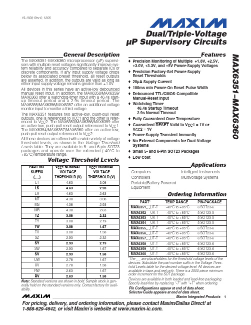
19-1508; Rev 6; 12/05
Dual/Triple-Voltage µP Supervisory Circuits
General Description
The MAX6351–MAX6360 microprocessor (µP) supervisors with multiple reset voltages significantly improve system reliability and accuracy compared to separate ICs or discrete components. If any input supply voltage drops below its associated preset threshold, all reset outputs are asserted. In addition, the outputs are valid as long as either input supply voltage remains greater than +1.0V. All devices in this series have an active-low debounced manual reset input. In addition, the MAX6358/MAX6359/ MAX6360 offer a watchdog-timer input with a 46.4s startup timeout period and a 2.9s timeout period. The MAX6355/MAX6356/MAX6357 offer an additional voltage monitor input to monitor a third voltage. The MAX6351 features two active-low, push-pull reset outputs, one is referenced to VCC1 and the other is referenced to VCC2. The MAX6353/MAX6356/MAX6359 offer an active-low, push-pull reset output referenced to VCC1. The MAX6354/MAX6357/MAX6360 offer an active-low, push-pull reset output referenced to VCC2. All these devices are offered with a wide variety of voltage threshold levels, as shown in the Voltage Threshold Levels table. They are available in 5- and 6-pin SOT23 packages and operate over the extended (-40°C to +85°C) temperature range.
MAX6398中文资料
General DescriptionThe MAX6397/MAX6398 are small, high-voltage overvolt-age protection circuits. These devices disconnect the output load or limit the output voltage during an input overvoltage condition. These devices are ideal for appli-cations that must survive high-voltage transients such as those found in automotive and industrial applications.The MAX6397/MAX6398 monitor the input or output voltages and control an external n-channel MOSFET to isolate or limit the load from overvoltage transient energy.When the monitored input voltage is below the user-adjustable overvoltage threshold, the external n-channel MOSFET is turned on by the GATE output. In this mode,the internal charge pump fully enhances the n-channel MOSFET with a 10V gate-to-source voltage.When the input voltage exceeds the overvoltage thresh-old, the protection can disconnect the load from the input by quickly forcing the GATE output low. In some applications, disconnecting the output from the load is not desirable. In these cases, the protection circuit can be configured to act as a voltage limiter where the GATE output sawtooths to limit the voltage to the load.The MAX6397 also offers an always-on linear regulator that is capable of delivering up to 100mA of output current. This high-voltage linear regulator consumes only 37µA of quiescent current.The regulator is offered with output options of 5V, 3.3V,2.5V, or 1.8V. An open-drain, power-good output (POK)asserts when the regulator output falls below 92.5% or 87.5% of its nominal voltage.The MAX6397/MAX6398 include internal thermal-shut-down protection, disabling the external MOSF ET and linear regulator if the chip reaches overtemperature conditions. The devices operate over a wide 5.5V to 72V supply voltage range, are available in small TDFN packages, and are fully specified from -40°C to +125°C.ApplicationsAutomotive Industrial FireWire ®Notebook Computers Wall Cube Power DevicesFeatures♦5.5V to 72V Wide Supply Voltage Range♦Overvoltage Protection Controllers Allow User to Size External n-Channel MOSFETs ♦Internal Charge-Pump Circuit Ensures MOSFET Gate-to-Source Enhancement for Low R DS(ON)Performance ♦Disconnect or Limit Output from Input During Overvoltage Conditions ♦Adjustable Overvoltage Threshold ♦Thermal-Shutdown Protection♦Always-On, Low-Current (37µA) Linear Regulator Sources Up to 100mA (MAX6397)♦Fully Specified from -40°C to +125°C (T J )♦Small, Thermally Enhanced 3mm x 3mm TDFN PackageMAX6397/MAX6398Overvoltage Protection Switch/LimiterControllers Operate Up to 72V________________________________________________________________Maxim Integrated Products1Pin ConfigurationsOrdering Information19-3668; Rev 3; 1/07For pricing, delivery, and ordering information,please contact Maxim/Dallas Direct!at 1-888-629-4642, or visit Maxim’s website at .Selector Guide and Typical Operating Circuit appear at end of data sheet.FireWire is a registered trademark of Apple Computer, Inc.M A X 6397/M A X 6398Overvoltage Protection Switch/Limiter Controllers Operate Up to 72V 2_______________________________________________________________________________________ABSOLUTE MAXIMUM RATINGSELECTRICAL CHARACTERISTICS(V= 14V; C = 6000pF, C = 4.7µF, T = T = -40°C to +125°C, unless otherwise noted. Typical values are at T = T = +25°C.)(Note 1)Stresses beyond those listed under “Absolute Maximum Ratings” may cause permanent damage to the device. These are stress ratings only, and functional oper-ation of the device at these or any other conditions beyond those indicated in the operational sections of the specifications is not implied. Exposure to absolute maximum rating conditions for extended periods may affect device reliability.(All pins referenced to GND, unless otherwise noted.)IN, GATE, OUT............................................................-0.3V to +80V SHDN ..................................................................-0.3V to (IN + 0.3V)GATE to OUT.................................................................-0.3 to +20V SET, REG, POK...........................................................-0.3V to +12V Maximum Current:IN, REG...............................................................................350mA All Remaining Pins...................................................................50mAContinuous Power Dissipation (T A = +70°C)6-Pin TDFN (derate 18.2mW/°C above +70°C).............1455mW 8-Pin TDFN (derate 18.2mW/°C above +70°C).............1455mW Operating Temperature Range (T A )......................-40°C to +125°C Junction Temperature...........................................................+150°C Storage Temperature Range.................................-65°C to +150°C Lead Temperature................................................................+300°CMAX6397/MAX6398Overvoltage Protection Switch/LimiterControllers Operate Up to 72V_______________________________________________________________________________________3ELECTRICAL CHARACTERISTICS (continued)(V IN = 14V; C GATE = 6000pF, C REG = 4.7µF, T A = T J = -40°C to +125°C, unless otherwise noted. Typical values are at T A = T J = +25°C.)(Note 1)Note 1:Specifications to -40°C are guaranteed by design and not production tested.Note 2:The MAX6397/MAX6398 power up with the external FET in off mode (V GATE = GND). The external FET turns on t START after thedevice is powered up and all input conditions are valid.Note 3:For accurate overtemperature shutdown performance, place the device in close thermal contact with the external MOSFET.Note 4:Dropout voltage is defined as V IN - V REG when V REG is 2% below the value of V REG for V IN = V REG (nominal) + 2V.Note 5:Operations beyond the thermal dissipation limit may permanently damage the device.M A X 6397/M A X 6398Overvoltage Protection Switch/Limiter Controllers Operate Up to 72V 4_______________________________________________________________________________________Typical Operating Characteristics(V IN = 14V, C REG = 4.7µF, I REG = 0, unless otherwise noted.)40608010012014016002010304050607080SUPPLY CURRENT vs. INPUT VOLTAGEINPUT VOLTAGE (V)S U P P L Y C U R R E N T (µA )SUPPLY CURRENT vs. TEMPERATURETEMPERATURE (°C)S U P P L Y C U R R E N T (µA )1007525500-259010011012013014015016017018080-50125405060708090100110120020406080SUPPLY CURRENT vs. INPUT VOLTAGEINPUT VOLTAGE (V)S U P P L Y CU R R E N T (µA )8010090120110130140-502550-25075100125SUPPLY CURRENT vs. TEMPERATURETEMPERATURE (°C)S U P P L YC U R R E N T (µA )20302540354550040206080SHUTDOWN SUPPLY CURRENT vs. INPUT VOLTAGE (MAX6397)INPUT VOLTAGE (V)S U P P L YC U R R E N T (µA )103050700642810121416182020406080SHUTDOWN SUPPLY CURRENTvs. INPUT VOLTAGEINPUT VOLTAGE (V)S U P PL Y C U R R E N T (µA )0642810124121068141618202224GATE-DRIVE VOLTAGE vs. INPUT VOLTAGEINPUT VOLTAGE (V)V G A T E - V O U T (V )4.04.64.44.25.04.85.85.65.45.26.0-50-250255075100125UVLO THRESHOLD vs. TEMPERATUREM A X 6397-98 t o c 08TEMPERATURE (°C)V U V L O (V )SET THRESHOLD vs. TEMPERATUREM A X 6397-98 t o c 09TEMPERATURE (°C)S E T T H R E S H O L D (V )1007525500-251.2041.2081.2121.2161.2201.2241.2281.2321.2361.2401.200-50125MAX6397/MAX6398Overvoltage Protection Switch/LimiterControllers Operate Up to 72V_______________________________________________________________________________________516.016.316.216.116.516.416.916.816.716.617.0-50-25255075100125GATE-TO-OUT CLAMP VOLTAGEvs. TEMPERATUREM A X 6397-98 t o c 10TEMPERATURE (°C)G A T E -T O -O U T C L A M P V O L T A G E (V )00.40.20.80.61.21.01.41.81.62.0040608020100120140160180DROPOUT VOLTAGE vs. REG LOAD CURRENTREG LOAD CURRENT (mA)D R O P O U T V O L T A GE (V )4.905.004.955.105.055.155.20-40-10520-253550658095110125REG OUTPUT VOLTAGEvs. LOAD CURRENT AND TEMPERATURETEMPERATURE (°C)R E G O U T P U T V O L T A G E (V )4.04.64.44.24.85.05.21601204080200240280320360400MAXIMUM REG OUTPUT VOLTAGE vs. LOAD CURRENT AND TEMPERATURELOAD CURRENT (mA)R E G O U T P U T V O L T A G E (V )POWER-SUPPLY REJECTION RATIOvs. FREQUENCYFREQUENCY (Hz)P S R R (d B )1M 100k 10k 1k 100-60-50-40-30-20-100-701010M4ms/divSTARTUP WAVEFORM(R LOAD = 100Ω, C IN = 10µF, C OUT = 10µF)V IN 10V/divMAX6397-98 toc16V GATE 10V/div V OUT 10V/div I OUT200mA/div400µs/divSTARTUP WAVEFORM FROM SHUTDOWN(C IN = 10µF, C OUT = 10µF)V 2V/divV GATE 10V/divV OUT 10V/div I OUT200mA/divR LOAD = 100ΩTypical Operating Characteristics (continued)(V IN = 14V, C REG = 4.7µF, I REG = 0, unless otherwise noted.)GATE-DRIVE VOLTAGE vs. TEMPERATUREM A X 6397-98 t o c 14TEMPERATURE (°C)G A T E -D R I V E V O L T A G E (V )1007525500-2510.45510.46010.46510.47010.47510.48010.48510.49010.49510.50010.450-50125M A X 6397/M A X 6398Overvoltage Protection Switch/Limiter Controllers Operate Up to 72V 6_______________________________________________________________________________________Typical Operating Characteristics (continued)(V IN = 14V, C REG = 4.7µF, I REG = 0, unless otherwise noted.)200µs/divOVERVOLTAGE SWITCH FAULTV IN 20V/divV GATE 20V/div V OUT 20V/div V REG 5V/divV OV = 30V1ms/divVOLTAGE LIMIT FAULTV IN 20V/divV GATE 20V/divV OUT 20V/div V REG 5V/divV OV = 30V400µs/divTRANSIENT RESPONSEV IN 10V/divV REG100mV/divC REG = 10µF I REG = 10mA1ms/divREG LOAD-TRANSIENT RESPONSEV REGAC-COUPLED 500mV/divI REG100mA/divC REG = 10µF1ms/divREGULATOR STARTUP WAVEFORMV IN 10V/divV POK 2V/divV REG 2V/divI REG = 10mA100µs/divREGULATOR POK ASSERTIONV REG 2V/divI REG200mA/div V POK 2V/divI REG = 00V0V0ADetailed Description The MAX6397/MAX6398 are ultra-small, low-current, high-voltage protection circuits for automotive applica-tions that must survive load dump and high-voltage transient conditions. These devices monitor the input/ output voltages and control an external n-channel MOSF ET to isolate the load or to regulate the output voltage from overvoltage transient energy. The con-troller allows system designers to size the external MOSFET to their load current and board size.The MAX6397/MAX6398 drive the MOSF ET’s gate high when the monitored input voltage is below the adjustable overvoltage threshold. An internal charge-pump circuit provides a 5V to 10V gate-to-source drive (see the Typical Operating Characteristics) to ensure low input-to-load voltage drops in normal operating modes. When the input voltage rises above the user-adjusted overvoltage threshold, GATE pulls to OUT, turning off the MOSFET.The MAX6397/MAX6398 are configurable to operate as overvoltage protection switches or as closed-looped volt-age limiters. In overvoltage protection switch mode, theinput voltage is monitored. When an overvoltage condi-tion occurs at IN, GATE pulls low, disconnecting the loadfrom the power source, and then slowly enhances upon removal of the overvoltage condition. In overvoltagelimit mode, the output voltage is monitored and theMAX6397/MAX6398 regulate the source of the external MOSFET at the adjusted overvoltage threshold, allowing devices within the system to continue operating during an overvoltage condition.The MAX6397/MAX6398 undervoltage lockout (UVLO) function disables the devices as long as the input remains below the 5V (typ) UVLO turn-on threshold. TheMAX6397/MAX6398 have an active-low SHDN input toturn off the external MOSFET, disconnecting the load and reducing power consumption. After power is applied and SHDN is driven above its logic-high voltage, there is a100µs delay before GATE enhancement commences.MAX6397/MAX6398Overvoltage Protection Switch/LimiterControllers Operate Up to 72V _______________________________________________________________________________________7M A X 6397/M A X 6398The MAX6397 integrates a high-input-voltage, low-qui-escent-current linear regulator in addition to an over-voltage protector circuit. The linear regulator remains enabled at all times to power low-current “always-on”applications (independent of the state of the external MOSF ET). The regulator is offered with several stan-dard output voltage options (5V, 3.3V, 2.5V, or 1.8V).An open-drain power-good output notifies the system if the regulator output falls to 92.5% or 87.5% of its nomi-nal voltage. The MAX6397’s REG output operates inde-pendently of the SHDN logic input.The MAX6397/MAX6398 include internal thermal-shut-down protection, disabling the external MOSF ET and linear regulator if the chip reaches overtemperature conditions.Linear Regulator (MAX6397 Only)The MAX6397 is available with 5.0V, 3.3V, 2.5V, and 1.8V factory-set output voltages. Each regulator sources up to 100mA and includes a current limit of 230mA. The linear regulator operates in an always-on condition regardless of the SHDN logic. For fully specified operation, V IN must be greater than 6.5V for the MAX6397L/M (5V regulator output). The actual output current may be limited by the operating condition and package power dissipation.Power-OK OutputPOK is an open-drain output that goes low when REG falls to 92.5% or 87.5% (see the Selector Guide ) of its nominal output voltage. To obtain a logic-level output,connect a pullup resistor from POK to REG or another system voltage. Use a resistor in the 100k Ωrange to minimize current consumption. POK provides a valid logic-output level down to V IN = 1.5V.GATE VoltageThe MAX6397/MAX6398 use a high-efficiency charge pump to generate the GATE voltage. Upon V IN exceed-ing the 5V (typ) UVLO threshold, GATE enhances 10V above IN (for V IN ≥14V) with a 75µA pullup current. An overvoltage condition occurs when the voltage at SET pulls above its 1.215V threshold. When the threshold is crossed, GATE falls to OUT within 100ns with a 100mA (typ) pulldown current. The MAX6397/MAX6398 include an internal clamp to OUT that ensures GATE is limited to 18V (max) above OUT to prevent gate-to-source damage to the external FET.The GATE cycle during overvoltage limit and overvolt-age switch modes are quite similar but have distinct characteristics. In overvoltage switch mode (Figure 2a),GATE is enhanced to V IN + 10V while the monitored IN voltage remains below the overvoltage fault threshold (SET < 1.215V). When an overvoltage fault occurs (SET ≥1.215V), GATE is pulled one diode below OUT, turn-ing off the external F ET and disconnecting the load from the input. GATE remains low (FET off) as long as V IN is above the overvoltage fault threshold. As V IN falls back below the overvoltage fault threshold (-5% hys-teresis) GATE is again enhanced to V IN + 10V.In overvoltage limit mode (Figure 2b), GATE is enhanced to V IN + 10V. While the monitored OUT voltage remains below the overvoltage fault threshold (SET < 1.215V).When an overvoltage fault occurs (SET ≥1.215V),GATE is pulled low one diode drop below OUT until OUT drops 5% below the overvoltage fault threshold.GATE is then turned back on until OUT again reaches the overvoltage fault threshold and GATE is again turned off.Overvoltage Protection Switch/Limiter Controllers Operate Up to 72V 8_______________________________________________________________________________________GATE cycles on-off-on-off-on in a sawtooth waveform until OUT remains below the overvoltage fault threshold and GATE remains constantly on (V IN + 10V). The over-voltage limiter’s sawtooth GATE output operates the MOSFET in a switched-linear mode while the input volt-age remains above the overvoltage fault threshold. The sawtooth frequency depends on the load capacitance,load current, and MOSFET turn-on time (GATE charge current and GATE capacitance).GATE goes high when the following startup conditions are met: V IN is above the UVLO threshold, SHDN is high, an overvoltage fault is not present and the device is not in thermal shutdown.Overvoltage MonitoringWhen operating in overvoltage mode, the MAX6397/MAX6398 feedback path (F igure 3) consists of IN,SET’s internal comparator, the internal gate charge pump, and the external n-channel MOSFET resulting in a switch-on/off function. When the programmed over-voltage threshold is tripped, the internal fast compara-tor turns off the external MOSFET, pulling GATE to OUT within t OV and disconnecting the power source from the load. When IN decreases below the adjusted over-voltage threshold, the MAX6397/MAX6398 slowly enhance GATE above OUT, reconnecting the load to the power source.Overvoltage LimiterWhen operating in overvoltage limiter mode, the MAX6397/MAX6398 feedback path (F igure 4) consists of OUT, SET’s internal comparator, the internal gate charge pump and the external n-channel MOSF ET,which results in the external MOSF ET operating as a voltage regulator.During normal operation, GATE is enhanced 10V above OUT. The external MOSFET source voltage is monitored through a resistor-divider between OUT and SET. When OUT rises above the adjusted overvoltage threshold, an internal comparator sinks the charge-pump current, dis-charging the external GATE, regulating OUT at the set overvoltage threshold. OUT remains active during the overvoltage transients and the MOSFET continues to con-duct during the overvoltage event, operating in switched-linear mode.MAX6397/MAX6398Overvoltage Protection Switch/LimiterControllers Operate Up to 72V_______________________________________________________________________________________9V GATE 10V/divV OUT 10V/divV IN 10V/div10ms/divV GATE 10V/divV OUT 10V/divV IN 10V/div4ms/divM A X 6397/M A X 6398As the transient begins decreasing, OUT fall time will depend on the MOSF ET’s GATE charge, the internal charge-pump current, the output load, and the tank capacitor at OUT.For fast-rising transients and very large-sized MOSFETs,add an additional external bypass capacitor from GATE to GND to reduce the effect of the fast-rising voltages at IN. The external capacitor acts as a voltage-divider working against the MOSF ETs’ drain-to-gate capaci-tance. For a 6000pF C gd , a 0.1µF capacitor at GATE will reduce the impact of the fast-rising V IN input.Caution must be exercised when operating the MAX6397/MAX6398 in voltage-limiting mode for long durations. If the V IN is a DC voltage greater than the MOSFET’s maximum gate voltage, the FET will dissipate power continuously. To prevent damage to the external MOSFET, proper heatsinking should be implemented.Applications InformationLoad DumpMost automotive applications run off a multicell, 12V lead-acid battery with a nominal voltage that swings between 9V and 16V (depending on load current,charging status, temperature, battery age, etc.). The battery voltage is distributed throughout the automobile and is locally regulated down to voltages required by the different system modules. Load dump occurs when the alternator is charging the battery and the battery becomes disconnected. Power in the alternator (essen-tially an inductor) flows into the distributed power sys-tem and elevates the voltage seen at each module. The voltage spikes have rise times typically greater than 5ms and decays within several hundred milliseconds but can extend out to 1s or more depending on thecharacteristics of the charging system (F igure 5).These transients are capable of destroying semicon-ductors on the first ‘fault event.’Setting Overvoltage ThresholdsSET provides an accurate means to set the overvoltage level for the MAX6397/MAX6398. Use a resistor-divider to set the desired overvoltage condition (Figure 6). SET has a rising 1.215V threshold with a 5% falling hysteresis.Begin by selecting the total end-to-end resistance,R TOTAL = R1 + R2. Choose R TOTAL to yield a total cur-rent equivalent to a minimum 100 x I SET (SET’s input bias current) at the desired overvoltage threshold.For example:With an overvoltage threshold set to 20V:R TOTAL < 20V/(100 x I SET )where I SET is SET’s 50nA input bias current.R TOTAL < 4M ΩUse the following formula to calculate R2:where V TH is the 1.215V SET rising threshold and V OV is the overvoltage threshold.R2 = 243k Ω, use a 240k Ωstandard resistor.R TOTAL = R2 + R1, where R1 = 3.76M Ω.Use a 3.79M Ωstandard resistor.A lower value for total resistance dissipates morepower but provides slightly better accuracy.Overvoltage Protection Switch/Limiter Controllers Operate Up to 72V 10______________________________________________________________________________________Reverse-Battery ProtectionUse a diode or p-channel MOSF ET to protect the MAX6397/MAX6398 during a reverse-battery insertion (Figures 7a, 7b). Low p-channel MOSFET on-resistance of 30m Ωor less yields a forward-voltage drop of only a few millivolts (versus hundreds of millivolts for a diode,Figure 7a) thus improving efficiency.Connecting a positive battery voltage to the drain of Q1(F igure 7b) produces forward bias in its body diode,which clamps the source voltage one diode drop below the drain voltage. When the source voltage exceeds Q1’s threshold voltage, Q1 turns on. Once the F ET is on, the battery is fully connected to the system and can deliver power to the device and the load.An incorrectly inserted battery reverse-biases the F ET’s body diode. The gate remains at the ground potential.The FET remains off and disconnects the reversed bat-tery from the system. The zener diode and resistor com-bination prevent damage to the p-channel MOSF ET during an overvoltage condition.MAX6397/MAX6398Overvoltage Protection Switch/LimiterControllers Operate Up to 72V______________________________________________________________________________________11M A X 6397/M A X 6398REG Capacitor Selection for StabilityFor stable operation over the full temperature range and with load currents up to 100mA, use ceramic capacitor values greater than 4.7µF. Large output capacitors help reduce noise, improve load-transient response, and power-supply rejection at REG. Note that some ceramic dielectrics exhibit large capacitance and ESR variation with temperature. At lower temperatures, it may be nec-essary to increase capacitance.Under normal conditions, use a 10µF capacitor at rger input capacitor values and lower ESR provide bet-ter supply-noise rejection and line-transient response.Inrush/Slew-Rate ControlInrush current control can be implemented by placing a capacitor at GATE (F igure 8) to slowly ramp up the GATE, thus limiting the inrush current and controlling GATE’s slew rate during initial turn-on. The inrush cur-rent can be approximated using the following formula:where I GATE is GATE’s 75µA sourcing current, I LOAD is the load current at startup, and C OUT is the output capacitor.Input Transients ClampingWhen the external MOSFET is turned off during an over-voltage occurrence, stray inductance in the power path may cause voltage ringing exceeding the MAX6397/MAX6398 absolute maximum input (IN) supply rating.The following techniques are recommended to reduce the effect of transients:•Minimize stray inductance in the power path usingwide traces, and minimize loop area including the power traces and the return ground path.•Add a zener diode or transient voltage suppressor(TVS) rated below the IN absolute maximum rating (Figure 9).Add a resistor in series with IN to limit transient currentgoing into the input for the MAX6398 only.Overvoltage Protection Switch/Limiter Controllers Operate Up to 72V 12______________________________________________________________________________________Figure 8. MAX6397/MAX6398 Controlling GATE Inrush CurrentFigure 9. Protecting the MAX6397/MAX6398 Input from High-Voltage TransientsMOSFET SelectionSelect external MOSF ETs according to the application current level. The MOSF ET’s on-resistance (R DS(ON))should be chosen low enough to have minimum voltage drop at full load to limit the MOSFET power dissipation.Determine the device power rating to accommodate an overvoltage fault when operating the MAX6397/MAX6398 in overvoltage limit mode.During normal operation, the external MOSFETs dissipate little power. The power dissipated in normal operation is:P Q1 = I LOAD 2x R DS(ON).The most power dissipation will occur during a pro-longed overvoltage event when operating the MAX6397/MAX6398 in voltage limiter mode, resulting in high power dissipated in Q1 (F igure 10) where the power dissipated across Q1 is:P Q1= V Q1x I LOADwhere V Q1is the voltage across the MOSF ET’s drain and source.Thermal ShutdownThe MAX6397/MAX6398 thermal-shutdown feature shuts off the linear regulator output, REG, and GATE if it exceeds the maximum allowable thermal dissipation.Thermal shutdown also monitors the PC board tempera-ture of the external nF ET when the devices sit on thesame thermal island. Good thermal contact between the MAX6397/MAX6398 and the external nF ET is essential for the thermal-shutdown feature to operate effectively.Place the nFET as close as possible to OUT.When the junction temperature exceeds T J = +150°C,the thermal sensor signals the shutdown logic, turning off REG’s internal pass transistor and the GATE output,allowing the device to cool. The thermal sensor turns the pass transistor and GATE on again after the IC’s junction temperature cools by 20°C. Thermal-overload protection is designed to protect the MAX6397/MAX6398 and the external MOSFET in the event of cur-rent-limit fault conditions. For continuous operation, do not exceed the absolute maximum junction-tempera-ture rating of T J = +150°C.Thermal ShutdownOvervoltage Limiter ModeWhen operating the MAX6397/MAX6398 in overvoltage limit mode for a prolonged period of time, a thermal shutdown is possible due to device self-heating. The thermal shutdown is dependent on a number of differ-ent factors:•The device’s ambient temperature (T A )•The output capacitor (C OUT )•The output load current (I OUT )•The overvoltage threshold limit (V OV )•The overvoltage waveform period (t OVP )•The power dissipated across the package (P DISS )MAX6397/MAX6398Overvoltage Protection Switch/LimiterControllers Operate Up to 72V______________________________________________________________________________________13M A X 6397/M A X 6398When OUT exceeds the adjusted overvoltage threshold,an internal GATE pulldown current is enabled until OUT drops by 5%. The capacitance at OUT is discharged by the internal current sink and the external OUT load cur-rent. The discharge time (∆t1) is approximately:where V OV is the adjusted overvoltage threshold, I OUT is the external load current and I GATEPD is the GATE’s internal 100mA (typ) pulldown current.When OUT falls 5% below the overvoltage threshold point, the internal current sink is disabled and the MAX6397/MAX6398’s internal charge pump begins recharging the external GATE voltage. The OUT volt-age continues to drop due to the external OUT load current until the MOSF ET gate is recharged. The time needed to recharge GATE and re-enhance the external nFET is approximately:where C ISS is the MOSFET’s input capacitance, V GS(TH)is the MOSFET’s gate-to-source threshold voltage, V F is the internal clamp diode forward voltage (V F = 1.5V typ),and I GATE is the MAX6397/MAX6398 charge-pump cur-rent (75µA typ).During ∆t2, C OUT loses charge through the output load.The voltage across C OUT (∆V2) decreases until the MOSF ET reaches its V GS(TH) threshold and can be approximated using the following formula:Once the MOSFET V GS (TH ) is obtained, the slope of the output voltage rise is determined by the MOSF ET Q G charge through the internal charge pump with respect to the drain potential. The time for the OUT voltage to rise again to the overvoltage threshold can be approxi-mated using the following formula:where ∆V OUT = ( V OV x 0.05) + ∆V2.The total period of the overvoltage waveform can be summed up as follows:t OVP = ∆t1 + ∆t2 + ∆t3The MAX6397/MAX6398 dissipate the most power dur-ing an overvoltage event when I OUT = 0 (C OUT is dis-charged only by the internal current sink). The maximum power dissipation can be approximated using the follow-ing equation:The die temperature (T J ) increase is related to θJC (8.3°C/W and 8.5°C/W for the MAX6397 and MAX6398,respectively) of the package when mounted correctly with a strong thermal contact to the circuit board. The MAX6397/MAX6398 thermal shutdown is governed by the equation:T J = T A + P DISS x (θJC + θCA) < 170°C (typical thermal-shutdown temperature)For the MAX6397, the power dissipation of the internal linear regulator must be added to the overvoltage pro-tection circuit power dissipation to calculate the die temperature. The linear regulator power dissipation is calculated using the following equation:P REG = (V IN – V REG ) (I REG )F or example, using an IRF R3410 100V n-channel MOSF ET, F igure 12 illustrates the junction temperature vs. output capacitor with I OUT = 0, T A = +125°C, V OV < 16V,V F = 1.5V, I GATE = 75mA, and I GATEPD =100mA. Figure 12 shows the relationship between output capacitance versus die temperature for the conditionslisted above.Overvoltage Protection Switch/Limiter Controllers Operate Up to 72V 14______________________________________________________________________________________。
- 1、下载文档前请自行甄别文档内容的完整性,平台不提供额外的编辑、内容补充、找答案等附加服务。
- 2、"仅部分预览"的文档,不可在线预览部分如存在完整性等问题,可反馈申请退款(可完整预览的文档不适用该条件!)。
- 3、如文档侵犯您的权益,请联系客服反馈,我们会尽快为您处理(人工客服工作时间:9:00-18:30)。
General Description The MAX6381–MAX6390 microprocessor (µP) supervisory circuits monitor power-supply voltages from +1.8V to +5.0V while consuming only 3µA of supply current at +1.8V. Whenever V CC falls below the factory-set reset thresholds, the reset output asserts and remains assert-ed for a minimum reset timeout period after V CC rises above the reset threshold. Reset thresholds are available from +1.58V to +4.63V, in approximately 100mV incre-ments. Seven minimum reset timeout delays ranging from 1ms to 1200ms are available.The MAX6381/MAX6384/MAX6387 have a push-pull active-low reset output. The MAX6382/MAX6385/ MAX6388 have a push-pull active-high reset output, and the MAX6383/MAX6386/MAX6389/MAX6390 have an open-drain active-low reset output. The MAX6384/MAX6385/MAX6386 also feature a debounced manual reset input (with internal pullup resistor). The MAX6387/MAX6388/MAX6389 have an auxiliary input for monitoring a second voltage. The MAX6390 offers a manual reset input with a longer V CC reset timeout period (1120ms or 1200ms) and a shorter manual reset timeout (140ms or 150ms).The MAX6381/MAX6382/MAX6383 are available in 3-pin SC70 and6-pinµDFN packages and the MAX6384–MAX6390 are available in 4-pin SC70 andFeatures♦Factory-Set Reset Threshold Voltages Rangingfrom +1.58V to +4.63V in Approximately 100mVIncrements♦±2.5% Reset Threshold Accuracy OverTemperature (-40°C to +125°C)♦Seven Reset Timeout Periods Available: 1ms,20ms, 140ms, 280ms, 560ms, 1120ms,1200ms (min)♦3 Reset Output OptionsActive-Low Push-PullActive-High Push-PullActive-Low Open-Drain♦Reset Output State Guaranteed ValidDown to V CC= 1V♦Manual Reset Input (MAX6384/MAX6385/MAX6386)♦Auxiliary RESET IN(MAX6387/MAX6388/MAX6389)♦V CC Reset Timeout (1120ms or 1200ms)/ManualReset Timeout (140ms or 150ms) (MAX6390)♦Negative-Going V CC Transient Immunity♦Low Power Consumption of 6µA at +3.6Vand 3µA at +1.8V♦Pin Compatible withMAX809/MAX810/MAX803/MAX6326/MAX6327/MAX6328/MAX6346/MAX6347/MAX6348,and MAX6711/MAX6712/MAX6713♦Tiny 3-Pin/4-Pin SC70 and 6-Pin µDFN PackagesMAX6381–MAX6390 SC70/µDFN, Single/Dual Low-Voltage,Low-Power µP Reset Circuits ________________________________________________________________Maxim Integrated Products1Pin Configurations19-1839; Rev 4; 4/07Ordering InformationOrdering Information continued at end of data sheet.Typi cal Operati ng Ci rcui t appears at end of data sheet.Selector Guide appears at end of data sheet.after "XR", "XS", or "LT." Insert reset timeout delay (see ResetTimeout Delay table) after "D" to complete the part number.Sample stock is generally held on standard versions only (seeStandard Versions table). Standard versions have an orderincrement requirement of 2500 pieces. Nonstandard versionshave an order increment requirement of 10,000 pieces.Contact factory for availability of nonstandard versions.+Denotes a lead-free package.For pricing, delivery, and ordering information,please contact Maxim Direct at 1-888-629-4642,or visit Maxim’s website at .ComputersControllersIntelligent InstrumentsCritical µP and µCPower MonitoringPortable/Battery-Powered EquipmentDual Voltage SystemsM A X 6381–M A X 6390SC70/µDFN, Single/Dual Low-Voltage, Low-Power µP Reset CircuitsABSOLUTE MAXIMUM RATINGSELECTRICAL CHARACTERISTICS(V CC = full range, T A = -40°C to +125°C, unless otherwise specified. Typical values are at T A = +25°C.) (Note 1)Stresses beyond those listed under “Absolute Maximum Ratings” may cause permanent damage to the device. These are stress ratings only, and functional operation of the device at these or any other conditions beyond those indicated in the operational sections of the specifications is not implied. Exposure to absolute maximum rating conditions for extended periods may affect device reliability.V CC to GND..........................................................-0.3V to +6.0V RESET Open-Drain Output....................................-0.3V to +6.0V RESET , RESET (push-pull output)..............-0.3V to (V CC + 0.3V)MR , RESET IN.............................................-0.3V to (V CC + 0.3V)Input Current (V CC ).............................................................20mA Output Current (all pins).....................................................20mAContinuous Power Dissipation (T A = +70°C)3-Pin SC70 (derate 2.9mW/°C above +70°C)..............235mW 4-Pin SC70 (derate 3.1mW/°C above +70°C)..............245mW 6-Pin µDFN (derate 2.1mW/°C above +70°C)..........167.7mW Operating Temperature Range .........................-40°C to +125°C Storage Temperature Range.............................-65°C to +150°C Lead Temperature (soldering, 10s).................................+300°CMAX6381–MAX6390SC70/µDFN, Single/Dual Low-Voltage,Low-Power µP Reset Circuits_______________________________________________________________________________________3M A X 6381–M A X 6390SC70/µDFN, Single/Dual Low-Voltage, Low-Power µP Reset Circuits 4______________________________________________________________________________________Typical Operating Characteristics(T A = +25°C, unless otherwise noted.)215436789-40-105-25203550658095110125SUPPLY CURRENT vs. TEMPERATURE(NO LOAD)TEMPERATURE (°C)S U P P L Y C U R R E N T (µA )25292735333137394143-40-105-25203550658095110125POWER-DOWN RESET DELAYvs. TEMPERATURETEMPERATURE (°C)P O W E R -D O W N R E S E T D E L A Y (µs )0.940.980.961.021.001.061.041.08-40-10520-253550658095110125NORMALIZED POWER-UP RESET TIMEOUTvs. TEMPERATUREM A X 6381/90 t o c 03TEMPERATURE (°C)N O R M A L I Z E D R E S E T T I M E O U T P E R I O D0.9900.9851.0150.9950.9901.0001.0051.0101.020-40-10520-253550958011065125M A X 6381/90 t o c 04TEMPERATURE (°C)N O R M A L I Z E D R E S E T TH R E S H O L D NORMALIZED RESET THRESHOLDvs. TEMPERATURE00.40.20.80.61.01.2063912OUTPUT-VOLTAGE LOW vs. SINK CURRENTI SINK (mA)V O L (V )01.00.52.01.52.53.00500750250100012501500OUTPUT-VOLTAGE HIGH vs. SOURCE CURRENTI SOURCE (µA)V O H (V )45001100010010MAXIMUM TRANSIENT DURATION vs. RESET COMPARATOR OVERDRIVE15050350250500200100400300RESET COMPARATOR OVERDRIVE, V TH - V CC (mV)M A X I M U M T R A N S I E N T D U R A T I O N (µs )3.53.93.74.54.34.14.74.95.35.15.5-40-105-25203550658095110125RESET IN TO RESET DELAYvs. TEMPERATUREM A X 6381/90 t o c 08TEMPERATURE (°C)R E S E T I N D E L A Y (µs )MAX6381–MAX6390SC70/µDFN, Single/Dual Low-Voltage,Low-Power µP Reset CircuitsPin DescriptionM A X 6381–M A X 6390SC70/µDFN, Single/Dual Low-Voltage, Low-Power µP Reset Circuits 6_______________________________________________________________________________________Detailed DescriptionRESET OutputA µP reset input starts the µP in a known state. These µP supervisory circuits assert reset to prevent code execution errors during power-up, power-down, or brownout conditions.Reset asserts when V CC is below the reset threshold;once V CC exceeds the reset threshold, an internal timer keeps the reset output asserted for the reset timeout period. After this interval, reset output deasserts. Reset output is guaranteed to be in the correct logic state for V CC ≥1V.Manual Reset Input (MAX6384/MAX6385/MAX6386/MAX6390)Many µP-based products require manual reset capabil-ity, allowing the operator, a test technician, or external logic circuitry to initiate a reset. A logic low on MR asserts reset. Reset remains asserted while MR is low,and for the reset active timeout period (t RP ) after MR returns high. This input has an internal 63k Ωpullup resistor (1.56k Ωfor MAX6390), so it can be left uncon-nected if it is not used. MR can be driven with TTL or CMOS logic levels, or with open-drain/collector outputs.Connect a normally open momentary switch from MR to G ND to create a manual-reset function; external debounce circuitry is not required. If MR is driven from long cables or if the device is used in a noisy environ-ment, connecting a 0.1µF capacitor from MR to G ND provides additional noise immunity.RESET IN Comparator(MAX6387/MAX6388/MAX6389)RESET IN is compared to an internal +1.27V reference.If the voltage at RESET IN is less than 1.27V, reset asserts. Use the RESET IN comparator as a user-adjustable reset detector or as a secondary power-sup-ply monitor by implementing a resistor-divider at RESET IN (shown in Figure 1). Reset asserts when either V CC or RESET IN falls below its respective threshold volt-age. Use the following equation to set the threshold:V INTH = V THRST (R1/R2 + 1)where V THRST = +1.27V. To simplify the resistor selec-tion, choose a value of R2 and calculate R1:R1 = R2 [(V INTH /V THRST ) - 1]Since the input current at RESET IN is 50nA (max),large values can be used for R2 with no significant loss in accuracy.___________Applications InformationNegative-Going V CC TransientsIn addition to issuing a reset to the µP during power-up,power-down, and brownout conditions, the MAX6381–MAX6390 are relatively immune to short dura-tion negative-going V CC transients (glitches).The Typical Operating Characteristics section shows the Maximum Transient Durations vs. Reset Comparator Overdrive, for which the MAX6381–MAX6390 do not generate a reset pulse. This graph was generated usinga negative-going pulse applied to V CC , starting above the actual reset threshold and ending below it by the magnitude indicated (reset comparator overdrive). The graph indicates the typical maximum pulse width a neg-ative-going V CC transient may have without causing a reset pulse to be issued. As the magnitude of the tran-sient increases (goes farther below the reset threshold),the maximum allowable pulse width decreases. A 0.1µF capacitor mounted as close as possible to V CC provides additional transient immunity.Ensuring a Valid RESET Output Down to V CC = 0VThe MAX6381–MAX6390 are guaranteed to operate properly down to V CC = 1V. In applications that require valid reset levels down to V CC = 0V, a pulldown resistor to active-low outputs (push/pull only, Figure 2) and a pullup resistor to active-high outputs (push/pull only)will ensure that the reset line is valid while the reset out-put can no longer sink or source current. This schemedoes not work with the open-drain outputs of the MAX6383/MAX6386/MAX6389/MAX6390. The resistor value used is not critical, but it must be small enough not to load the reset output when V CC is above the reset threshold. For most applications, 100k Ωis ade-quate.MAX6381–MAX6390SC70/µDFN, Single/Dual Low-Voltage,Low-Power µP Reset Circuits_______________________________________________________________________________________7M A X 6381–M A X 6390SC70/µDFN, Single/Dual Low-Voltage, Low-Power µP Reset Circuits 8_______________________________________________________________________________________Selector GuideOrdering Information (continued)Note:Insert reset threshold suffix (see Reset Threshold table)after "XR", "XS", or "LT." Insert reset timeout delay (see Reset Timeout Delay table) after "D" to complete the part number.Sample stock is generally held on standard versions only (see Standard Versions table). Standard versions have an order increment requirement of 2500 pieces. Nonstandard versions have an order increment requirement of 10,000 pieces.Contact factory for availability of nonstandard versions.*MAX6390 is available with D4 or D7 timing only.+Denotes a lead-free package.MAX6381–MAX6390SC70/µDFN, Single/Dual Low-Voltage,Low-Power µP Reset Circuits_______________________________________________________________________________________9Chip InformationTRANSISTOR COUNT: 647PROCESS: BiCMOSPin Configurations (continued)M A X 6381–M A X 6390SC70/µDFN, Single/Dual Low-Voltage, Low-Power µP Reset Circuits 10______________________________________________________________________________________Package Information(The package drawing(s) in this data sheet may not reflect the most current specifications. For the latest package outline information,go to /packages .)MAX6381–MAX6390SC70/µDFN, Single/Dual Low-Voltage,Low-Power µP Reset Circuits______________________________________________________________________________________11Package Information (continued)(The package drawing(s) in this data sheet may not reflect the most current specifications. For the latest package outline information,go to /packages .)M A X 6381–M A X 6390SC70/µDFN, Single/Dual Low-Voltage, Low-Power µP Reset Circuits 12______________________________________________________________________________________Package Information (continued)(The package drawing(s) in this data sheet may not reflect the most current specifications. For the latest package outline information,go to /packages .)SC70/µDFN, Single/Dual Low-Voltage,Low-Power µP Reset CircuitsMaxim cannot assume responsibility for use of any circuitry other than circuitry entirely embodied in a Maxim product. No circuit patent licenses are implied. Maxim reserves the right to change the circuitry and specifications without notice at any time.Maxim Integrated Products, 120 San Gabriel Drive, Sunnyvale, CA 94086 408-737-7600____________________13©2007 Maxim Integrated Productsis a registered trademark of Maxim Integrated Products, Inc.MAX6381–MAX6390Package Information (continued)(The package drawing(s) in this data sheet may not reflect the most current specifications. For the latest package outline information,go to /packages .)Revision HistoryPages changed at Rev 4: Title on all pages, 1, 2, 5,7–13。