74HC165中文资料_数据手册_参数
74HC165 概述
74HC165 概述74HC165是一款高速CMOS器件,74HC165遵循JEDEC标准no.7A。
74HC165引脚兼容低功耗肖特基TTL(LSTTL)系列。
74HC165是8位并行读取或串行输入移位寄存器,可在末级得到互斥的串行输出(Q7和Q7),当并行读取(PL)输入为低时,从D0到D7口输入的并行数据将被异步地读取进寄存器内。
而当PL为高时,数据将从DS输入端串行进入寄存器,在每个时钟脉冲的上升沿向右移动一位(Q0 → Q1 → Q2,等等)。
利用这种特性,只要把Q7输出绑定到下一级的DS输入,即可实现并转串扩展。
74HC165的时钟输入是一个“门控或”结构,允许其中一个输入端作为低有效时钟使能(CE)输入。
CP和CE的引脚分配是独立的并且在必要时,为了布线的方便可以互换。
只有在CP为高时,才允许CE由低转高。
在PL上升沿来临之前,不论是CP还是CE,都应当置高,以防止数据在PL的活动状态发生位移。
74HC165 特性异步8位并行读取同步串行输入兼容JEDEC标准no.7AESD保护HBM EIA/JESD22-A114E超过2000 VMM EIA/JESD22-A115-A超过200 V温度范围-40~+85 ℃-40~+125 ℃74HC165 参数74HC165 基本参数电压 2.0~6.0V驱动电流+/-5.2 mA传输延迟16 ns@5V74HC165 其他特性最高频率56 MHz逻辑电平CMOS功耗考量低功耗或电池供电应用74HC165 封装与引脚SO16, SSOP16, DIP16, TSSOP168 位移位寄存器(并行输入,互补串行输出)简要说明当移位/置入控制端(SH/LD)为低电平时,并行数据(A-H)被置入寄存器,而时钟(CLK,CLK INH)及串行数据(SER)均无关。
当SH/LD为高电平时,并行置数功能被禁止。
CLK和CLK INK在功能上是等价的,可以交换使用。
74HC165功能说明

74HC165功能说明
1.并行输入:74HC165具有8个并行输入引脚(A-H),可以同时读取8个输入信号。
这些输入信号可以是数字信号,也可以是模拟信号。
2.串行输出:74HC165具有串行输出引脚(QH),它可以将输入信号转换为串行输出信号。
输出信号的顺序与输入信号的读取顺序相同。
3.移位操作:74HC165可以通过移位操作来读取并且存储输入信号。
移位操作可以由一个时钟信号(SH/LD)和一个时钟使能信号(CLKINH)来控制。
当时钟使能信号为高电平时,移位操作生效;当时钟使能信号为低电平时,移位操作被禁止。
4.并行加载:除了移位操作之外,74HC165还可以通过并行加载操作来读取并存储输入信号。
并行加载操作可以通过时钟使能引脚(CLKINH)和并行加载引脚(PL)来控制。
当时钟使能引脚为高电平时,同时并行加载引脚为高电平,即可进行并行加载操作。
5.级联操作:多个74HC165芯片可以级联在一起,以扩展输入信号的数量。
级联操作可以通过级联引脚(SERA/B)和级联输出引脚(QH)来实现。
级联引脚可以将一个74HC165的输出连接到另一个74HC165的输入,以实现数据的串行传输。
总结起来,74HC165是一种用于将8个并行输入信号转换为串行输出信号的移位寄存器芯片。
它通过移位操作和并行加载操作来读取并存储输入信号,并且可以通过级联操作扩展输入信号的数量。
这种芯片在数字电路控制和数据采集等应用中非常常见,具有广泛的用途。
74hc165 电平标准
74hc165 电平标准740HC165是一种8位移位寄存器,它常用于电子设备中的数据输入和输出。
在设计和使用电子电路中,了解和理解其电平标准是非常重要的。
首先,让我们来了解一下何为电平标准。
在电子领域中,电平标准用来定义不同电压值所代表的逻辑状态,例如高电平表示1,低电平表示0。
电平标准是为了保证不同设备和电路之间的互操作性以及通信的可靠性。
740HC165的电平标准和逻辑电平定义如下:1.电源电压:740HC165的工作电压范围通常为2V至6V。
这意味着电路在这个电压范围内工作时,可以正常执行其功能。
2.逻辑高电平:对于输入信号而言,当输入电压高于特定阈值电压(通常称为ViH)时,电路将识别为逻辑高电平。
在740HC165中,典型的ViH电平为0.7VCC,其中VCC是电路的电源电压。
也就是说,如果输入电压高于0.7VCC,电路将被视为处于逻辑高电平。
3.逻辑低电平:对于输入信号而言,当输入电压低于特定阈值电压(通常称为ViL)时,电路将识别为逻辑低电平。
在740HC165中,典型的ViL电平为0.3VCC,其中VCC是电路的电源电压。
也就是说,如果输入电压低于0.3VCC,电路将被视为处于逻辑低电平。
4.输出电平:对于输出信号而言,当输出电压高于特定阈值电压(通常称为VOH)时,电路将输出逻辑高电平。
在740HC165中,典型的VOH电平为0.9VCC,其中VCC是电路的电源电压。
相反,当输出电压低于特定阈值电压(通常称为VOL)时,电路将输出逻辑低电平。
在740HC165中,典型的VOL电平为0.1VCC,其中VCC是电路的电源电压。
总结一下,740HC165的电平标准意味着输入电压高于0.7倍的电源电压将被视为逻辑高电平,低于0.3倍的电源电压将被视为逻辑低电平。
对于输出电平而言,高于0.9倍的电源电压将输出逻辑高电平,低于0.1倍的电源电压将输出逻辑低电平。
了解电平标准对于正确设计和使用电子电路至关重要。
74HC165功能说明
74hc165编程说明接触单片机,嵌入式有好长一段时间了,一直想找个机会把自己总结得东西拿出来晒晒太阳(其实没有什么,高手可能早已经了解),在这里我只想分享给与我一样奋斗在单片机一线得广大童鞋么一点小小得甚至卑微得经验.我们都知道通信从大得方面有两种:串行与并行。
串行得最大优点就是占用总线少,但就是传输速率低;并行恰恰相反,占用总线多,传输速率高.市面上有很多这样得芯片,有串入并出得(通俗讲就就是一个一个进,最后一块出来),有并入串出得(相对前者而言)。
具体用哪种类型要根据我们得实际情况。
比如利用单片机显示数码管单纯得显示一个数码管如果仅仅就是为了显示那么动用单片机一个端口(如P0或P1/P2/P3)那没有什么,当然这里我说得数码管就是8段得(如果利用BCD类型16进制数码管那么只需四个即可)就拿51类型得单片机来说,总共32个I/O口,一般如果不就是做太大得工程就是完全够用得,但有些时候您会恨单片机怎么不多长几条“腿",怎么省还就是不够用。
别急集成串行芯片来帮忙哈哈客套话就不多说了言归正传,今天我介绍一下几个在数码管显示或键盘处理中经常用到得移位寄存器芯片,首先登场得就是74HC165:74HC165/74LS165就是典型并入串出芯片,用它来读取外界键盘信息再好不过了,前提我们得了解它,我们先了解其引脚:引出端符号ﻫCLK,CLK INH 时钟输入端(上升沿有效)A-H 并行数据输入端SER 串行数据输入端QH 输出端ﻫQHn 互补输出端SH/LD移位控制/置入控制(低电平有效)真值表时序图其实瞧一个芯片就是如何使用得,不只就是瞧引脚功能,更重要得就是要瞧时序图与真值表,从其中我们可以详细得了解到它就是如何使用得,然后转化成程序代码即可.从上面我们得真值表与时序图中我们要特别注意几个端口得变化,真值表中SH/LD只有在高电平得时候方才有效;CLK,CLK INH只有当其中一个为低电平得时候,另一个时钟才能正确得输入,这就是非常重要得(一般得我们在使用时,可以将其中得一个直接接地,另一个做时钟输入端口使用).但就是我们做事要细心,要一丝不苟,从时序图中我们瞧到SH/LD有一个负脉冲这就是什么缘故呢?在程序设计中如果忽略了此处,那么注定结果就是悲剧得。
(31条消息)74HC165级联电路篇(三)
(31条消息)74HC165级联电路篇(三)
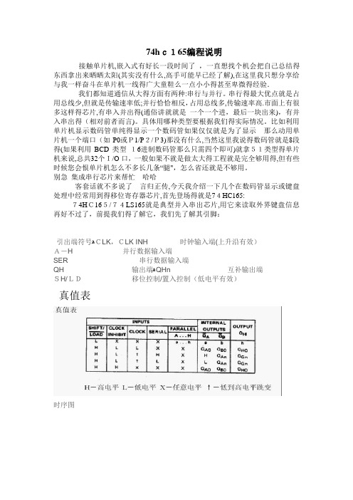
74HC165其实和74HC595一样,也有级联功能,74HC595级联在前面已经整理过,这里说下74hc165的级联。
前面基础篇也讲到74HC165是个并行输入转串行输出的逻辑芯片,该芯片除了串行输出外还有一个串行输入引脚,74HC165的级联功能就使用到这个串行输入引脚,也就是引脚10(DS):
下面就讲下74HC165级联的原理:
从前面的两篇74HC165文章知道,74HC165并行转串行是通过移位寄存器实现的,当PL为低电平时,并行数据(8bit)进入移位寄存器,当PL为高时,进入移位寄存器的数据就从DS引脚进入寄存器,然后在每个时钟的上升沿往输出引脚Q7移一位。
根据这个原理,只要把输出Q7(引脚9)连到下一级74HC165的DS引脚(引脚10)即可实现级联功能,如下图:
最后再以图文并茂的方式总结下74HC165级联后的工作过程,如下图:
74HC165的级联电路就整理到这里,下一篇是级联的编程,总结下如何读取74HC165级联的数据。
ST M74HC165 数据手册

May 2008 Rev 51/21M74HC1658-bit PISO shift registerFeatures■High speed:–t PD = 15 ns (typ.) at V CC = 6 V ■Low power dissipation:–I CC = 4 μA (max.) at T A = 25 °C ■High noise immunity:V NIH = V NIL = 28 % V CC (Min.)■Symmetrical output impedance:|I OH | = I OL = 4 mA (min)■Balanced propagation delays:t PLH ≅ t PHL■Wide operating voltage range:V CC (opr) = 2 V to 6 V■Pin and function compatible with 74 series 165DescriptionThe M74HC165 is a high speed CMOS 8-bit PISO (parallel-in-serial-out) shift registerfabricated with silicon gate C 2MOS technology. This device contains eight clocked master slave RS flip-flops connected as a shift register, with auxiliary gating to provide overridingasynchronous parallel entry. The parallel data enter when the shift/load input is low and can change while shift/load is low, provided that the recommended set-up and hold times areobserved. For clocked operation, shift/load must be high. The two clock inputs perform identically: one can be used as a clock inhibit by applying a high signal, to allow this operation clocking is accomplished through a 2-input nor gate. T o avoid double clocking, however, the inhibit signal should only go high while the clock is high. Otherwise the rising inhibit signal causes the same response as rising clock edge. All inputs are equipped with protection circuits against static discharge and transient excess voltage.Table 1.Device summaryOrder code Package Packaging M74HC165B1R DIP-16T ube M74HC165RM13TR SO-16Tape and reel M74HC165TTRTSSOP16Tape and reelContents M74HC165Contents1Logic symbols and I/O equivalent circuit . . . . . . . . . . . . . . . . . . . . . . . . 32Pin settings . . . . . . . . . . . . . . . . . . . . . . . . . . . . . . . . . . . . . . . . . . . . . . . . 42.1Pin connection . . . . . . . . . . . . . . . . . . . . . . . . . . . . . . . . . . . . . . . . . . . . . . 42.2Pin description . . . . . . . . . . . . . . . . . . . . . . . . . . . . . . . . . . . . . . . . . . . . . . 43Logic states . . . . . . . . . . . . . . . . . . . . . . . . . . . . . . . . . . . . . . . . . . . . . . . . 53.1Truth table . . . . . . . . . . . . . . . . . . . . . . . . . . . . . . . . . . . . . . . . . . . . . . . . . . 53.2Logic diagram . . . . . . . . . . . . . . . . . . . . . . . . . . . . . . . . . . . . . . . . . . . . . . . 53.3Timing chart . . . . . . . . . . . . . . . . . . . . . . . . . . . . . . . . . . . . . . . . . . . . . . . . 64Maximum rating . . . . . . . . . . . . . . . . . . . . . . . . . . . . . . . . . . . . . . . . . . . . . 74.1Recommended operating conditions . . . . . . . . . . . . . . . . . . . . . . . . . . . . . 7 5Electrical characteristics . . . . . . . . . . . . . . . . . . . . . . . . . . . . . . . . . . . . . 8 6Test circuit . . . . . . . . . . . . . . . . . . . . . . . . . . . . . . . . . . . . . . . . . . . . . . . . 11 7Waveforms . . . . . . . . . . . . . . . . . . . . . . . . . . . . . . . . . . . . . . . . . . . . . . . . 12 8Package mechanical data . . . . . . . . . . . . . . . . . . . . . . . . . . . . . . . . . . . . 14 9Revision history . . . . . . . . . . . . . . . . . . . . . . . . . . . . . . . . . . . . . . . . . . . 172/21M74HC165Logic symbols and I/O equivalent circuit 1 Logic symbols and I/O equivalent circuit3/21Pin settings M74HC1654/212 Pin settings2.1 Pin connectionFigure 3.Pin connection (top through view)2.2 Pin descriptionTable 2.Pin descriptionPin numberSymbol Name and function1SHIFT/LOAD Data inputs2CLOCK Clock input (low to high, edge triggered)7QH Complementary output 9QH Serial output 10SI Serial input 11, 12, 13, 14, 3, 4, 5, 6A to H Parallel data inputs 15CLOCK INHClock inhibit 8GND Ground (0V)16V CCPositive supply voltageM74HC165Logic states5/213 Logic states3.1 Truth tableNote:a........h : the level of steady input voltage at inputs a through respectively QAn - QGn : the level of QA - QG, respectively. Before the most recent transition of the clock.3.2 Logic diagramFigure 4.Logic diagramNote:This logic diagram has not to be used to estimate propagation delaysLogic states M74HC1656/213.3 Timing chartFigure 5.Timing chartM74HC165Maximum rating7/214 Maximum ratingStressing the device above the rating listed in the “absolute maximum ratings” table maycause permanent damage to the device. these are stress ratings only and operation of the device at these or any other conditions above those indicated in the operating sections of this specification is not implied. exposure to absolute maximum rating conditions for extended periods may affect device reliability. refer also to the STMicroelectronics sure program and other relevant quality documents.4.1 Recommended operating conditionsTable 4.Absolute maximum ratingsSymbol ParameterValue Unit V CC Supply voltage -0.5 to +7V V I DC input voltage -0.5 to V CC + 0.5V V O DC output voltage -0.5 to V CC + 0.5V I IK DC input diode current ± 20mA I OK DC output diode current ± 20mA I O DC output current ± 25mA I CC or I GND DC V CC or ground current ± 50mA P D Power dissipation 500(1)1.(*) 500mW at 65 °C ; derate to 300mW by 10mW/°C from 65°C to 85°CmW T stg Storage temperature -65 to +150°C T LLead temperature (10 sec)300°CTable 5.Recommended operating conditionsSymsbol ParameterValue Unit V CC Supply voltage 2 to 6V V I Input voltage 0 to V CC V V O Output voltage 0 to V CC V T opOperating temperature-55 to 125°C t r , t fInput rise and fall timeV CC = 2.0V0 to 1000ns V CC = 4.5V 0 to 500ns V CC = 6.0V0 to 400nsElectrical characteristics M74HC1658/215 Electrical characteristicsTable 6.DC specificationsSymbolParameterTest conditionValueUnit V CC(V)T A = 25°C -40 to 85°C -55 to 125°C Min Typ Max Min MaxMin MaxV IHHigh level input voltage2.01.5 1.5 1.5V4.5 3.15 3.15 3.156.0 4.24.24.2V ILLow level input voltage2.00.50.50.5V 4.5 1.35 1.35 1.356.0 1.81.81.8V OHHigh level output voltage2.0I O = -20 μA 1.9 2.0 1.9 1.9V4.5I O =-20 μA 4.4 4.5 4.4 4.46.0I O =-20 μA 5.96.0 5.9 5.94.5I O =-4.0 mA 4.18 4.31 4.13 4.106.0I O =-5.2 mA 5.685.8 5.63 5.60V OLLow level output voltage2.0I O =20 μA 0.00.10.10.1V 4.5I O =20 μA 0.00.10.10.16.0I O =20 μA 0.00.10.10.14.5I O =4.0 mA 0.170.260.330.406.0I O =5.2 mA0.180.260.330.40I I Input leakage current 6.0V I = V CC or GND ± 0.1± 1± 1μA I CCQuiescent supply current6.0V I = V CC or GND44080μAM74HC165Electrical characteristics9/21Table 7.AC electrical characteristics (C L = 50 pF , Input t r = t f = 6ns)SymbolParameterTest conditionValueUnitV CC (V)T A = 25°C -40 to 85°C -55 to 125°C MinTyp Max MinMax MinMax t TLH t THLOutput transition time2.0307595110ns4.581519226.07131619t PLH t PHL Propagation delaytime(CLOCK - QH, QH) 2.0551********ns4.5183038456.015263338t PLH t PHLPropagation delay time(SHIFT/LOAD - QH, QH) 2.065165205250ns4.5213341506.018283543t PLH t PHL Propagation delaytime(H - QH, QH)2.052135170205ns4.5172734416.014232935fMAXMaximum clock frequency2.07.415 6.0 4.8MHz4.5376030246.044713528t W(H) t W(L)Minimum pulse width (CLOCK) 2.024*******ns4.561519226.05131619t W(L)Minimum pulse width(SHIFT/LOAD)2.0327595110ns 4.581519226.07131619t sMinimum set-uptime(PI - S HIFT/LOAD) (SI - CLOCK) (SHIFT/LOAD - CK)2.024*******ns4.561519226.05131619t hMinimum hold time (PI - SHIFT/LOAD)(SI - CLOCK)(SHIFT/LOAD - CK)2.0000ns 4.50006.0000t REMMinimum removal time(CLOCK - CK INH)2.020*******ns 4.551519226.04131619Electrical characteristicsM74HC16510/21Table 8.Capacitive characteristicsSymbolParameterTest conditionValue UnitV CC (V)T A = 25 °C -40 to 85°C -55 to 125°C MinTyp Max MinMax MinMax C IN Input capacitance 5.05101010pF C PDPower dissipation capacitance (1)5.055pF1.C PD is defined as the value of the IC’s internal equivalent capacitance which is calculated from the operating currentconsumption without load. (Refer to Test Circuit). Average operating current can be obtained by the following equation. I CC(opr) = C PD x V CC x f IN + I CCM74HC165Test circuit11/216 Test circuitC L = 50pF or equivalent (includes jig and probe capacitance)R T = Z OUT of pulse generator (typically 50Ω)Waveforms M74HC16512/217 WaveformsFigure 7.Serial mode propagation delay (f = 1MHz; 50% duty cycle)Figure 8.Parallel mode propagation delay (f = 1MHz; 50% duty cycle)M74HC165Waveforms13/21Figure 9.Minimum pulse width (S/L), propagation delay times (f =1MHz; 50% duty cycle)Figure 10.Setup and hold time (PI to S/L)(f = 1MHz; 50% duty cycle)Figure 11.Minimum removal time (CK INH to CK) (f =1MHz; 50% duty cycle)Package mechanical data M74HC165 8 Package mechanical dataIn order to meet environmental requirements, ST offers these devices in ECOPACK®packages. These packages have a Lead-free second level interconnect . The category ofsecond level interconnect is marked on the package and on the inner box label, incompliance with JEDEC Standard JESD97. The maximum ratings related to solderingconditions are also marked on the inner box label. ECOPACK is an ST trademark.ECOPACK specifications are available at: .14/21M74HC165Package mechanical data15/21Package mechanical data M74HC16516/21M74HC165Package mechanical data17/21Package mechanical data M74HC16518/21M74HC165Package mechanical data19/21Revision history M74HC16520/219 Revision historyTable 9.Document revision historyDate RevisionChanges9-Jul-20013Final release.21-Mar-20074The document has been reformatted, updated T able 2: Pindescription on page 426-May-20085Removed: M74HC165M1R order code.Minor changes in the text.Added: SO-16 and TSSOP16 tape and reel specifications.M74HC165Please Read Carefully:Information in this document is provided solely in connection with ST products. STMicroelectronics NV and its subsidiaries (“ST”) reserve the right to make changes, corrections, modifications or improvements, to this document, and the products and services described herein at any time, without notice.All ST products are sold pursuant to ST’s terms and conditions of sale.Purchasers are solely responsible for the choice, selection and use of the ST products and services described herein, and ST assumes no liability whatsoever relating to the choice, selection or use of the ST products and services described herein.No license, express or implied, by estoppel or otherwise, to any intellectual property rights is granted under this document. If any part of this document refers to any third party products or services it shall not be deemed a license grant by ST for the use of such third party products or services, or any intellectual property contained therein or considered as a warranty covering the use in any manner whatsoever of such third party products or services or any intellectual property contained therein.UNLESS OTHERWISE SET FORTH IN ST’S TERMS AND CONDITIONS OF SALE ST DISCLAIMS ANY EXPRESS OR IMPLIED WARRANTY WITH RESPECT TO THE USE AND/OR SALE OF ST PRODUCTS INCLUDING WITHOUT LIMITATION IMPLIED WARRANTIES OF MERCHANTABILITY, FITNESS FOR A PARTICULAR PURPOSE (AND THEIR EQUIVALENTS UNDER THE LAWS OF ANY JURISDICTION), OR INFRINGEMENT OF ANY PATENT, COPYRIGHT OR OTHER INTELLECTUAL PROPERTY RIGHT. UNLESS EXPRESSLY APPROVED IN WRITING BY AN AUTHORIZED ST REPRESENTATIVE, ST PRODUCTS ARE NOT RECOMMENDED, AUTHORIZED OR WARRANTED FOR USE IN MILITARY, AIR CRAFT, SPACE, LIFE SAVING, OR LIFE SUSTAINING APPLICATIONS, NOR IN PRODUCTS OR SYSTEMS WHERE FAILURE OR MALFUNCTION MAY RESULT IN PERSONAL INJURY, DEATH, OR SEVERE PROPERTY OR ENVIRONMENTAL DAMAGE. ST PRODUCTS WHICH ARE NOT SPECIFIED AS "AUTOMOTIVE GRADE" MAY ONLY BE USED IN AUTOMOTIVE APPLICATIONS AT USER’S OWN RISK.Resale of ST products with provisions different from the statements and/or technical features set forth in this document shall immediately void any warranty granted by ST for the ST product or service described herein and shall not create or extend in any manner whatsoever, any liability of ST.ST and the ST logo are trademarks or registered trademarks of ST in various countries.Information in this document supersedes and replaces all information previously supplied.The ST logo is a registered trademark of STMicroelectronics. All other names are the property of their respective owners.© 2008 STMicroelectronics - All rights reservedSTMicroelectronics group of companiesAustralia - Belgium - Brazil - Canada - China - Czech Republic - Finland - France - Germany - Hong Kong - India - Israel - Italy - Japan - Malaysia - Malta - Morocco - Singapore - Spain - Sweden - Switzerland - United Kingdom - United States of America21/21。
74HC165中文资料
Vcc=最小,VIK=-12mA
Vcc = 最 小 VIH = 2V VIL= 0.8V, IOH = -800µA
‘165
最小
最大
-1.5
2.4
单位
V
V V
uA
mA MHz
ns ns ns ns ns ns ns
单位
V V
三毛电子世界
海纳电子资讯网:www.fpga-arm.com 为您提供各种IC中文资料
MHz ns ns ns ns ns
ns
[2]: fmax 最大时钟频率。tPLH输出由低电平到高电平传输延迟时间 tPHL输出由高电平到低 电平传输延迟时间
三毛电子世界
海纳电子资讯网:www.fpga-arm.com 为您提供各种IC中文资料
54/74165
8 位移位寄存器(并行输入,互补串行输出)
简要说明
54/74165 为 8 位移位寄存器,其主要电特性的典型值如下:
型号
fm
PD
54/74165
26MHz 210mW
54/74LS165A
35MHz
90mW
____
参
数[2]
fmax
tPLH tPHL
→ __ _
LD
__
QH, Q H
→ tPLH
CLK
__
QH, Q H
tPHL
→ tPLH H
QH
tPHL
tPLH tPHL
→ __
H QH
测试条件 Vcc =5V,CL=15Pf,RL=400Ω
‘165
最小 24
最大
31
40 24
31 17 36 27 27
AiP74HC165中文使用说明书
-
0
0.1
-
0.1
V
-
0
0.1
-
0.1
V
-
0.15
0.26
-
0.33
V
-
0.16
0.26
-
0.33
V
i-core 输入
漏电流
II
VI =VCC或GND;
VCC=6.0 V
-
-
VI = VCC 或
电源电流
ICC
GND; IO=0A;
-
-
VCC = 6.0 V
输入电容
CI
-
3.5
3.3.2 交流参数 (除非另有规定,CL = 50 pF)
单位 V V V
°C
参数名称 高电平 输入电压 低电平 输入电压
高电平 输出电压
符号 VIH VIL
VOH
测试条件
VCC=2.0V VCC=4.5V VCC=6.0V VCC=2.0V VCC=4.5V VCC=6.0V VI=VIH 或 VIL IO = -20uA; VCC = 2.0 V IO = -20uA; VCC = 4.5 V IO = -20uA; VCC = 6.0 V
3.3、电气特性 3.3.1 直流参数
Ptot
Tamb Tstg TL
-40~+85°C
10 秒
符号
VCC Vቤተ መጻሕፍቲ ባይዱ VO Tamb
最小 2.0 0 0 -40
DIP16
SOP16 SSOP16
DIP SOP
典型 5.0 -
750
500
mW
500
-40~+85
第4节:“鸿哥三宝”之74HC165(按键扫描篇)
第4节:“鸿哥三宝”之74HC165(按键扫描篇)本帖最后由 jianhong_wu 于 2013-1-30 16:19 编辑第四节:“鸿哥三宝”之74HC165(按键扫描篇)(1)开场白:这节将要跟大家介绍一下鸿哥的“三宝”,它们分别是74HC165,74HC595,ULN2003A.之所以它们在我心中的地位那么高,是因为很多工控小项目经常用到它。
74HC165使我们从此不再为单片机的输入口不足而烦恼,我们用3根IO口就可以检测100多路的输入信号。
74HC595使我们从此不再为单片机的输出口不足而烦恼,我们用4根IO口就可以驱动100多个继电器或者LED。
而ULN2003A则大大简化了我们的三极管驱动电路,一个芯片就集成了7个三极管,它有500mA的驱动能力,内部自带续流二极管,用来驱动继电器的时候,二极管也省了。
74HC165对静电很敏感,很脆弱,在通电的情况,绝对不要用手摸到他的引脚,我曾经用非绝缘的镊子来短接其输入口,烧坏了很多个,因此对于74HC165我们要懂得怜香惜玉,小心呵护。
总之,“鸿哥三宝”实乃电子工程师居家旅行之必备良药。
(2)功能需求:每按一个按键,蜂鸣器就响一次。
(3)硬件原理:(a)把两个74HC165联级起来,就可以达到用3根IO口来检测16个按键的目的。
此电路的本质是并入串出的原理。
具体的电路读者只要下载芯片资料一看就明。
还是那句话,按键那里记得接20K左右的上拉电阻。
(b)用1个IO经过8050三极管来驱动有源蜂鸣器,有源蜂鸣器通电就一直响,断电就停止。
(4)源码适合的单片机:PIC18f4520,晶振为22.1184MHz(5)源代码讲解如下:#include //包含芯片相关头文件//补充说明:吴坚鸿程序风格是这样的,凡是输出IO后缀都是_dr,凡是输入的//IO后缀都//是_sr#define beep_dr LATA2 //蜂鸣器输出# define hc165_cp_dr LATA0 //74hc165的3根驱动IO之一# define hc165_pl_dr LATA1 //74hc165的3根驱动IO之一# define hc165_q7_sr RE0 //74hc165的3根驱动IO之一//补充说明:吴坚鸿程序风格是这样的,凡是做延时计数阀值的常量//前缀都用cnt_表示。
74HC165笔记
1、芯片简介
74HC165/74HCT165是一个8位串行或并行输入,串行输出的移位寄存器。
PL为低电平并行,PL为高时就是串行。
具有一个串行输入(DS引脚),8个并行数据输入(D0到D7)和两个互补串行输出的功能。
芯片框图如下:
2、管脚定义
符号引脚描述
PL 1 异步并联负载输入(低电平)
CP 2 时钟输入(低至高沿触发)
Q7 7 上一阶段的互补输出
GND 8 ground (0 V)
Q7 9 最后阶段的串行输出
DS 10 串行数据输入
D0toD7 11, 12, 13, 14, 3, 4, 5, 6 并行数据输入(也称为Dn)
CE 15 钟使能输入(活动低电平)
VCC 16 3.3V
2、芯片真值表
第一个红框是并行加载数据的,只要PL为低电平即可;
第二个蓝框是串行移位,此时要求PL为高电平,CE为低电平,Q0~Q6在CP每来一个上升沿时依次往Q7移位;
第三个紫框是保持当前状态输出。
芯片时序图
当PL引脚为低时,D0-D7端的数据进入移位寄存器。
当PL引脚为高时,数据从DS引脚串行进入寄存器。
当CE引脚为低时,使能时钟,数据在时钟CP上升时数据进行移位。
当CE引脚为高时,失能时钟,时钟输入无效。
总结几个步骤:
1、引脚1(PL)为低电平,获取并行数据输入,数据移入移位寄存器;
2、将引脚1置为高电平,停止并行数据输入;
3、引脚15(OE)为低电平,使能时钟输入;
4、时钟CP每产生一个上升沿,移位寄存器中的数据从高位(Q6)到低位(Q0)依次移出到Q7。
- 1、下载文档前请自行甄别文档内容的完整性,平台不提供额外的编辑、内容补充、找答案等附加服务。
- 2、"仅部分预览"的文档,不可在线预览部分如存在完整性等问题,可反馈申请退款(可完整预览的文档不适用该条件!)。
- 3、如文档侵犯您的权益,请联系客服反馈,我们会尽快为您处理(人工客服工作时间:9:00-18:30)。
4 4
PQD
74HC_HCT165
Product data sheet
All information provided in this document is subject to legal disclaimers.
Rev. 4 — 28 December 2015
© Nexperia B.V. 2017. All rights reserved
SOT338-1
Nexperia
74HC165; 74HCT165
8-bit parallel-in/serial out shift register
Table 1. Ordering information …continued
Type number Package
Temperature range Name
Table 4. Limiting values In accordance with the Absolute Maximum Rating System (IEC 60134). Voltages are referenced to GND (ground = 0 V)
Rev. 4 — 28 December 2015
© Nexperia B.V. 2017. All rights reserved
4 of 21
Nexperia
74HC165; 74HCT165
8-bit parallel-in/serial out shift register
8. Limiting values
Description
Version
plastic small outline package; 16 leads; body width 3.9 mm SOT109-1
plastic shrink small outline package; 16 leads; body width 5.3 mm
Description
74HC165PW 40 C to +125 C TSSOP16 plastic thin shrink small outline package; 16 leads; body
74HCT165PW
width 4.4 mm
74HC165BQ 40 C to +125 C 74HCT165BQ
h
X
H
q0 to q5 q6
q6
hold “do nothing” H
H
X
X
X
q0
q1 to q6 q7
q7
H
X
H
X
X
q0
q1 to q6 q7
q7
[1] H = HIGH voltage level; h = HIGH voltage level one set-up time prior to the LOW-to-HIGH clock transition; L = LOW voltage level; l = LOW voltage level one set-up time prior to the LOW-to-HIGH clock transition; q = state of the referenced output one set-up time prior to the LOW-to-HIGH clock transition; X = don’t care; = LOW-to-HIGH clock transition.
Fig 5. Pin configuration (DHVQFN16)
6.2 Pin description
Table 2. Symbol PL CP Q7 GND Q7 DS D0 to D7 CE VCC
Pin description Pin 1 2 7 8 9 10 11, 12, 13, 14, 3, 4, 5, 6 15 16
PQD
Fig 2. IEC logic symbol
3/
' ' ' ' ' ' ' '
Fig 3. Functional diagram
'6
&3 &(
%,76+,)75(*,67(5 3$5$//(/,16(5,$/287
2 of 21
Nexperia
74HC165; 74HCT165
8-bit parallel-in/serial out shift register
6. Pinning information
6.1 Pinning
+& +&7
3/ &3 ' ' ' ' 4 *1'
2. Features and benefits
Asynchronous 8-bit parallel load Synchronous serial input Complies with JEDEC standard no. 7A Input levels:
For 74HC165: CMOS level For 74HCT165: TTL level ESD protection: HBM JESD22-A114F exceeds 2000 V MM JESD22-A115-A exceeds 200 V Specified from 40 C to +85 C and from 40 C to +125 C
74HC_HCT165
Product data sheet
All information provided in this document is subject to legal disclaimers.
Rev. 4 — 28 December 2015
© Nexperia B.V. 2017. All rights reserved
3. Applications
Parallel-to-serial data conversion
4. Ordering information
Table 1. Ordering information Type number Package
Temperature range Name 74HC165D 40 C to +125 C SO16 74HCT165D 74HC165DB 40 C to +125 C SSOP16 74HCT165DB
9&& &( ' ' ' ' '6 4 DDK
Fig 4. Pin configuration (SO16 and (T)SSOP16)
WHUPLQDO LQGH[DUHD
+& +&7
3/ 9&&
Outputs
PL
CE
CP
DS
D0 to D7 Q0
Q1 to Q6 Q7
Q7
parallel load
L
X
X
X
L
L
L to L L
H
L
X
பைடு நூலகம்
X
X
H
H
H to H H
L
serial shift
H
L
l
X
L
q0 to q5 q6
q6
H
L
h
X
H
q0 to q5 q6
q6
H
L
l
X
L
q0 to q5 q6
q6
H
L
5. Functional diagram
'6 '
'
'
'
'
'
'
4
'
4
3/
&3 &(
PQD
Fig 1. Logic symbol
65*
&>/2$'@
*>6+,)7@
&
' ' '
Description asynchronous parallel load input (active LOW) clock input (LOW-to-HIGH edge-triggered) complementary output from the last stage ground (0 V) serial output from the last stage serial data input parallel data inputs (also referred to as Dn) clock enable input (active LOW) positive supply voltage
&3 &( '6 3/ ' ' ' ' ' ' '
'
4
4
Fig 6. Timing diagram
LQKLELW ORDG
VHULDOVKLIW
PQD
74HC_HCT165
Product data sheet
All information provided in this document is subject to legal disclaimers.