FQPF13N50C中文资料
FQP13N50C中文资料
--
--
IGSSF IGSSR
Gate-Body Leakage Current, Forward VGS = 30 V, VDS = 0 V Gate-Body Leakage Current, Reverse VGS = -30 V, VDS = 0 V
--
--
--
--
--
--
1 10 100 -100
FQP13N50C FQPF13N50C
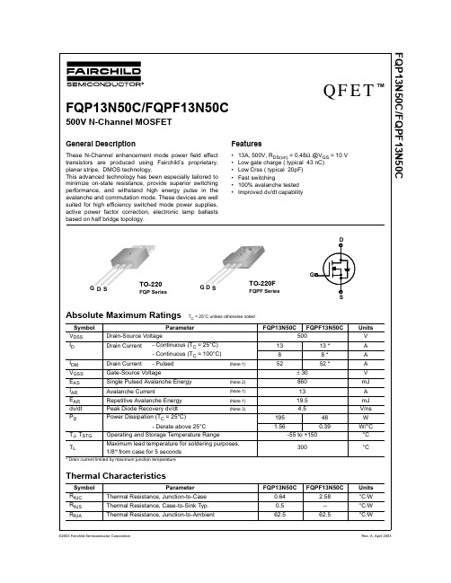
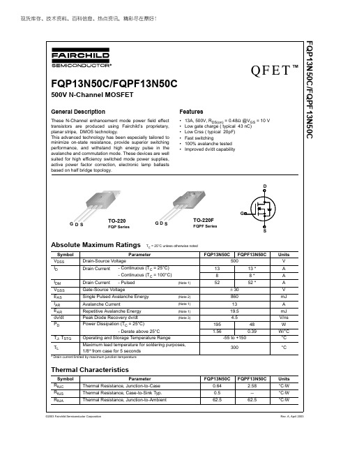
500
13
13 *
8
8*
52
52 *
± 30
860
13
19.5
4.5
195
48
1.56
0.39
-55 to +150
300
Units V A A A V mJ A mJ
V/ns W
W/°C °C
°C
Thermal Characteristics
Symbol RθJC RθJS RθJA
2.0 --
4.0
V
VGS = 10 V, ID = 6.5 A
-- 0.39 0.48
Ω
VDS = 40 V, ID = 6.5 A
(Note 4) --
15
--
S
Dynamic Characteristics
Ciss
Input Capacitance
Coss
Output Capacitance
Crss
Drain Current - Continuous (TC = 25°C)
- Continuous (TC = 100°C)
IDM
Drain Current - Pulsed
FQPF13N50CF中文资料
Notes:1. Repetitive Rating: Pulse width limited by maximum junction temperature2. L = 5.6mH, I AS = 13A, V DD = 50V, R G = 25 Ω, Starting T J = 25°C3. I SD ≤ 13A, di/dt ≤ 200A/µs, V DD ≤ BV DSS, Starting T J = 25°C4. Pulse Test: Pulse width ≤ 300µs, Duty Cycle ≤ 2%5. Essentially Independent of Operating Temperature Typical Characteristicsf = 1.0MHzC oss Output Capacitance--180235pF C rss Reverse Transfer Capacitance --2025pF Switching Characteristicst d(on)Turn-On Delay Time V DD = 250V, I D = 13A R G = 25Ω(Note 4, 5)--2560ns t r Turn-On Rise Time --100210ns t d(off)Turn-Off Delay Time --130270ns t f Turn-Off Fall Time --100210ns Q g Total Gate Charge V DS = 400V, I D = 13A V GS = 10V(Note 4, 5)--4356nC Q gs Gate-Source Charge --7.5--nC Q gd Gate-Drain Charge--18.5--nC Drain-Source Diode Characteristics and Maximum RatingsI S Maximum Continuous Drain-Source Diode Forward Current ----13A I SM Maximum Pulsed Drain-Source Diode Forward Current ----52A V SD Drain-Source Diode Forward Voltage V GS = 0V, I S = 13A---- 1.4V t rr Reverse Recovery Time V GS = 0V, I S = 13AdI F /dt =100A/µs (Note 4)--100160ns Q rrReverse Recovery Charge--0.35--µCUnclamped Inductive Switching Test Circuit & WaveformsLIFE SUPPORT POLICYFAIRCHILD’S PRODUCTS ARE NOT AUTHORIZED FOR USE AS CRITICAL COMPONENTS IN LIFE SUPPORT DEVICES OR SYSTEMS WITHOUT THE EXPRESS WRITTEN APPROVAL OF FAIRCHILD SEMICONDUCTOR CORPORATION.As used herein:1. Life support devices or systems are devices or systems which, (a) are intended for surgical implant into the body, or (b) support or sustain life, or (c) whose failure to perform when properly used in accordance with instructions for use provided in the labeling, can be reasonably expected to result in significant injury to the user.2. A critical component is any component of a life support device or system whose failure to perform can be reasonably expected to cause the failure of the life support device or system, or to affect its safety or effectiveness.PRODUCT STATUS DEFINITIONSDefinition of TermsDatasheet Identification Product Status DefinitionAdvance Information Formative or InDesign This datasheet contains the design specifications for product development. Specifications may change in any manner without notice.Preliminary First Production This datasheet contains preliminary data, andsupplementary data will be published at a later date.Fairchild Semiconductor reserves the right to makechanges at any time without notice in order to improvedesign.No Identification Needed Full Production This datasheet contains final specifications. FairchildSemiconductor reserves the right to make changes atany time without notice in order to improve design. Obsolete Not In Production This datasheet contains specifications on a productthat has been discontinued by Fairchild semiconductor.The datasheet is printed for reference information only.Rev. I19。
FAIRCHILD FQP13N50C FQPF13N50C 说明书
现货库存、技术资料、百科信息、热点资讯,精彩尽在鼎好!FQP13N50C/FQPF13N50CNotes:1. Repetitive Rating : Pulse width limited by maximum junction temperature2. L =6.0 mH, I AS = 13A, V DD = 50V, R G = 25 Ω, Starting T J = 25°C3. I SD ≤ 13A, di/dt ≤ 200A/µs, V DD ≤ BV DSS, Starting T J = 25°C4. Pulse Test : Pulse width ≤ 300µs, Duty cycle ≤ 2%5. Essentially independent of operating temperatureV GS(th)Gate Threshold Voltage V DS = V GS , I D = 250 µA 2.0-- 4.0V R DS(on)Static Drain-Source On-ResistanceV GS = 10 V, I D = 6.5 A--0.390.48Ωg FSForward TransconductanceV DS = 40 V, I D = 6.5 A (Note 4)--15--SDynamic CharacteristicsC iss Input Capacitance V DS = 25 V, V GS = 0 V, f = 1.0 MHz--15802055pF C oss Output Capacitance--180235pF C rssReverse Transfer Capacitance--2025pFSwitching Characteristicst d(on)Turn-On Delay Time V DD = 250 V, I D = 13 A,R G = 25 Ω(Note 4, 5)--2560ns t r Turn-On Rise Time --100210ns t d(off)Turn-Off Delay Time --130270ns t f Turn-Off Fall Time --100210ns Q g Total Gate Charge V DS = 400 V, I D = 13 A,V GS = 10 V(Note 4, 5)--4356nC Q gs Gate-Source Charge --7.5--nC Q gdGate-Drain Charge--18.5--nCDrain-Source Diode Characteristics and Maximum RatingsI S Maximum Continuous Drain-Source Diode Forward Current ----13A I SM Maximum Pulsed Drain-Source Diode Forward Current----52A V SD Drain-Source Diode Forward Voltage V GS = 0 V, I S = 13 A ---- 1.4V t rr Reverse Recovery Time V GS = 0 V, I S = 13 A,dI F / dt = 100 A/µs (Note 4)--410--ns Q rrReverse Recovery Charge-- 4.5--µCDISCLAIMERFAIRCHILD SEMICONDUCTOR RESERVES THE RIGHT TO MAKE CHANGES WITHOUT FURTHER NOTICE TO ANY PRODUCTS HEREIN TO IMPROVE RELIABILITY, FUNCTION OR DESIGN. FAIRCHILD DOES NOT ASSUME ANY LIABILITY ARISING OUT OF THE APPLICATION OR USE OF ANY PRODUCT OR CIRCUIT DESCRIBED HEREIN;NEITHER DOES IT CONVEY ANY LICENSE UNDER ITS PATENT RIGHTS, NOR THE RIGHTS OF OTHERS.LIFE SUPPORT POLICYFAIRCHILD’S PRODUCTS ARE NOT AUTHORIZED FOR USE AS CRITICAL COMPONENTS IN LIFE SUPPORT DEVICES OR SYSTEMS WITHOUT THE EXPRESS WRITTEN APPROVAL OF FAIRCHILD SEMICONDUCTOR CORPORATION.As used herein:1. Life support devices or systems are devices or systems which, (a) are intended for surgical implant into the body,or (b) support or sustain life, or (c) whose failure to perform when properly used in accordance with instructions for use provided in the labeling, can be reasonably expected to result in significant injury to the user.2. A critical component is any component of a life support device or system whose failure to perform can be reasonably expected to cause the failure of the life support device or system, or to affect its safety or effectiveness.PRODUCT STATUS DEFINITIONS Definition of TermsDatasheet Identification Product Status DefinitionAdvance InformationFormative or In Design This datasheet contains the design specifications for product development. Specifications may change in any manner without notice.PreliminaryFirst ProductionThis datasheet contains preliminary data, andsupplementary data will be published at a later date.Fairchild Semiconductor reserves the right to make changes at any time without notice in order to improve design.No Identification Needed Full ProductionThis datasheet contains final specifications. Fairchild Semiconductor reserves the right to make changes at any time without notice in order to improve design.Obsolete Not In ProductionThis datasheet contains specifications on a product that has been discontinued by Fairchild semiconductor.The datasheet is printed for reference information only.TRADEMARKSThe following are registered and unregistered trademarks Fairchild Semiconductor owns or is authorized to use and is not intended to be an exhaustive list of all such trademarks.FACT™FACT Quiet series™FAST ®FASTr™FRFET™GlobalOptoisolator™GTO™HiSeC™I 2C™ImpliedDisconnect™ISOPLANAR™LittleFET™MicroFET™MicroPak™MICROWIRE™MSX™MSXPro™OCX™OCXPro™OPTOLOGIC ®OPTOPLANAR™PACMAN™POP™Power247™PowerTrench ®QFET™QS™QT Optoelectronics™Quiet Series™RapidConfigure™RapidConnect™SILENT SWITCHER ®SMART START™SPM™Stealth™SuperSOT™-3SuperSOT™-6SuperSOT™-8SyncFET™TinyLogic ®TruTranslation™UHC™UltraFET ®VCX™ACEx™ActiveArray™Bottomless™CoolFET™CROSSVOLT ™DOME™EcoSPARK™E 2CMOS™EnSigna™Across the board. Around the world.™The Power Franchise™Programmable Active Droop™。
逆变器用到的IC
KA5H0165RN 原装正品 06年份 FSC 4000 现货
FSDM0265RNB 原装正品 06年份 FSC 40000 香港现货
FSDL0165RN 原装正品 06年份 FSC 9000 香港现货
FSDH321 原装正品 06年份 FSC 12000 香港现货
STP10NK60 原装正品 04年份 ST 10000 现货
IRF640B 原装正品 04年份 FSC 3800 现货
IRF630B 原装正品 06年份 FSC 2000 现货
FDP2532 原装正品 06年份 FSC 4200 现货
FQP50N06 原装正品 07年份 FSC 20000 现货
SSH70N10A 原装正品 07年份 FSC 480 香港现货
FQA160N08 原装正品 06年份 FSC 1300 现货
FQA40N25 原装正品 05年份 FSC 340 现货
FQA16N50 原装正品 04年份 FSC 2600 现货
FQPF10N60C 原装正品 07年份 FSC 6000 现货
FQPF12N60C 原装正品 07年份 FSC 550 现货
KA5L0380RYDTU 原装正品 07年份 FSC 10000 香港现货
FQPF8N60C 原装正品 07年份 FSC 20000 香港现货
2SK2645 原装正品 06年份 FUJI 5400 现货
2SK2765 原装正品 06年份 FUJI 2500 现货
FQA90N15 原装正品 06年份 FSC 500 现货
IRFP460C 原装正品 06.07年份 FSC 5600 香港现货
FQPF2N60C资料

100
150℃ 25℃
※ Notes :
1. 2.
2V5GS0μ=s0VPulse
Test
10-1
0.2
0.4
0.6
0.8
1.0
1.2
1.4
VSD, Source-Drain voltage [V]
Figure 4. Body Diode Forward Voltage Variation with Source Current and Temperature
VGS = 0 V, IS = 2 A,
-- 230
--
ns
Qrr
Reverse Recovery Charge
dIF / dt = 100 A/µs
(Note 4) --
1.0
--
µC
Notes:
1. Repetitive Rating : Pulse width limited by maximum junction temperature
Parameter Thermal Resistance, Junction-to-Case Thermal Resistance, Case-to-Sink Typ. Thermal Resistance, Junction-to-Ambient
FQP2N60C 2.32 0.5 62.5
FQPF2N60C 5.5 -62.5
元器件交易网
FQP2N60C/FQPF2N60C
FQP2N60C/FQPF2N60C
600V N-Channel MOSFET
QFET TM
General Description
These N-Channel enhancement mode power field effect transistors are produced using Fairchild’s proprietary, planar stripe, DMOS technology. This advanced technology has been especially tailored to minimize on-state resistance, provide superior switching performance, and withstand high energy pulse in the avalanche and commutation mode. These devices are well suited for high efficiency switched mode power supplies, active power factor correction, electronic lamp ballasts based on half bridge topology.
13n50场效应管参数

13n50场效应管参数13N50场效应管是一种常见的功率场效应管,具有很高的导通能力和电源效率。
以下是对13N50场效应管参数的详细介绍。
1. 器件结构与特征13N50场效应管由四个主要部分组成:栅、漏极、源极和衬底。
源极和漏极之间形成了一个N型道。
当栅极的电压变化时,栅电场的影响将使N型道中的电子浓度发生变化,从而影响导通区域的电阻。
13N50场效应管的主要特征是其低漏电流和快速开关速度。
由于其低漏电流,它具有极高的电源效率。
13N50场效应管还具有较低的开关损失和较少的热管理需求。
2. 主要参数- 额定电压(VDS):13N50场效应管的额定电压为500V。
- 额定电流(ID):13N50场效应管的额定电流为13A。
- 静态电阻(RDS(on)):13N50场效应管的静态电阻为0.55Ω。
- 最大功耗(PD):13N50场效应管的最大功耗为240W。
- 工作温度范围:13N50场效应管的工作温度范围为-55℃至150℃。
- 开关速度:13N50场效应管的开关速度较快,一般在几纳秒到几十纳秒之间。
3. 应用领域13N50场效应管可以在各种应用领域中使用,包括驱动电机、DC-DC转换器和照明等。
在电机驱动应用中,13N50场效应管可用于控制电机的转速和转向。
它们还可以用于电源开关,特别是在变换器电路中。
在DC-DC转换器中,13N50场效应管可用于控制输出电压。
这些转换器可以将一个电压转换为更高或更低的电压。
它们可以将12伏特的电压升高到24伏特,以使其适合某些应用程序。
在照明应用中,13N50场效应管可用于控制LED照明系统的电流和亮度。
这些场效应管还可以用于LED屏幕和平板电脑背光等其他应用领域。
随着各种电子设备的需求不断增加,13N50场效应管已经成为许多应用领域中的理想选择之一,其特有的性能和参数使其具有广泛的适用性和较广的应用场景。
13N50场效应管广泛应用于各种电子设备中,在工业、通讯、航空航天等领域都有着广泛的应用。
FAIRCHILD FQPF9N30 数据手册

现货库存、技术资料、百科信息、热点资讯,精彩尽在鼎好!F Q P F 9N 30FQPF9N30300V N-Channel MOSFETGeneral DescriptionThese N-Channel enhancement mode power field effect transistors are produced using Fairchild’s proprietary,planar stripe, DMOS technology.This advanced technology has been especially tailored to minimize on-state resistance, provide superior switching performance, and withstand high energy pulse in the avalanche and commutation mode. These devices are well suited for high efficiency switching DC/DC converters,switch mode power supply.TO-220FG SDFQPF9N30(Note 4)(Note 4, 5)(Note 4, 5) (Note 4)Electrical Characteristics T C= 25°C unless otherwise notedNotes:1. Repetitive Rating : Pulse width limited by maximum junction temperature2. L = 19.4mH, I AS = 6.0A, V DD = 50V, R G = 25 Ω, Starting T J = 25°C3. I SD ≤9.0A, di/dt ≤ 200A/µs, V DD ≤ BV DSS, Starting T J = 25°C4. Pulse Test : Pulse width ≤300µs, Duty cycle ≤2%5. Essentially independent of operating temperatureSymbol Parameter Test Conditions Min Typ Max UnitsOff CharacteristicsBV DSS Drain-Source Breakdown Voltage V GS = 0 V, I D = 250 µA300----V ∆BV DSS / ∆T J Breakdown Voltage Temperature CoefficientI D = 250 µA, Referenced to 25°C --0.28--V/°C I DSS Zero Gate Voltage Drain Current V DS = 300 V, V GS = 0 V ----1µA V DS = 240 V, T C = 125°C ----10µA I GSSF Gate-Body Leakage Current, Forward V GS = 30 V, V DS = 0 V ----100nA I GSSRGate-Body Leakage Current, ReverseV GS = -30 V, V DS = 0 V-----100nAOn CharacteristicsV GS(th)Gate Threshold Voltage V DS = V GS , I D = 250 µA 3.0-- 5.0V R DS(on)Static Drain-Source On-ResistanceV GS = 10 V, I D = 3.0 A --0.350.45Ωg FSForward TransconductanceV DS = 50 V, I D = 3.0 A--4.2--SDynamic CharacteristicsC iss Input Capacitance V DS = 25 V, V GS = 0 V, f = 1.0 MHz--570740pF C oss Output Capacitance--120155pF C rssReverse Transfer Capacitance--1620pFSwitching Characteristicst d(on)Turn-On Delay Time V DD = 150 V, I D = 9.0 A,R G = 25 Ω--1640ns t r Turn-On Rise Time --120250ns t d(off)Turn-Off Delay Time --2765ns t f Turn-Off Fall Time --48110ns Q g Total Gate Charge V DS = 240 V, I D = 9.0 A,V GS = 10 V--1722nC Q gs Gate-Source Charge -- 3.9--nC Q gdGate-Drain Charge--9.2--nCDrain-Source Diode Characteristics and Maximum RatingsI S Maximum Continuous Drain-Source Diode Forward Current ---- 6.0A I SM Maximum Pulsed Drain-Source Diode Forward Current----24A V SD Drain-Source Diode Forward Voltage V GS = 0 V, I S = 6.0 A ---- 1.5V t rr Reverse Recovery Time V GS = 0 V, I S = 9.0 A,dI F / dt = 100 A/µs--170--ns Q rrReverse Recovery Charge-- 1.4--µCF Q P F 9N 30FQPF9N30F Q P F 9N 30FQPF9N30F Q P F 9N 30TRADEMARKSThe following are registered and unregistered trademarks Fairchild Semiconductor owns or is authorized to use and is not intended to be an exhaustive list of all such trademarks.LIFE SUPPORT POLICYFAIRCHILD’S PRODUCTS ARE NOT AUTHORIZED FOR USE AS CRITICAL COMPONENTS IN LIFE SUPPORTDEVICES OR SYSTEMS WITHOUT THE EXPRESS WRITTEN APPROVAL OF FAIRCHILD SEMICONDUCTOR CORPORATION.As used herein:1. Life support devices or systems are devices or systems which, (a) are intended for surgical implant intothe body, or (b) support or sustain life, or (c) whosefailure to perform when properly used in accordancewith instructions for use provided in the labeling, can be reasonably expected to result in significant injury to the user.2. A critical component is any component of a lifesupport device or system whose failure to perform can be reasonably expected to cause the failure of the life support device or system, or to affect its safety or effectiveness.PRODUCT STATUS DEFINITIONS Definition of Terms Datasheet Identification Product Status DefinitionAdvance InformationPreliminary No Identification Needed Obsolete This datasheet contains the design specifications for product development. Specifications may change in any manner without notice.This datasheet contains preliminary data, andsupplementary data will be published at a later date.Fairchild Semiconductor reserves the right to make changes at any time without notice in order to improve design.This datasheet contains final specifications. Fairchild Semiconductor reserves the right to make changes at any time without notice in order to improve design.This datasheet contains specifications on a product that has been discontinued by Fairchild semiconductor.The datasheet is printed for reference information only.Formative or In DesignFirst ProductionFull ProductionNot In ProductionDISCLAIMERFAIRCHILD SEMICONDUCTOR RESERVES THE RIGHT TO MAKE CHANGES WITHOUT FURTHER NOTICE TO ANY PRODUCTS HEREIN TO IMPROVE RELIABILITY , FUNCTION OR DESIGN. FAIRCHILD DOES NOT ASSUME ANY LIABILITY ARISING OUT OF THE APPLICATION OR USE OF ANY PRODUCT OR CIRCUIT DESCRIBED HEREIN; NEITHER DOES IT CONVEY ANY LICENSE UNDER ITS PATENT RIGHTS, NOR THE RIGHTS OF OTHERS.QFET™QS™QT Optoelectronics™Quiet Series™SuperSOT™-3SuperSOT™-6SuperSOT™-8SyncFET™TinyLogic™UHC™FASTr™GlobalOptoisolator™GTO™HiSeC™ISOPLANAR™MICROWIRE™OPTOLOGIC™OPTOPLANAR™POP™PowerTrench ®Rev. F1ACEx™Bottomless™CoolFET™CROSSVOLT™DOME™E 2CMOS TM EnSigna TM FACT™FACT Quiet Series™FAST ®VCX™。
FQPF12N60中文资料
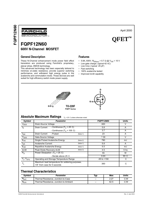
Drain Current Drain Current
- Continuous (TC = 25°C) - Continuous (TC = 100°C) - Pulsed
Gate-Source Voltage
Single Pulsed Avalanche Energy
Avalanche Current
©2000 Fairchild Semiconductor International
Rev. A, April 2000
元器件交易网
FQPF12N60
ID , Drain Current [A]
Typical Characteristics
DS(on) R [Ω], Drain-Source On-Resistance
Repetitive Avalanche Energy
Peak Diode Recovery dv/dt
(Note 1)
(Note 2) (Note 1) (Note 1) (Note 3)
PD
TJ, TSTG TL
Power Dissipation (TC = 25°C) - Derate above 25°C
Parameter Thermal Resistance, Junction-to-Case Thermal Resistance, Junction-to-Ambient
FQPF12N60 600 5.8 3.7 23 ±30 790 5.8 5.5 4.5 55 0.44
-55 to +150
Turn-On Delay Time Turn-On Rise Time Turn-Off Delay Time Turn-Off Fall Time Total Gate Charge Gate-Source Charge Gate-Drain Charge
- 1、下载文档前请自行甄别文档内容的完整性,平台不提供额外的编辑、内容补充、找答案等附加服务。
- 2、"仅部分预览"的文档,不可在线预览部分如存在完整性等问题,可反馈申请退款(可完整预览的文档不适用该条件!)。
- 3、如文档侵犯您的权益,请联系客服反馈,我们会尽快为您处理(人工客服工作时间:9:00-18:30)。
Drain Current - Continuous (TC = 25°C)
- Continuous (TC = 100°C)
IDM
Drain Current - Pulsed
(Note 1)
VGSS
Gate-Source Voltage
EAS
Single Pulsed Avalanche Energy
10.0 V
8.0 V
7.0 V
101
6.0 V 5.5 V
5.0 V
Bottom : 4.5 V
100 10-1
10-1
※ Notes : 1. 250μ s Pulse Test 2. TC = 25℃
100
101
VDS, Drain-Source Voltage [V]
Figure 1. On-Region Characteristics
Units °C/W °C/W °C/W
©2003 Fairchild Semiconductor Corporation
Rev. A, April 2003
FQP13N50C/FQPF13N50C
元器件交易网
Electrical Characteristics
Symbol
©2003 Fairchild Semiconductor Corporation
Rev. A, April 2003
元器件交易网
FQP13N50C/FQPF13N50C
Typical Characteristics
ID, Drain Current [A]
VGS Top : 15.0 V
100
101
V , Drain-Source Voltage [V] DS
Figure 5. Capacitance Characteristics
©2003 Fairchild Semiconductor Corporation
VGS, Gate-Source Voltage [V]
IDR, Reverse Drain Current [A]
DS(ON) R [Ω ], Drain-Source On-Resistance
1.5 VGS = 10V
1.0
VGS = 20V
0.5 ※ Note : TJ = 25℃
0
5
10
15
20
25
30
35
I , Drain Current [A]
D
Figure 3. On-Resistance Variation vs Drain Current and Gate Voltage
ID, Drain Current [A]
101 150oC
25oC 100
-55oC
10-1 2
※ Notes :
1. 2.
V25DS0μ=
40V s Pulse
Test
4
6
8
10
VGS, Gate-Source Voltage [V]
Figure 2. Transfer Characteristics
IS
Maximum Continuous Drain-Source Diode Forward Current
--
--
13
A
ISM
Maximum Pulsed Drain-Source Diode Forward Current
--
--
52
A
VSD
Drain-Source Diode Forward Voltage VGS = 0 V, IS = 13 A
--
--
IGSSF IGSSR
Gate-Body Leakage Current, Forward VGS = 30 V, VDS = 0 V Gate-Body Leakage Current, Reverse VGS = -30 V, VDS = 0 V
--
--
--
--
--
--
1 10 100 -100
td(off)
Turn-Off Delay Time
tf
Turn-Off Fall Time
Qg
Total Gate Charge
Qgs
Gate-Source Charge
Qgd
Gate-Drain Charge
VDD = 250 V, ID = 13 A, RG = 25 Ω
-- 25
60
ns
-- 100 210
2. L =6.0 mH, IAS = 13A, VDD = 50V, RG = 25 Ω, Starting TJ = 25°C 3. ISD ≤ 13A, di/dt ≤ 200A/µs, VDD ≤ BVDSS, Starting TJ = 25°C 4. Pulse Test : Pulse width ≤ 300µs, Duty cycle ≤ 2% 5. Essentially independent of operating temperature
Capacitance [pF]
3000 2500 2000 1500 1000 500
0 10-1
Ciss Coss
Crss
Ciss = Cgs + Cgd (Cds = shorted) Coss = Cds + Cgd Crss = Cgd
※ Notes ; 1. VGS = 0 V 2. f = 1 MHz
TJ, TSTG
Operating and Storage Temperature Range
TL
Maximum lead temperature for soldering purposes, 1/8" from case for 5 seconds
* Drain current limited by maximum junction temperature
FQP13N50C FQPF13N50C
500
13
13 *
8
8*
52
52 *
± 30
860
13
19.5
4.5
195
48
1.56
0.39
-55 to +150
300
Units V A A A V mJ A mJ
V/ns W
W/°C °C
°C
Thermal Characteristics
Symbol RθJC RθJS RθJA
(Note 2)
IAR
Avalanche Current
(Note 1)
EAR
Repetitive Avalanche Energy
(Note 1)
dv/dt
Peak Diode Recovery dv/dt
(Note 3)
PD
Power Dissipation (TC = 25°C)
- Derate above 25°C
Reverse Transfer Capacitance
VDS = 25 V, VGS = 0 V, f = 1.0 MHz
-- 1580 2055 pF
-- 180 235
pF
-- 20
25
pF
Switching Characteristics
td(on)
Turn-On Delay Time
tr
Turn-On Rise Time
D
!
GDS
TO-220
FQP Series
GD S
TO-220F
FQPF Series
G!
●
◀▲
● ●
!
S
Absolute Maximum Ratings TC = 25°C unless otherwise noted
Symbol
Parameter
VDSS
Drain-Source Voltage
ID
Features
• 13A, 500V, RDS(on) = 0.48Ω @VGS = 10 V • Low gate charge ( typical 43 nC) • Low Crss ( typical 20pF) • Fast switching • 100% avalanche tested • Improved dv/dt capability
--
--
1.4
V
trr
Reverse Recovery Time
VGS = 0 V, IS = 13 A,
-- 410
--
ns
Qrr
Reverse Recovery Charge
dIF / dt = 100 A/µs
(Note 4) --
4.5
--
µC
Notes:
1. Repetitive Rating : Pulse width limited by maximum junction temperature
Parameter
TC = 25°C unless otherwise noted
Test Conditions
Min Typ Max Units
Off Characteristics
BVDSS ∆BVDSS / ∆TJ
Drain-Source Breakdown Voltage
Breakdown Voltage Temperature Coefficient
ns
-- 130 270
ns
(Note 4, 5)
--