MA-FL-09-1-orientation
Invitrogen

Quantitation of proliferating cells with the EVOS FL Auto Imaging SystemIntroductionThe Invitrogen™ EVOS™ FL Auto Imaging Systemis a fully automated, digital, inverted multi-channelfluorescence and transmitted-light imaging systemwith outstanding workflow efficiency. Designed tomeet demanding requirements over a broad range ofapplications, it supports high-resolution mosaic tiling,multiple-position well scanning, cell counting withthresholding, and time-lapse studies.Among the versatile software features is cell counting that can be done automatically with a captured or live image. A powerful watershed algorithm has enhanced the precision of counting cells stainedwith Invitrogen™ Molecular Probes™ NucBlue™ Fixed Cell ReadyProbes™ Reagent. Other nuclear stains/fluorescent proteins, or general cytoplasmic fluorescent dyes/proteins, permit the easy determination of total cell numbers and/or percentage of cells stained for a functional readout.In this application note, the number of replicating cells was identified as a percentage of the total population of cells. The percentage of proliferating cells was easily determined by labeling cells with EdU-Alexa Fluor™ 594 to identify proliferating cells and NucBlue Fixed Cell ReadyProbes Reagent to identify total cells. Materials• I nvitrogen™ Molecular Probes™ Image-iT™ Fixation/Permeabilization Kit (Cat. No. R37602)• Invitrogen™ Molecular Probes™ Click-iT™ EdU Alexa Fluor™ 594 Imaging Kit (Cat. No. C10339)• NucBlue Fixed Cell ReadyProbes Reagent (Cat. No. R37606)• Invitrogen™ EVOS™ Light Cube, DAPI (Cat. No. AMEP4650)• Invitrogen™ EVOS™ Light Cube, Texas Red™ (Cat. No. AMEP4655)APPLICATION NOTE EVOS FL Auto Imaging SystemFigure 1. Overlay of 10x image used in the quantitative analysis of proliferating HeLa cells.Figure 2. Screen capture of the quantitation of the totalpopulation of cells (blue) within the image. 373 total cells werecounted in this field of view.Figure 3. Screen capture of the quantitation of the total population of proliferating cells (red) within the image. 138 proliferating cells were counted in this field of view.MethodsHeLa cells grown in a 96-well plate were pulsed with EdU for 1 hour. Cells were fixed, permeabilized and blocked using the Image-iT Fixation/Permeabilization Kit. Following fixation and permeabilization, nuclei were labeled with 2 drops/mL of NucBlue Fixed Cell ReadyProbes Reagent and the incorporated EdU was detected with Alexa Fluor 594 azide (Component B from Cat. No. C10339). Cells with incorporated EdU are shown in pink while all cells have nuclei labeled in blue (Figure 1). Following sample preparation, cells were imaged on the the EVOS FL Auto Imaging System using the EVOS DAPI light cube to visualize NucBlue Fixed Cell ReadyProbes Reagent and the EVOS Texas Red light cube to visualize Click-iT EdU using a 10x objective. Cells were quantitated using the Cell Counting tab on the EVOS FL Auto Imaging System.Results and discussionTotal cell population was determined to be 373 by counting the number of cells in the DAPI channel corresponding to NucBlue Fixed staining (Figure 2). Within this population, the number of proliferating cells was determined to be 138 by counting the number of cells in the Texas Red channel corresponding to Click-iT EdU-positive cells. Based on these results, 37% (138/373) of the cells within this population were shown to be actively proliferating (Figure 3). Using the EVOS FL Auto Imaging System allows researchers to combine qualitative images with quantitative measurements to provide rich data for research applications.Find out more at /evosflautoFor Research Use Only. Not for use in diagnostic procedures. © 2015 Thermo Fisher Scientific Inc. All rights reserved. All trademarks are the property of Thermo Fisher Scientific and its subsidiaries unless otherwise specified. CO017255 0815。
ADS7881EVM, ADS7891EVM Evaluation Module User's Gu

User’s GuideADS7881EVM, ADS7891EVM Evaluation ModuleLijoy Philipose Data Acquisition ProductsABSTRACTThis user's guide describes the characteristics, operation, and use of the ADS78x1 (ADS7881 and ADS7891) 12-bit and 14-bit, parallel, analog-to-digital converter (ADC) evaluation module (EVM). Throughout this document, the terms evaluation board, evaluation module, and EVM are synonymous with the ADS78x1EVM.A complete circuit description, schematic diagram, layout, and bill of materials (BOM) are included in this document.Table of Contents1 Introduction (2)1.1 Features (2)1.2 Analog Interface (2)1.3 Digital Interface (4)1.4 Power Supplies (6)2 Using the EVM (7)3 ADS78x1EVM Bill of Materials (8)4 ADS78x1EVM Layout (10)5 ADS78x1EVM Schematics (14)6 Revision History (17)List of FiguresFigure 1-1. ADS7881 Input Buffer Circuit (3)Figure 2-1. Decoding Control Signals Using the Address Bus (7)Figure 4-1. Top Layer – Layer 1 (10)Figure 4-2. Ground Plane – Layer 2 (11)Figure 4-3. Power Plane – Layer 3 (12)Figure 4-4. Bottom Layer – Layer 4 (13)Figure 5-1. Schematic Page 1: Digital Buffer (14)Figure 5-2. Schematic Page 2: ADS7881, ADS7891 (15)Figure 5-3. Schematic Page 3: Digital Communication (16)List of TablesTable 1-1. Related Documentation from Texas Instruments (2)Table 1-2. Analog Input Connector (2)Table 1-3. Solder Short Jumper Setting (4)Table 1-4. Pin Out for Parallel Control Connector P2 (4)Table 1-5. Jumper Settings (5)Table 1-6. Data Bus Connector P3 (5)Table 1-7. Pin Out for Converter Control Connector J3 (6)Table 1-8. Power-Supply Test Points (6)Table 1-9. Power Connector, J1, Pin Out (6)Table 3-1. Bill of Materials (8)TrademarksAll trademarks are the property of their respective owners.Introduction 1 IntroductionThe ADS78x1EVM showcases the 12-bit, 4-MSPS (ADS7881) and 14-bit, 3-MSPS (ADS7891) ADCs. TheADS7881 and ADS7891 devices include a capacitor-based successive-approximation register (SAR) ADC with inherent sample and hold. These devices offer either a 12-bit or 14-bit parallel interface. Both devices offer byte mode operation that enables easy interface with 8-bit processors. They also have a pseudo-differential input stage and a 2.5-V internal reference.This evaluation module serves as a reference design and a low-cost method to test these converters in the end application. The following sections describe the pin outs of the various analog, power, and digital connectors and power requirements.Table 1-1 lists documents related to the ADS78x1EVM.1.1 FeaturesThe ADS78x1EVM includes the following features:•Full-featured evaluation board for the high-speed, SAR-type ADS7881(12-bit, 4-MSPS) or ADS7891(14-bit, 3-MSPS) single-channel, parallel interface ADCs•Onboard signal conditioning•Onboard reference•Input and output digital buffers•Onboard decoding for stacking multiple EVMs1.2 Analog InterfaceThe ADS7881 and ADS7891 ADCs have both a positive and negative analog input pin. The negative input pin, which has a range of –200 mV up to 200 mV is shorted on the board. A signal for the positive input pin can be applied at connector P1, pin 2 (as shown in Table 1-2) or at the center pin of the SMA connector J2.(1)All odd-numbered pins of P1 are tied to AGND.1.2.1 Signal ConditioningThe factory recommends the analog input to any SAR-type converter be buffered and low-pass filtered. The input buffer on the ADS78x1EVM uses the THS4031 (as shown in Figure 1-1) configured as an inverting gain of one. However, the amplifier is not stable at a gain of one, and is thus configured for inverting gain of one. The THS4031 was selected for its low noise, high slew rate, and fast settling time. The low-pass filter resistor and capacitor values were selected such that the ADS78x1EVM meets the 1-MHz AC performancespecifications listed in the data sheet. The series resistor works in conjunction with the capacitor to filter the input signal, but also isolates the amplifier from the capacitive load. The capacitor to ground at the input of the ADC works in conjunction with the series resistor to filter the input signal, and functions as a charge reservoir. This external filter capacitor works with the amplifier to charge the internal sampling capacitor during sampling mode. Resistors R1 and R12 were selected to reduce offset.The EVM has a provision to offset the input voltage by adjusting R25, a 10-kΩ potentiometer.130 pF(+)IN(−)INCCV IN10 k Figure 1-1. ADS7881 Input Buffer Circuit IntroductionIntroduction 1.2.2 ReferenceThe ADS78x1EVM provides an onboard 2.5-V reference circuit. The EVM also supplies a reference voltage via connecter P1 pin 20. This reference voltage can be filtered through amplifier U1. The converter itself has on-chip reference buffer, and therefore does not need to be buffered externally. The reference buffer circuit on the EVM is used to generate the offset voltage for the input amplifier, U2.The EVM allows selection from three reference sources. Set SJP1, SJP2, and SJP4 to select either an onboard reference voltage (REF1004-2.5), ADC internal reference, or a user-supplied reference voltage via P1 pin 20. Table 1-3 lists jumper settings and Section 5 provides full schematics.(1)Factory-set condition.1.3 Digital InterfaceThe ADS78x1EVM is designed for easy interfacing to multiple platforms. Samtec part numbers SSW-110-22-F-D-VS-K, TSM-110-01-T-DV-P, SSW-116-22-S-D-VS, and TSM-116-01-T-D-V-P provide a convenient dual row header and socket combination at P1, P2, P3, and J3. Consult Samtec at or 1-800-SAMTEC-9 for a variety of mating connector options.Connectors P1, P2, and P3 allows the user to plug the EVM into the 5-6k interface card to interface directly with the TMS320C5000 and TMS320C6000 series of DSP. Table 1-4 lists the connector pin out.(1)All even-numbered pins of P2 are tied to DGND.Read (RD), conversion start (CONVST) and reset (RESET) signals to the converter can be assigned to two different addresses in memory via jumper settings. The jumper settings allow up to two ADS78x1EVMs to be stacked into processor memory. See Table 1-5 for jumper settings. The evaluation module does not allow the Introduction chip-select (CS) line of the converter to be assigned to different memory locations. Instead, ground or wire the CS line to an appropriate signal of the user processor.(1)Factory-set condition.The data bus is available at connector P3. Table 1-6 lists the pin out information. This EVM supports two devices but the connector signals names are based on the ADS7981, which is the higher-resolution device. Depending on which device is being evaluated, care must be taken when connecting the EVM to a host processor.(1)All even-numbered pins of P3 are tied to DGND.As described in Table 1-7, this evaluation module provides direct access all the analog-to-digital converter control signals via connector J3.(1)All even-numbered pins of J3 are tied to DGND.1.4 Power SuppliesThe EVM accepts four power supplies.• A dual ±Vs DC supply for the dual-supply op amps. A ±12-V DC supply is recommended.• A single +5.0-V DC supply for the analog section of the board (ADC + reference).•A single +5.0-V or +3.3-V DC supply for the digital section of the board (ADC + address decoder + buffers).There are two ways to provide these voltages.1.Wire in voltages, as listed in Table 1-8, at test points on the EVM.e the power connector J1 and derive the voltages elsewhere.Table 1-9 lists the pin out connections forJ1. Set jumper W5 to short between pins 1-2 or pins 2-3 to short +3.3VD or +5VD, respectively, to be the buffer digital supply (+BVDD).Introduction Using the EVM2 Using the EVMThe ADS78x1EVM serves as a reference design, prototype board, and test platform for the software engineer to develop code.As a reference design, the ADS78x1EVM contains the essential circuitry to showcase the ADC. This essential circuitry includes the input amplifier, reference circuit, and buffers. The EVM analog input circuit is optimized for a 1-MHz sine wave, therefore users may need to adjust the resistor and capacitor values of the ADC input RC circuit. In AC-type applications where signal distortion is a concern, use polypropylene capacitors in the signal path. In applications where the input is multiplexed, either adjust or remove the ADC input resistor and capacitor, as needed.As a prototype board, the buffer circuit consists of a footprint in a standard 8-pin SOIC and resistor padsfor inverting and noninverting configurations. The ADS78x1EVM can be used to evaluate both dual- and single-supply amplifiers. The EVM comes installed with a dual-supply amplifier that allows the user to take advantage of the full input voltage range of the converter. For applications that require signal supply operation and smaller input voltage ranges, the THS4031 can be replaced with a single-supply amplifier, such as the OPA300. Short pad jumper SJP7 between pads 1 and 2, because SJP7 shorts the minus supply pin of the amplifier to ground. The positive supply voltage can be applied via test point TP12 or connector J1 pin 1.As a software test platform, connectors P1, P2, and P3 plug into the parallel interface connectors of the 5-6K interface card. The 5-6K interface card sits on the C5000 and C6000 digital signal processor starter kit (DSK). The ADS78x1EVM is then mapped into the processor memory space. This card also provides an area for signal conditioning. This area can be used to install application circuits for digitization by the ADS7881 or ADS7891 ADC. See the 5–6K Interface Board user's guide for more information.For the software engineer, the ADS78x1EVM provides a simple platform for interfacing to the converter. The EVM provides standard 0.1" headers and sockets to wire into prototype boards. The user must only provide three address lines (A2, A1, and A0) and one address valid line (DC_CS) to connector P2, as shown in Figure2-1. To choose which address combinations generate RD, CONVST, and RESET set jumpers as shown in Table 1-5. Recall that the chip select (CS) signal is not memory mapped or tied to P2, and therefore must be controlled via a general-purpose pin or shorted to ground at the J3 pin 1. If address decoding is not required, the EVM provides direct access to converter data bus via P3 and control via J3.A1A2DC_CSFigure 2-1. Decoding Control Signals Using the Address Bus4 ADS78x1EVM LayoutFigure 4-1 to Figure 4-4illustrate the silkscreens for the ADS78x1EVM.Figure 4-1. Top Layer – Layer 1ADS78x1EVM Layout Figure 4-2. Ground Plane – Layer 2 ADS78x1EVM LayoutFigure 4-3. Power Plane – Layer 3ADS78x1EVM Layout Figure 4-4. Bottom Layer – Layer 4 ADS78x1EVM Layout Revision History6 Revision HistoryChanges from Revision * (December 2004) to Revision A (October 2021)Page •Changed document title from ADS7881/ADS7891EVM to ADS7881EVM, ADS7891EVM Evaluation Module1•Changed ADS7881/ADS7891EVM to ADS78x1EVM throughout document (1)•Added Related Documentation from Texas Instruments table to Introduction section (2)•Changed paragraph preceding Data Bus Connector P3 (4)•Changed Data Bus Connector P3 table (4)IMPORTANT NOTICE AND DISCLAIMERTI PROVIDES TECHNICAL AND RELIABILITY DATA (INCLUDING DATA SHEETS), DESIGN RESOURCES (INCLUDING REFERENCE DESIGNS), APPLICATION OR OTHER DESIGN ADVICE, WEB TOOLS, SAFETY INFORMATION, AND OTHER RESOURCES “AS IS” AND WITH ALL FAULTS, AND DISCLAIMS ALL WARRANTIES, EXPRESS AND IMPLIED, INCLUDING WITHOUT LIMITATION ANY IMPLIED WARRANTIES OF MERCHANTABILITY, FITNESS FOR A PARTICULAR PURPOSE OR NON-INFRINGEMENT OF THIRD PARTY INTELLECTUAL PROPERTY RIGHTS.These resources are intended for skilled developers designing with TI products. You are solely responsible for (1) selecting the appropriate TI products for your application, (2) designing, validating and testing your application, and (3) ensuring your application meets applicable standards, and any other safety, security, regulatory or other requirements.These resources are subject to change without notice. TI grants you permission to use these resources only for development of an application that uses the TI products described in the resource. Other reproduction and display of these resources is prohibited. No license is granted to any other TI intellectual property right or to any third party intellectual property right. TI disclaims responsibility for, and you will fully indemnify TI and its representatives against, any claims, damages, costs, losses, and liabilities arising out of your use of these resources.TI’s products are provided subject to TI’s Terms of Sale or other applicable terms available either on or provided in conjunction with such TI products. TI’s provision of these resources does not expand or otherwise alter TI’s applicable warranties or warranty disclaimers for TI products.TI objects to and rejects any additional or different terms you may have proposed.Mailing Address: Texas Instruments, Post Office Box 655303, Dallas, Texas 75265Copyright © 2022, Texas Instruments Incorporated。
Alma以色列飞顿激光光子工作站
第7页,共43页。
患有肿瘤,特别是皮肤癌
妊娠
使用光敏感的药物 患有对光敏感的疾病的
最近3-4周在阳光下暴晒或是日光浴的或是即将接 受阳光暴晒的
活跃性的单纯性疱疹 糖尿病
内分泌失调
疤痕体质 干性敏感皮肤
第8页,共43页。
癫痫症
使用抗凝药物 曾患有血液凝固性病变
1、治疗区域需涂消炎药膏(如红霉素软膏、金霉素软膏或 百多邦等)2天,每天2次,以防感染,注意涂抹的次数
不能过多,否则会影响痂皮的形成。
2、恢复期间治疗区域勿碰水,勿进行皮肤护理、勿化妆及
勿搓擦。
3、恢复期间不宜进行剧烈运动,以免太多的出汗导致皮肤
感染或延缓修复过程。
第41页,共43页。
三、激光、光子
观察终点:痤疮颜色变暗或痤疮变蔫
脉宽选择:Ⅲ--Ⅳ皮肤选择40ms脉宽
第19页,共43页。
由于AFT420nm波长短、穿透较浅,治疗时能量尽量控制在 12J或以下,以免引起水疱。在12J治疗效果不理想的情况下 可适当增加到13J,14—15J的能量慎用。
第20页,共43页。
第21页,共43页。
第22页,共43页。
第9页,共43页。
在患者第一次就诊时,医生应该告知患者以下内容
➢激光光子的治疗是一项综合治疗,一般需要多次治疗; ➢治疗时可能会有一些不适的感觉,有些人感觉是轻微疼痛; ➢治疗结束后可能出现一过性的红斑/水肿; ➢皮肤整体的改善需要几个月的时间逐渐的完成;
➢可能会出现的副作用如色素改变等,通常为一过性的。
570-950nm
治 疗: 雀斑、老年斑、提亮肤色等 能量选择:12--18J/cm2 疗 程:3--4周一次, 4--6次为一个疗程 观察终点:皮肤微红(色斑颜色加深) 脉宽选择:Ⅲ--Ⅳ皮肤选择12ms脉宽
OLED Displays Design Guide for Active Matrix OLED(AMOLED) Displays

Introduction to OLED Displays Design Guide for Active Matrix OLED (AMOLED) Displayslast updated 22 May 2008Introduction•Active Matrix OLED (AMOLED) is a new display technology that is rapidly becoming viable for many applications.•It has some undoubted benefits over competing technologies.•4D holds no responsibility or liability for the accurateness of the information and how it is applied to any design.What is an OLED?•OLED (Organic Light-Emitting Diode) is a self light-emitting technology composed of a thin, multi-layered organic film placed between an anode and cathode. In contrast to LCD/TFT technology, OLED does notrequire a backlight.How does an OLED emit light?•OLED’s basic structure consists of organic materialspositioned between the cathode and the anode, which is composed of electric conductive transparent Indium Tin Oxide (ITO). The organic materials compose amulti-layered thin film, which includes the HoleTransporting Layer (HTL), Emission Layer (EML) andthe Electron Transporting Layer (ETL). By applying the appropriate electric voltage, holes and electrons areinjected into the EML from the anode and the cathode, respectively. The holes and electrons combine inside the EML to form excitons, after whichelectroluminescence occurs. The transfer material,emission layer material and choice of electrode are the key factors that determine the quality of OLEDcomponents.Comparison between OLED and TFT DisplayFigure 1 -AMOLED Figure 2 –TFT Display AMOLED has less complexity so is much thinnerActive vs Passive Matrix•4D Systems offers both the Active Matrix and the Passive Matrix OLED modules.•Passive Matrix is low cost but can only be manufactured economically in colour to a size of 1.69”(160x128pixels). Standard industry sizes for colour PMOLED is 0.95”(96x64) and 1.5”(128x128). Most of the new development is in Monochrome Displays using White, Blue or Yellow colouring.So what’s the difference?•AMOLED, the array is divided into a series of row and column lines, with each pixel formed at the intersection of a row and column line, just as in a passive-matrix display. Each pixel now consists of an OLED in series with a thin-film transistor (TFT). The TFT is a switch that can control the amount of current flowing through the OLED. In AMOLED, information is sent to the transistor in each pixel, dictating the brightness of the pixel. The TFT then stores this information and continuously controls the current flowing through the OLED. In this manner the OLED is operating continuously, avoiding the need for the very high currents necessary in a passive-matrix display.•In PMOLED to illuminate any particular pixel line a passive-matrix display, electrical signals are applied to the row line and column line. The more current pumped through each pixel diode, the brighter the pixel.Advantages of AMOLEDThe major competing technology for AMOLED is TFT displays. AMOLED is higher priced (anywhere from 50-100% depending on the comparable screen size), so why would you choose AMOLED? Here are 8 compelling reasons:1.High C/R2.Wide Temperature Operation3.Fast Response4.High and Constant colour Gamut5.Wide Viewing Angle6.Peak Brightness7.Low Power Consumption8.Very Slim designEach of these advantage will be discussed in more detailHowever AMOLED does have some technology issues which means it is not suitable for all applications.1.Price2.Image Sticking/Image Retention3.LifetimeA description of the issues and design guidelines about how to overcome these are also discussed.Remember: 4D also offers many TFT solutions and we are not degrading the technology in anyway. It is important that you choose the best technology for your application andyour budget.High Contrast RatioOLED TFTConclusion–higher contrast ratio gives impression for higher brightness. OLED is much better than Transmissive TFT for Sunlight readabilityConstant Contrast Ratio –wide viewing angleHigh Ambient Contrast RatioCONCLUSIONOLED Looksbetter in allconditionsFAST Response TimeOLED LCD TFT<50uS3000~30000uS Fast response time means full motion graphics can bedisplayedFAST Response TimeWide Temperature OperationOLED can work from-40 ~85C TFT can work from -20 ~70COther technologies (e.g. CSTN, Mono LCD) have significant problems at temperature extremesHigh Temperature –Liquid Crystal is disturbed and can’t be controlled by an electric fieldLow Temperature -Liquid crystal is unresponsive and becomes slowSignificantly higher Colour GamutGamut%Gamut%Lv%Lv%OLEDLCDTFT Constant Colour Gamut at all gray levelsOLED looks brighter, sharper and more visually pleasingWide Viewing Angle with Smaller Degradation of Optical PerformanceVisually Perceived Brightness•Even at the same luminance, High C/G image looks brighter. •High C/R image looks brighter.Brightness based on 200nit 2.4”AMOLED Display•TFT display has constant current as backlight which must be on no matter what picture is displayed.•Conclusion –use Black background on OLED to minimise powerAverage Power ConsumptionAMOLED power consumption depends on image content & application.•Black background can save more power.•Moving image is a good application.How to Lower Power Consumption AMOLED power consumption can bedecreased by:• 1. Black background. ( 50%~80% ) ↓• 2. Lower full white brightness. Ex.200nits 160 nits. ( 20% ) ↓• 3. Auto current limit driving method.(20% ) ↓• 4. OLED material & device efficiencyincrease. (30% ) ↓Slim Thickness •Future improvementsIMAGE STICKING•Image sticking is the terms used to describe the image retention occuring when a fixed pattern is displayed over a prolonged period of time.•For example, if we continuously displayed the checker board pattern like the picture shown on the bottom left for a long time, and switch to 50%Gray of full whitepattern, we can see the image like the right one, the phenomenon we call is Image Sticking. (Full White is 200nits, 50% is 100nits)For techniques to overcome image sticking see slides in the design guideDESIGN USER GUIDE FOR AMOLED DISPLAYS•With some of the advantages and features of AMOLED it is important to consider these in your design to maximise the benefits of the technology.•The following pages give design guidelines, recommendations and tips. Methods to overcome some of the technical limitation are also given for your reference.Design GuideIn any good Graphic User Interface (GUI) design you need to consider : power saving, image retention & image sticking.Therefore it is recommended the GUI has a Black Background, with white or coloured text & icons because of:Lowest power consumptionNo image sticking problemIn case of white or colour words & icons, R,G,B gray scale should be less than 80% of full gray scale. Because of the high contrast ratio between background and foreground, the perceived brightness is brighter than it really is. Meanwhile power consumption is further lower and it isgood to reduce any image sticking.IMAGE Sticking -TestingTest using 2.8”AMOLED was made and decay ratio after 24 hours was measuredConclusion –if displaying static images e.g. for industrial data-logger application –use Green to minimise image sticking. Avoid BlueImage StickingLow brightness is good; especially for small icons & text.Because of OLED peak brightness & higher contrast, when we show text or small icon on black background, the icon brightness can be decreased by lower gray scale.Low colour Temperature < 6500K design for small icon & text.Image sticking comes more from Blue since its OLED life time is shorter than Red and Green. Using lower colour temperature for text or small icons on black background is good for preventing the Image from sticking.Always use white or coloured text with black background during operation.→→√XGoodDesignBadDesignAvoid using the same icons on different GUI. This will ensure that image sticking is minimised.Power Consumption MinimisationTo minimise power consumption, select black, colourful or graphic backgrounds . Do not use a white background.Design Guidelines•Do not use black words with white selection bar since white has the highest power consumption.•White words with colour selection bar is a better design to minimise image sticking.Lifetime•Panel lifetime specification is currently 20K hours (time to half intensity)•However each colour RGB has a different lifetime.–Green is the best at 40K hours, Red is 25K and Blue is 12K hours.•With this in mind it is important to consider your colour choices on your GUI. Where possible avoid blue.•When you consider image sticking and lifetime of each of the colours you can quickly see most of the technology limitations are reduced significantly if you avoid blue! For example in an industrial application where you might have data displayed for long periods,display in green to avoid image sticking.Summary of Design Guidelines•GUI with black, graphic or colourful background is necessary for AMOLED display.•For white text & icon, it is not necessary to use full gray scale (N= 64 or 255). 80% (N<50 or <200) is enough.•Try to design colourful text or icons, where the colour temperature is lower than 6500K. On the other hand, decrease the blue gray scale as much as possible. (NB<30 or <125)•Always use white or coloured text in black background during operation.•When GUI is changing, the black to black background change is recommended to minimise image retention.•Try not to let the icon remain fixed at the same location.•The panel should be turned off automatically whenever possible to increase lifetime and eliminate image sticking.。
CDMA射频测试作业指导书

检验指导书
指导书名称 CDMA 射频测试作业指导书
编号
1900M 频段的最大输出功率为 18dBm~27dBm (当有与国标规定不一致时,具体参考公司现行各产品的技术更改通知单) 最小受控输出功率: 最小输出功率将小于 –50dBm/1.23MHz
页次 第 9 页 共 12 页
3)接收机的灵敏度 按“硬 F7”键将“Cell Power”设置为-65.00dBm; 呼通后将信道改成希望测试的信道;如 450M(A 段):160、210、260;450M(C 段):47、97、 147;800M:384、777、1013;1.9G:100、525、1125 等等; 按右“more” →“2 of 3”按“硬 F7”键设置成“Alternating bits”; 按“CALL SETUP”返回主界面; 按“硬 F11”键对 Radio config 进行设置,如果是进行 RC1 的灵敏度的测试,此时设置为 (Fwd1,Rvs1)/S02(loopback);如果是进行 RC3 的灵敏度的测试,此时设置为(Fwd3,Rvs3) /S055(loopback); 按“硬 Measurement selection” →“Frame Error Rate” →“硬 F1” 将“FER requirement”设置 0.5%;
按“硬 F11”键对 Radio config 进行设置,如果是进行 RC1 的波形质量和频率误差的测试,此时 设置为(Fwd1,Rvs1)/S02(loopback);
按“硬 Measurement selection” 选择“Waveform Quality”;按“硬 F1”/“Waveform Quality Setup” 将“Multi-Measurement Count”点亮并输入“10”次;
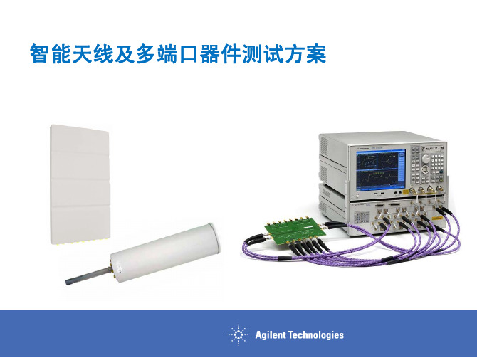
智能天线及多端口器件测试方案
优点 成本最低 按用户需求定制 单次连接 全多端口校准
缺点 需要多次连接,效率低 开关切换速度有限 成本高
NAFO 09
Agilent Confidential
2009/12/28
4端口网络仪+开关矩阵+定制软件
成功案例:中国移动研究院、西安海天、南京 捷士通、武汉虹信 配置: ENA+Z5623AH08+82357B+VBA SW+N4431B+test cables
Agilent智能天线测试系统主界面
显示区域1:通道1~9:天线8个端口和校准端口反射参数测试
显示区域2:通道11,12: 传输幅度相位参数相对比值结果
智能天线多通道测试 结果显示窗口
显示区域3:通道13~20:天线每个端口到校准端口传输参数
显示区域4:通道21~27:天线每个端口隔离参数测试
测试控制窗口
NAFO 09
Agilent Confidential
2009/12/28
测试报告
NAFO 09
Agilent Confidential
2009/12/28
Agenda
1 智能天线及多端口器件测试概述 2 智能天线天线测试方案
3 多端口器件测试方案
NAFO 09
Agilent Confidential
U3042AE12 (16-port)
Z5623AK66 (14-port)
E5091A-009 (9-port)
Z5623AK44 (8-port) Option 5ቤተ መጻሕፍቲ ባይዱ0 with N44xxB (4-port) Z5623AK64 (6-port) High Power
英语6000词汇(打印版).

赵丽词汇课堂介绍1一、计划本课程词汇集中在2000~6000,都是一些基本的词汇,生活中常用的词汇,背单词要有目的性,清楚自己参加什么考试,要有针对性,才更有热情。
根据自己是哪类人,在一星期内复习相关词汇,力求反复掌握。
背单词过程:看-认-背-用。
现阶段只停留在前两阶段。
背单词一次只需了解1~2个词意,然后在阅读中不断扩展。
可用新概念4做为阅读材料,定期背诵。
二、英语单词的构成1、基础词汇:无特别记忆、需建立与汉语词意间的联系naive 天真的——奶壶,喝奶的孩子很天真2、希腊神话(听故事记单词)tantalus(本能的)诱惑v.——人名,宙斯与人类之子,出自希腊神话tantalize 逗引或招惹rim 边缘——只有rim是边缘brim 边缘——前面加b含义不变grim 恐怖的——前面加g(鬼)真恐怖trim 修剪整齐——前面加t才修剪整齐prim 呆板的——p在rim前真呆板prose 单调、散文——扑(p)到玫瑰上更单调plight 困境——扑(p)灭了光就陷入困境pray 祈祷——扑(p)在光线下才是祈祷课堂介绍 23、外来词汇chaos 混乱、紊乱——吵死flirt 调情——抚摸着她,逗她笑quaint 古怪的——拼音guai,怪acquaint 熟悉,见怪不怪——ac前缀,一再。
charisma 领袖气质——中国(ch)升起了(aris)毛泽东(ma)orison 祈祷——太阳(o)升到半空(rison),于是祈祷mirth 高兴的——妈妈(m)看到你出生(irth)很高兴blear 模糊——不(b)清楚(lear)clear 清晰拉丁语系讲究构词法,重点记忆词根、词缀pose 姿势、v.放——词根expose 暴露——前缀ex:出来,放在外面=暴露compose 组成——前缀com:共同,共同放在一起=组成decompose 分解——前缀de:向下,把组成的东西向下=分解depose 免职——前缀de:向下,pose放,向下放=免职despise 轻视、蔑视——前缀de:向下;spit:吐口水;低头吐口水=轻视deposit 存款、下蛋、沉淀物——前缀de=向下;pos:放出来;向下放出来=下蛋repose 休息——前缀re:放回来,往回,反复;放回去->休息reticent 沉默不语的——re:阿姨;ti:提;cent:分,钱;阿姨提钱->沉默不语的intimate 亲密的——在心里总提(ti)到他,特指情侣间的亲密vigorous 精力充沛的——vi:六;go:个;rous:人;一个人具备六个人的精力->精力充沛的[liberty:流鼻涕没人管->自由]三、谐音记忆法ponderous 笨重的——胖的要死->笨重boff 狂笑——暴富->狂喜quaff 痛饮——夸父,追日极渴->痛饮sting 蜇、咬——死叮scowl 皱眉头——思考exhaust 耗尽、精疲力尽的——一个早死的他robust 强壮的——乐百氏,四肢发达,头脑简单luxury 奢侈——力士香皂,住在天河(milkway)边的仙女的皮肤->奢侈Nike 胜利女神——耐克,希腊神话中的胜利女神caste 等级制度——卡死他frugal 节俭的——腐乳就够了->节俭miserly 小气的、吝啬的——小气鬼李先生3、代码联想记忆法loom v.若隐若现n.织布机bloomv.开花blast 爆炸ignite v.点燃ignore v.忽视ostrich n.鸵鸟stigma 耻辱、污点stroll 闲逛stink 恶臭prestige 名声、名誉gloom 郁闷的abide 忍受孤独的absurd 荒谬的echo 回声echolocation 回声定位amorous 好色的morose 郁闷的4、行之有效的记忆法:向别人复述单词3遍第1课第1题1. Living in that _____ house over there hasnearly driven the hero of the story mad.A. bleakB. hauntedC. gauntD. acumenbleak 荒凉的——不(b)漏水(leak)也是荒凉的leak 漏,漏水gaunt 憔悴的,苍白的——鬼(g)阿姨(aunt)的脸色苍白憔悴,考GRE(g)的姑姑(aunt)脸色憔悴vaunt 吹牛——五个(v)姑姑/大娘(aunt)在一起吹牛flair 天赋,本能——天(air)高任鸟(fl)飞flee 逃离,逃跑——飞离(谐音)flaunt 炫耀——飞(fl)姑姑(aunt),小龙女,为了引人注目而炫耀haunt 常来常往的地方,鬼神出没的地方——姑姑(aunt)家(h)是常来常往的地方jaunt 短途旅行——短途旅行回来,去接(j)姑姑(aunt)daunt 恐吓,威胁——打(d)姑姑(aunt)->威胁saunter 闲逛,四处逛acumen 敏锐,聪明——男人(men)削尖了脑袋->明智的男人;阿Q们acute 尖的,敏锐的,灵敏的,急性病cute 可爱的,聪明的chronic 慢性病,慢性的acupuncture 针灸——用尖的东西(acu)来点(puncture)->针炙punctual 准时的,按时的punctuation 标点第1课第2题2. His body temperature is ______ for three days,the highest point reaching to 40.5 degreecentigrade.A. uncommonB. disorderedC. abnormalD. extraordinarycentigrade (摄氏)温度century 世纪,百年——centipede 蜈蚣——百(centi)脚(pede)动物->动物biped 两足动物——bi(两)ped(脚)paddle 踏板,桨——脚蹬、踏板percent百分比——per(每)cent(百)cent 分,一分钱decent 合适的,体面的,正派的——冲着钱(cent)的面子de(低头)->待遇是合适的、体面的indecent 不合适的,下流的,不妥当的——in:否定前缀innocent 无辜的,天真的,单纯的——我的兜里(in)没有(no)一分钱->无辜的;孩子兜里没有一分钱->天真的incentive(金钱方面的)鼓励,刺激reticent 沉默不语的——阿姨提到钱intimate 亲密的——在心里老提到的那个人intimate relationship 亲密的关系grade 年级degrade 降级——de向下upgrade 升级——up上升degraded 低级的,品位低俗的degrade tast 品位低俗的despite 蔑视,鄙视split 分裂,分开——用l把spit分开wallflower 壁花,丑小鸭,局外人abnormal 不正常的,异常的,反常的——离开(ab)标准(normal)->反常normal 标准的adj.norm 标准n.abide 忍受,遵守(法律法规)abuse 滥用(职权)——离开(ab)正常的使用范围(use)->滥用enormous 相当多的,大量的,巨大的——超出(e)标准的->大量的tremendous 巨大的,高速的,可怕的——令人颤抖(trem)的结果(end)->可怕的tremble 颤抖——船泊在水中晃at tremendous speed 以极快的速度irritate 激怒irritable 激怒的——激怒的是桌子(table)irrigate 灌溉——灌溉的是大门(gate)castigate 惩罚,严惩——扔掉(cast)大门(gate)受惩罚tolerance 忍耐力,耐受力tolerate 忍受,容忍disguise 伪装——dis不是,gui->guy家伙,不是那个却半夜成那个->伪装disgust 恶心的,肮脏的,下流的——把自己伪装成她(如花)->恶心repulsive 恶心的——(小强在你的胳膊上)反复蹦pulse 心跳,脉搏retch 干吐,恶心wretch 悲惨,不幸的人——我(w)吐也吐不出来awfully 恶心的,非常,可怕的You are awfully beautiful. 你非常美common 平常的,普通的the common person 老百姓,平民,大众uncommon 不常见的,不普通的——un否定前缀common sense 有常识的nonsense 性情古怪的,胡说八道commonplace 平凡的,平庸的,陈腐的——平常地方所见的都是平凡的order 顺序disorder 杂乱无章,使神经错乱,混乱——dis 否定前缀discover 发现cover 覆盖close 关闭disclose 揭示,揭露like 喜欢dislike 不喜欢,讨厌mentally disordered 精神错乱mantle 地幔crust 地壳core 地核,核心sentimental 感伤的,伤感的,多愁善感的——三屉馒头,吃了N多必须减肥,愁啊delicate 娇弱的,纤细的,(皮肤)细腻的,敏感的,哀婉的,(五官)精致的,精细的(尤指眼科手术),(化装,颜色,味道)淡淡的——林黛玉同学……第2课第1题3. Texas, the second largest state of America, is_______ in natural resources.A. wealthyB. abundantC. scatteredD. depositedabundant 丰富的,充裕的redundant 多余的,过剩的——red(红)undantabsurd 荒谬的,可笑的——爱不死的(谐音),很荒谬ambiguous 模棱两可的,似是而非的——两边(ambi),安必归(治精神病的良药)ambience 环境deposit 下蛋,沉积物,存款——de(向下)pos(下放)expose 暴露repose 休息compose 组成,作曲impose 强加于,征税——往里(im)放(pos)propose 提出建议,求婚——往前(pro)放(pos)depose 免职,降职decompose 分解第2课第2题4. _____ to some parts of South America is stilldifficult, because parts of continent are stillcovered with thick forests.A. OrientationB. AccessC. ProcessionD. Blightorientation 东方,定位oriental 东方的——o(太阳)ri(升起)ent(进入)orison 祈祷ray 光线prim 呆板prose 散文,诗歌,平淡无奇plight 困境pray 祈祷plunge into 投入,跳入(水中)——中间有个肺lung 肺enter 进来potential 潜力,潜能——pot(罐子)ent(进入),联想阿拉丁的灯神permanent 永久的,永恒的——per(每个)man(男士)ent(进入)一种追求永恒爱情的境界eternal 永恒的,永久的Eternal City 永恒的城市,罗马pledge 发誓pledge one's eteranl love 发山盟海誓eternal fire 长明灯internal 内部的external 外部的access 接近——cess词根表示走路have access to 接近,使用process 前进,加工——pro(往前)cess(走)procession 队列,行列recession 休息,(企业)停业整顿——re(阿姨)cess(走,回来),停业excess 过度,过分,剩余——ex(过度)cess(走)concession 妥协,让步——con(共同,各)cess(各走一步),妥协incessant 不断的,连续的blemish 缺点,污点——blie(布来)mish(迷失),是污点blot 肮脏,污点——虽然不(b)多(lot),但也很脏blight 枯萎——b(不)light(光),见不到光就枯萎blast 爆炸——b(不)last(持续),就爆炸blame 责备,责怪——炸坏了腿(lame),别(b)怪我第2课第3题5. I hope my teacher will take me recent illnessinto _____ when judging my examination.A. accountB. countingC. regardD. observationcount 计算account 计算,说明——ac(一再)count(数),考虑take into account 考虑在内count (me) in 算我一个count (me) out 别算我countless 数不过来的,不计其数的regard (as) 认为regard 凝视,注视best regards 最好的祝福XXOO 亲亲抱抱regardless (of) 不管,不顾peep 偷窥glimpse 一瞥love at first glimpse 一见钟情leer 斜视,送秋波gape 吃惊地看——g(看到)ape(猿猴)ape 猿猴nightmare 噩梦——夜(night)里看到床上一个母马(mare),噩梦mare 母马gaze 凝视,(感兴趣地)看illusion 幻觉——(谐音)一路走近的美女是幻觉illuming 照亮,点亮——(谐音)一路明observation 观察,引用,评述reference 典故commentary 评论,解说penalty 点球,惩罚该组:观察储备,觉得是值得保存的:observe 观察,遵守reserve 储备deserve 值得conserve 保存conservation 保存conservative 保守的reservation 印第安人保留地第3课6. I'd ____ his reputation with other farmers andbusiness people in the community and then makea decision about whether or not to approve a loan.A. take into accountB. account forC. make up forD. make outreputation 名誉,声望——re(重复)put(计算)ationcompute 计算computer 计算机prestige 声望,威信——pre(前面)st(街)上……nasty 肮脏的,下流的,恶心的——na(那)st(街)上为(y)何什么那么脏一个故事:……申请(apply)留学,获得批准(approve),非常感激(appreciate)新东方。
NI ELVIS产品介绍说明书

PRODUCT FLYERNI Educational Laboratory Virtual Instrumentation Suite (NI ELVIS)CONTENTSNI ELVISDetailed View of NI ELVIS IIIKey FeaturesNI ELVIS III Soft Front PanelsNI ELVIS III with Multisim Live™NI ELVIS III with MathWorks Simulink®NI ELVIS III Application Programming Interface (API)Hardware ServicesNI ELVISNI ELVIS III, NI ELVIS II+, and NI ELVIS II•Software includes interactive web and desktop soft front panels, instrumentation support for Windows and Mac, API support for LabVIEW and text-based languages, shipping examples,and detailed help files•Seven hardware instruments plus control I/O containing 16 AI, 4 AO, and 40 DIO•4-channel, 100 MS/s (400 MS/s single channel), 50 MHz oscilloscope with 14-bit resolution•16-channel, 100 MS/s logic analyzer/pattern generator•16-channel, 1 MS/s analog input with 16-bit resolution•40 DIO lines individually programmable as input, output, PWM, or digital protocolsProject-Based Learning for the Modern EngineerNI ELVIS is a project-based learning solution that combines instrumentation, embedded design, and web connectivity for engineering fundamentals and system design. It provides a comprehensive teaching solution for engaging students in hands-on labs involving analog circuits, mechatronics, power electronics, instrumentation, digital communications, digital electronics, controls, and more. Each laboratory solution includes lab material and complete experiments developed by experts in industry and education, so students can explore theory in the physical laboratory with a safe, in-depth experience. With its hands-on approach, NI ELVIS helps educators teach students practical, experimental engineering skills. Built on the concept of teamwork, this solution connects students to their experiments, which enables them to collaborate using the same technology in over 35,000 companies worldwide. It combines the precision and accuracy of seven benchtop instruments with the speed and customization of industrial embedded controllers in one single platform. Students can use its easy, prebuilt interfaces to customize at a level not available in any other educational laboratory equipment.Table 1. NI offers three NI ELVIS models.Description Legacy NI ELVIS Legacy NI ELVIS with higheroscilloscope performance Latest NI ELVIS with integrated instrumentation and control I/OOscilloscope 2 ch, 1.25 MS/s, 10 bits 2 ch, 100 MS/s, 8 bits 4 ch, 400 MS/s,1 14 bits Function Generator 1 ch, 5 MHz, 10 bits 1 ch, 5 MHz, 10 bits 2 ch, 100 MS/s, 15 MHz, 14 bits Logic Analyzer/Pattern Generator— — 16 ch, 100 MS/sIV Analyzer — — ±10 V, ±30 mA, 15 MHz Digital Multimeter5½ digits 5½ digits 4½ digitsVariable Power Supply ±12 V, 500 mA ±12 V, 500 mA ±15 V,2 500 mA Processor FPGA — — Xilinx Zynq-7020AI/AO 16 ch, 16 bits/2 ch, 16 bits 16 ch, 16 bits/2 ch, 16 bits 16 ch, 16 bits/4 ch, 16 bits DIO 24 DIO, 15 PFI 24 DIO, 15 PFI 40 chSFP Support Windows Windows Windows, Mac, Web Programming Language Support LabVIEW LabVIEW LabVIEW, Python, C, Simulink Enclosure plastic, white plastic, white metal, NI compass silver 1400 MS/s achieved on single channel only through repetitive sampling; 4-channel continuous sample rate is 100 MS/s.2Variable power supply is rated to source from 1 V to 15 V and from -1 V to -15 V.Detailed View of NI ELVIS IIIKey FeaturesTeach Innovation by Integrating Instrumentation with Embedded Design Projects that inherently challenge students to use innovative design thinking often involve interacting with an unknown process or device. Students are encouraged to understand the unknown through theory, simulation, and experimentation; however, projects that introduce the unknown in messy, multisystem environments tend to challenge the students to be much more innovative. Designing a test in this style requires not only knowledge of the specifications, equipment limitations, and fundamental concepts being applied but also the ability to contend with outside factors and grasp how one change can have a cascading effect on the experimental setup.Figure 1. NI ELVIS IIITo most effectively analyze concepts this way, students need the ability to not only instrument and analyze the experiment but also precisely control and manipulate the type and behavior of the inputs to the system. NI ELVIS III is the only engineering laboratory solution that combines seven traditional instruments with fully customizable I/O to enable the complete implementation of the concepts in this approach.Engage Students with a Modern, Web-Driven ExperienceNI ELVIS meets students where they are with a web interface that drives collaboration, reduces time to measurement, and integrates with teaching and learning resources to fully equip students in their educational careers.The seven instruments on NI ELVIS III are all accessed through a minimal installation for both Windows and Mac. This gives all students access to the instruments on their own computers instantly via USB, Ethernet, or Wi-Fi. The Bode Analyzer and the IV Analyzer are immediately accessible using a web soft front panel. This means that students can access the instruments on any device, computer, tablet, or cell phone without installing them. Only these two instruments are accessible via the web; however, every instrument will have an associated web soft front panel by the end of 2019.Figure 2. NI ELVIS Experiment and Simulation ComparisonWith NI ELVIS III, educators can find resources to teach and develop labs all in one place. Using the labs created for NI ELVIS, students gain access to the lab instructions, simulations, and instrument launcher all in the same window. Then, when students complete the labs, the answers are compiled and sent in as a lab report. Moving lab resources to the web with NI ELVIS III saves time and reduces the number of programs students need to use.Drive Teamwork with Easy Coordination of ExperimentsOne of the major requests from industry and accreditation bodies is for students to graduate from college with an understanding of how to work in teams to solve a common engineering problem. Because NI ELVIS III is a network-connected device, it enables collaboration on experiments through multiuser access. Each of the seven instruments can be accessed simultaneously by different students connected wirelessly to NI ELVIS III. Also, the control I/O can be programmed independently by students accessing the instrumentation. This means that in a group of students, each individual can interact with NI ELVIS III to perform part of an experiment, so everyone is involved in a completely collaborative experimentation environment.Figure 3. Remote Student DesignSimilarly, since NI ELVIS III can be remotely accessed, teaching assistants find assessing student work much simpler. Rather than designating time to meet in person with each student, the TA can be a remote resource logging in to each device after students complete the assignment.NI ELVIS III removes barriers to collaboration and enables more students to progress through a lab in less time. This increases student satisfaction and makes the best use of teaching staff resources.Interchangeable, Course-Specific ExperimentsNI ELVIS enhances engineering curriculum by integrating project-based learning, teamwork, and design with course-specific application boards and labs developed by experts from education and industry. With a constantly expanding ecosystem, NI ELVIS enriches courses from the fundamentals of electrical and mechanical engineering to system-level design in power electronics and mechatronics. NI has partnered with leading companies in engineering education such as Texas Instruments, Digilent, Emona, and Quanser to offer complete lab solutions for electronics, controls, mechatronics, and communications.Figure 4. NI ELVIS EcosystemThe application boards provide easy access to not only the hardware needed to complete engineering labs but also the laboratory exercises and programs to finish the exercises. The exercises and programs are freely available at /teach even before purchasing the boards.To explore the application boards for NI ELVIS, visit one of the following pages:NI ELVIS Electronics BoardsNI ELVIS Mechatronics BoardsNI ELVIS Controls BoardsNI ELVIS Communications BoardsNI ELVIS III Soft Front PanelsNI ELVIS III soft front panels are launched from Measurements Live at . Each soft front panel corresponds to an instrument with seven soft front panels: Oscilloscope, Function and Arbitrary Waveform Generator, Digital Multimeter, Variable Power Supply, Bode Analyzer, IV Analyzer, and Logic Analyzer and Pattern Generator. The soft front panels are available in two formats: desktop and web soft front panels. The desktop soft front panels, which are installed via a small executable for Windows and Mac, launch when selected in the instrument launcher. The web soft front panels do not require installation and launch in a new browser window.Measurements LiveMeasurements Live is the primary interface for NI ELVIS III. It contains the connection to the device, the instrument launcher, and links to all the additional user resources for the device. You can access Measurements Li at Figure 5. Configuring Measurements LiveSoft Front PanelsBelow is an example of NI ELVIS III running an oscilloscope, function generator, and digital multimeter simultaneously in a browser. As an instrument is selected, it appears in the Measurements Live instrument window, so students can configure, read, and report data all from the same place. To try out the Measurements Live instrument window without an NI ELVIS III device, navigate tohttps:// in a web browser.Figure 6. NI ELVIS III Oscilloscope Soft Front PanelNI ELVIS with Multisim LiveNI ELVIS III soft front panels can turn on a reference channel so additional outside data can be imported. Students performing circuit experiments are traditionally required to fully understand and simulate a circuit before building and beginning the experiment. Doing this reduces the time spent in the lab and leads to more intentional work and less guessing. Multisim Live is a browser-based SPICE circuit simulation environment that provides fully interactive simulation, touch, and mobile compatibility and directly connects with Multisim (for desktop), the standard software for educational circuit simulation. When students create a simulation in Multisim Live, they can easily import it into NI ELVIS III soft front panels for a direct simulation-to-experiment comparison. Now students can fully understand the fundamental differences between the simulation and experiment, which leads to faster conclusions and accelerated discovery. Find more information and instructions in the NI ELVIS III Multisim Live Integration white paper.Figure 7. Comparing Multisim Live Data to NI ELVIS III Acquired DataNI ELVIS III with MathWorks SimulinkThe NI ELVIS III third-party software integration strategy is to use the right tool for the right class. For controls courses, many universities have standardized on MathWorks Simulink to simulate and execute controllers. That is why NI designed curriculum using the Quanser Controls Board both in LabVIEW and Simulink. Quanser’s software compiles Simulink controllers into C and automatically deploys those compilations on the NI ELVIS III device to run externally. This means students can simulate, experiment, and interact in real time with their controllers all in Simulink.Explore the Simulink curriculum for the Quanser Controls Board for NI ELVIS III.Download QUARC software to manage the controls board from Simulink.Figure 8. Add a caption.NI ELVIS III Application Programming Interface (API)In addition to the soft front panels, NI ELVIS includes a best-in-class API that works with a variety of development options such as LabVIEW, Python, and C. The API can automate measurements from the instrumentation and programmatically acquire, analyze, and control data through the control I/O. The control I/O is accessed via a real-time OS implemented on NI ELVIS III with over 60 lines of customizable analog and digital inputs and outputs. They are traditionally used for courses that require fast response times to impulses or higher channel counts for data acquisition or digital communications.Learn more about programming NI ELVIS III in LabVIEW.Learn more about programming NI ELVIS III in Python.Learn more about programming NI ELVIS III in C.Programming the Control I/OThe control I/O is programmed on the industry-standard real-time controller through one of two ways: Express VIs or lower level VIs. The Express VIs (Figure 9) are simple blocks configured via a user interface that pops up. They require no knowledge of programming and let the user easily manipulate data while keeping the customization of the data acquisition to a minimum.Figure 9. Analog Input Using an Express VILower level programming helps when more control is needed to specify input/output timing, triggering, and more details. You can find the lower level VIs in the same pallet as the Express VIs or by copying the code from Express VIs.Figure 10. Analog Output Using Low-Level CodeProgramming the FPGAThe control I/O does not directly connect from the real-time side to the inputs and output. Instead, it goes through a Xilinx Zynq-7020 FPGA. This FPGA is preprogrammed with a default personality that enables all the Express VIs and other VIs to work seamlessly without users needing to know about the FPGA. However, if users need faster control or data processing, they can customize the FPGA using LabVIEW FPGA. They can take advantage of the convenience of the LabVIEW real-time compiler and easy-to-understand VIs to avoid programming in VHDL or Verilog.Learn more about LabVIEW FPGA.Figure 11. Closed-Loop Field-Oriented Inverter Control Implemented on an NI ELVIS III FPGA Programming the NI ELVIS InstrumentationNI ELVIS III instrumentation is programmed similarly to the control I/O. The user can initialize and configure each instrument as needed and then remove and manipulate the data (Figure 12).Figure 12. NI ELVIS Instrumentation API Configured to Read from the Oscilloscope©2019 National Instruments. All rights reserved. CompactRIO, Digilent, LabVIEW, Multisim, National Instruments, NI, , and NI CompactDAQ are trademarks of National Instruments. Simulink ® is a registered trademark of The MathWorks, Inc. Other product and company names listed are trademarks or trade names of their respective companies. The contents of this Site could contain technical inaccuracies, typographical errors or out-of-date information. Information may be updated or changed at any time, without notice. Visit /manuals for the latest information.Hardware ServicesAll NI hardware features a one-year warranty for basic repair coverage and includes calibration in adherence to NI specifications prior to shipment. PXI systems also include basic assembly and a functional test. NI offers additional entitlements to improve uptime and lower maintenance costs with service programs for hardware. Learn more at /services/hardware .Program Duration3 or 5 years 3 or 5 years Length of service program Extended Repair Coverage● ● NI restores your device’s functionality and includes firmware updates and factory calibration. System Configuration, Assembly, and Test 1● ● NI technicians assemble, install software in, and test your system per your custom configuration prior to shipment. Advanced Replacement 2● NI stocks replacement hardware that can be shipped immediately if a repair is needed. System Return Material Authorization (RMA)1● NI accepts the delivery of fully assembled systems when performing repair services. Calibration Plan (Optional)Standard Expedited 3 NI performs the requested level of calibration at the specified calibration interval for the duration of the service program. 1This option is available only for PXI, CompactRIO, and CompactDAQ systems. 2This option is not available for all products in all countries. Contact your local NI sales engineer to confirm availability. 3Expedited calibration includes only traceable levels.PremiumPlus Service Program NI can customize the offerings listed above or provide additional entitlements such as on-site calibration, custom sparing, and life-cycle services through a PremiumPlus Service Program. Contact your NI sales engineer to learn more.Technical Support Every NI system includes a 30-day trial for phone and email support from NI engineers that can be extended through a Standard Service Program (SSP) membership. NI has more than 400 engineers around the globe to provide local support in more than 30 languages. You also can take advantage of NI’s award-winning online resources and communities .。
- 1、下载文档前请自行甄别文档内容的完整性,平台不提供额外的编辑、内容补充、找答案等附加服务。
- 2、"仅部分预览"的文档,不可在线预览部分如存在完整性等问题,可反馈申请退款(可完整预览的文档不适用该条件!)。
- 3、如文档侵犯您的权益,请联系客服反馈,我们会尽快为您处理(人工客服工作时间:9:00-18:30)。
功能语言学
Huang Guowen 黄国文 <flshgw@>
M.A.K. Halliday (1925-- ), Founder of Systemic Functional Linguistics
Orientation
Halliday (1985,1994, An Introduction to Functional Grammar )在谈到他的这本书应该包 括多少内容时说: In deciding how much ground to try to cover, I have had certain guiding principles in mind. The aim has been to construct a grammar for purposes of text analysis: one that would make it possible to say sensible and useful things about any text, spoken or written, in modern English. (Halliday 1994: xv)
2. Schools of linguistics
Formal/structural linguistics (American structurism) Chomsky, Bloomfield, etc. Functional linguistics Halliday, Hjelmslev, Lamb, etc. Sampson, G. 1980. Schools of Linguistics. London: Hutchinson. 刘润清,1995,《西方语言学流派》北京:外语教学 与研究出版社。
Halliday
The Sydney dialect
Matthiessen, Hasan, Martin Hu, Zhu, Zhang
the Cardiff dialect
Fawcett, Tucker
others
Thompson
Huang, Chang, Dai, Ding, Zeng, etc (SYSU)
3. Hallidayan linguistics in China
In addition, Hallidayan theory has also gained a prominent place in discourse analysis in China for the past 20 years and is likely to remain influential in the years to come, thus realizing Halliday’s aim of constructing the functional grammar for purposes of text analysis (Halliday 1994: xv).
Main points
1 2 3 4 About the course Schools of linguistics Hallidayan linguistics in China Hallidayan linguistics in SYSU
1. About the course
“功能语言学” 的目的是帮助学生掌握系 功能语言学” 功能语言学 统 功 能 语 言 学 ( Systemic Functional Linguistics) 的一些基本的理论和研究 ) 方法,并学会把理论和方法应用于语言 方法, 研究和语篇(文学类与非文学类) 研究和语篇(文学类与非文学类)分析 (Discourse Analysis)之中。 )之中。
1. About the course
Assessment: A research paper on a topic related to any aspect of Functional Linguistics and/or Functional Discourse Analysis
Motivation
1. About the course
这是一门选修课。 这是一门选修课。 该课所包括的内容:功能语言学基本概念、 该课所包括的内容:功能语言学基本概念、 语言的经验功能、人际功能、语篇功能、 语言的经验功能、人际功能、语篇功能、 功能句法(词组与短语、小句复合体) 功能句法(词组与短语、小句复合体)、 语法隐喻、 语法隐喻、功能语言学的应用 学时:38( 学期) 学时:38(1学期) 学分:1.5 学分:
International Activities
International Association of Systemic Functional Linguistics International Systemic Functional Congress (every year since 1974) The 22nd International Systemic Functional Congress (Beijing 1995) The 36th International Systemic Functional Congress (Beijing 2009)
(1) 黄国文,1999,《英语语言问题研究》, 黄国文, , 英语语言问题研究》 广州:中山大学出版社。 广州:中山大学出版社。 (2) 黄国文,2001,《语篇分析的理论与实 黄国文, , 上海:上海外语教育出版社。 践》。上海:上海外语教育出版社。 (3) 黄国文,2006,《翻译研究的语言学探 黄国文, , 上海:上海外语教育出版社。 索》。上海:上海外语教育出版社。 (4) 黄国文、葛达西,2006,《功能语篇分 黄国文、葛达西, , 上海:上海外语教育出版社。 析》。上海:上海外语教育出版社。
3. Hallidayan linguistics in China
As was observed by Shu (1997: 1016), research on Hallidayan linguistics has been one of the dominant research interests and trends in China. In contrast to the situation in many other parts of the world, Halliday’s popularity outstrips Noam Chomsky and all other linguists.
1. About the course
References: Halliday, M. A. K. 1994/2000. An Introduction to Functional Grammar (2nd ed.). London: Arnold / 北京:外语教学与研究出版社 北京:外语教学与研究出版社. 胡壮麟、朱永生、张德禄,李战子, 胡壮麟、朱永生、张德禄,李战子,2005, , 系统功能语言学概论》 北京: 《系统功能语言学概论》,北京:北京大学出 版社。 版社。 (2) Bloor, T. and M. Bloor. 1995/2001. The Functional Analysis of English: A Hallidayan Approach. London: Arnold / 北京:外语教学与 北京: 研究出版社. 研究出版社
3. Hallidayan linguistics in China
Huang Guowen (2002) “Hallidayan linguistics in China ”, in World Englishes, Vol. 21, No. 2, 2002, pp.281-290 In this survey, I discuss the development of Hallidayan linguistics and the Chinese research environment, and attempt to explain why Systemic Functional Linguistics has become a leading approach in the study, analysis and description of English, and other languages, in China.
Modern linguistics
Formal linguistics
Functional linguistics
Functional linguistics
The Prague School
Relational Grammar
the London School (J.R. Firth)
(others)
3. Hallidayan linguistics in China
In its early years the focus of Hallidayan linguistics in China was on introducing the theory and applying it to the description and analysis of English and Chinese texts. Later, the scope of studies extended to evaluating and modifying functional descriptions. Major research questions have included metafunctions, text analysis, the grammatical metaphor, and lexicogrammatical issues.
Matthiessen, C.M.I.M. & Halliday, M. A. K. 2009. Systemic Functional Grammar: A First Step into the Theory. 北京:高等教育出版社。(双语版 北京:高等教育出版社。 双语版 双语版)