MC100H640FN中文资料
MC10106FN中文资料
0.007 (0.180) M T L–M U
S
N
S S
0.007 (0.180) M T L–M
N
S
20
1
X V VIEW D–D
G1
0.010 (0.250)
S
T L–M
S
N
S
A Z R
0.007 (0.180) M T L–M 0.007 (0.180) M T L–M
S
N N
S
S
S
H
0.007 (0.180) M T L–M
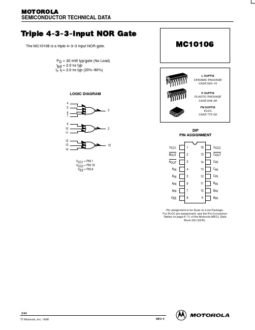
VCC1 BOUT 1 2 3 4 5 6 7 8 16 15 14 13 12 11 10 9 VCC2 COUT CIN CIN CIN BIN BIN BIN
15
VCC1 = PIN 1 VCC2 = PIN 16 VEE = PIN 8
AOUT AIN AIN AIN AIN VEE
Pin assignment is for Dual–in–Line Package. For PLCC pin assignment, see the Pin Conversion Tables on page 6–11 of the Motorola MECL Data Book (DL122/D).
Logic 1 Logic 0 Logic 1 Logic 0 (50Ω Load)
VOH VOL VOHA VOLA
(20 to 80%) (20 to 80%)
ELECTRICAL CHARACTERISTICS (continued)
TEST VOLTAGE VALUES (Volts) @ Test Temperature –30°C +25°C +85°C Pin Under Test 8 4 4 3 2 3 2 3 2 3 2 4 9 Pulse In t4+3– t4–3+ (20 to 80%) t3+ 3 3 3 4 4 4 Pulse Out 3 3 3 4 9 4 9 4 4 VIHmax –0.890 –0.810 –0.700 VILmin –1.890 –1.850 –1.825 VIHAmin –1.205 –1.105 –1.035 VILAmax –1.500 –1.475 –1.440 VEE –5.2 –5.2 –5.2 (VCC) Gnd 1, 16 1, 16 1, 16 1, 16 1, 16 1, 16 1, 16 1, 16 1, 16 1, 16 1, 16 +2.0 V 1, 16 1, 16 1, 16
STPS40H100CW;中文规格书,Datasheet资料
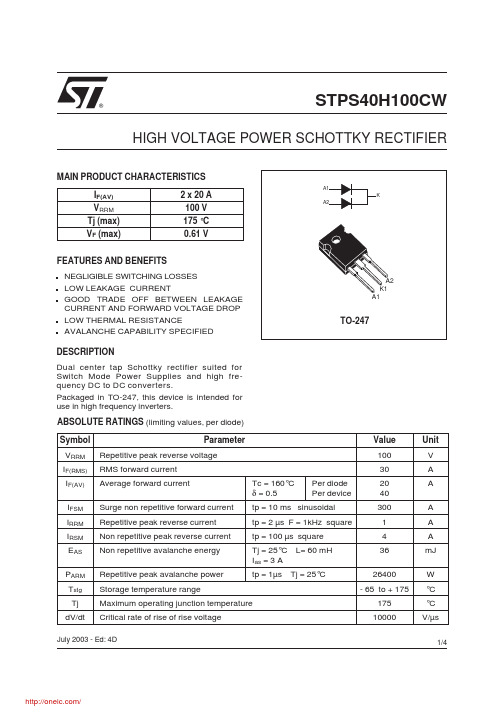
A2 K1 A1
TO-247
DESCRIPTION Dual center tap Schottky rectifier suited for Switch Mode Power Supplies and high frequency DC to DC converters. Packaged in TO-247, this device is intended for use in high frequency inverters. ABSOLUTE RATINGS (limiting values, per diode) Symbol VRRM IF(RMS) IF(AV) IFSM IRRM IRSM EAS PARM Tstg Tj dV/dt RMS forward current Average forward current Surge non repetitive forward current Repetitive peak reverse current Non repetitive peak reverse current Non repetitive avalanche energy Repetitive peak avalanche power Storage temperature range Maximum operating junction temperature Critical rate of rise of rise voltage Tc = 160°C δ = 0.5 Per diode Per device Parameter Repetitive peak reverse voltage Value 100 30 20 40 300 1 4 36 26400 - 65 to + 175 175 10000 Unit V A A A A A mJ W °C °C V/µs
MC100EP101FAR2G,MC10EP101FAR2G,MC100EP101MNR4G,MC10EP101MNR4G,MC10EP101MNG, 规格书,Datasheet 资料

MC10EP101, MC100EP101 3.3V / 5V ECL Quad 4−Input OR/NORDescriptionThe MC10/100EP101 is a Quad 4−input OR/NOR gate. The device is functionally equivalent to the E101. With AC performance faster than the E101 device, the EP101 is ideal for applications requiring the fastest AC performance available.The 100 Series contains temperature compensation.Features•250 ps Typical Propagation Delay•Maximum Frequency > 3 GHz Typical•PECL Mode Operating Range: V CC = 3.0 V to 5.5 Vwith V EE = 0 V•NECL Mode Operating Range: V CC = 0 Vwith V EE = −3.0 V to −5.5 V•Open Input Default State•Pb−Free Packages are Available**For additional information on our Pb−Free strategy and soldering details, please download the ON Semiconductor Soldering and Mounting Techniques Reference Manual, SOLDERRM/D.See detailed ordering and shipping information in the package dimensions section on page 7 of this data sheet.ORDERING INFORMATIONNCV EE D3d D3c V CC D3b D3a D2d V CCV CC Q0Q0V EE D0a D0b D0c Figure 1. 32−Lead LQFP Pinout (Top View)Warning: All V CC and V EE pins must be externally connected to Power Supply to guarantee proper operation.Q 0Q 0Q 1Q 1Q 2Q 2Q 3Q 3NC 2526272829303132151413121110912345678242322212019181716V EE D3d D3c V CC D3b D3a D2dV CC V CC Q0Q0V EE D0a D0b D0c V CCQ2V CC D2cD2b D2a D1d D1c D1bD0d D1a Q1Q2Q3Q3Q1MC10EP101MC100EP101Figure 2. 32−Lead QFN Pinout (Top View)Table 3. ATTRIBUTESCharacteristics Value Internal Input Pulldown Resistor75 k W Internal Input Pullup Resistor N/AESD Protection Human Body ModelMachine ModelCharged Device Model > 4 kV > 100 V > 2 kVMoisture Sensitivity, Indefinite Time Out of Drypack (Note 1)Pb Pkg Pb−Free PkgLQFP−32 QFN−32Level 2Level 2Level 1Flammability Rating Oxygen Index: 28 to 34UL−94 V−0 @ 0.125 inTransistor Count173 DevicesMeets or exceeds JEDEC Spec EIA/JESD78 IC Latchup Test1.For additional information, see Application Note AND8003/D.Table 4. MAXIMUM RATINGSSymbol Parameter Condition 1Condition 2Rating Unit V CC PECL Mode Power Supply V EE = 0 V6V V EE NECL Mode Power Supply V CC = 0 V−6VV I PECL Mode Input VoltageNECL Mode Input Voltage V EE = 0 VV CC = 0 VV I≤ V CCV I≤ V EE6−6VVI out Output Current ContinuousSurge 50100mAmAI BB V BB Sink/Source± 0.5mA T A Operating Temperature Range−40 to +85°C T stg Storage Temperature Range−65 to +150°Cq JA Thermal Resistance (Junction−to−Ambient)0 lfpm500 lfpm 32 LQFP32 LQFP8055°C/W°C/Wq JC Thermal Resistance (Junction−to−Case)Standard32 LQFP12 to 17°C/Wq JA Thermal Resistance (Junction−to−Ambient)0 lfpm500 lfpm QFN−32QFN−323127°C/W°C/Wq JC Thermal Resistance (Junction−to−Case)2S2P QFN−3212°C/WT sol Wave Solder PbPb−Free 265265°CRecommended Operating Conditions is not implied. Extended exposure to stresses above the Recommended Operating Conditions may affect device reliability.Symbol Characteristic Min Typ Max Min Typ Max Min Typ Max Unit I EE Power Supply Current455775455875455975mA V OH Output HIGH Voltage (Note 3)216522902415223023552480229024152540mV V OL Output LOW Voltage (Note 3)136514901615143015551680149016151740mV V IH Input HIGH Voltage (Single−Ended)209024152155248022152540mV V IL Input LOW Voltage (Single−Ended)136516901460175514901815mV I IH Input HIGH Current150150150m AI IL Input LOW Current−150−150−150m A NOTE:Device will meet the specifications after thermal equilibrium has been established when mounted in a test socket or printed circuit board with maintained transverse airflow greater than 500 lfpm. Electrical parameters are guaranteed only over the declaredoperating temperature range. Functional operation of the device exceeding these conditions is not implied. Device specification limit values are applied individually under normal operating conditions and not valid simultaneously.2.Input and output parameters vary 1:1 with V CC. V EE can vary +0.3 V to −2.2 V.3.All loading with 50 W to V CC− 2.0 V.Table 6. 10EP DC CHARACTERISTICS, PECL V CC= 5.0 V, V EE = 0 V (Note 4)−40°C25°C85°CSymbol Characteristic Min Typ Max Min Typ Max Min Typ Max Unit I EE Power Supply Current455775455875455975mA V OH Output HIGH Voltage (Note 5)386539904115393040554180399041154240mV V OL Output LOW Voltage (Note 5)306531903315313032553380319033153440mV V IH Input HIGH Voltage (Single−Ended)379041153855418039154240mV V IL Input LOW Voltage (Single−Ended)306533903130345531903515mV I IH Input HIGH Current150150150m AI IL Input LOW Current−150−150−150m A NOTE:Device will meet the specifications after thermal equilibrium has been established when mounted in a test socket or printed circuit board with maintained transverse airflow greater than 500 lfpm. Electrical parameters are guaranteed only over the declaredoperating temperature range. Functional operation of the device exceeding these conditions is not implied. Device specification limit values are applied individually under normal operating conditions and not valid simultaneously.4.Input and output parameters vary 1:1 with V CC. V EE can vary +2.0 V to −0.5 V.5.All loading with 50 W to V CC− 2.0 V.Table 7. 10EP DC CHARACTERISTICS, NECL V CC = 0 V, V EE= −5.5 V to −3.0 V (Note 6)−40°C25°C85°CSymbol Characteristic Min Typ Max Min Typ Max Min Typ Max Unit I EE Power Supply Current455775455875455975mA V OH Output HIGH Voltage (Note 7)−1135−1010−885−1070−945−820−1010−885−760mV V OL Output LOW Voltage (Note 7)−1935−1810−1685−1870−1745−1620−1810−1685−1560mV V IH Input HIGH Voltage (Single−Ended)−1210−885−1145−820−1085−760mV V IL Input LOW Voltage (Single−Ended)−1935−1610−1870−1545−1810−1485mV I IH Input HIGH Current150150150m AI IL Input LOW Current−150−150−150m A NOTE:Device will meet the specifications after thermal equilibrium has been established when mounted in a test socket or printed circuit board with maintained transverse airflow greater than 500 lfpm. Electrical parameters are guaranteed only over the declaredoperating temperature range. Functional operation of the device exceeding these conditions is not implied. Device specification limit values are applied individually under normal operating conditions and not valid simultaneously.6.Input and output parameters vary 1:1 with V.Symbol Characteristic Min Typ Max Min Typ Max Min Typ Max Unit I EE Power Supply Current405575405875456085mA V OH Output HIGH Voltage (Note 9)215522802405215522802405215522802405mV V OL Output LOW Voltage (Note 9)135514801605135514801605135514801605mV V IH Input HIGH Voltage (Single−Ended)207524202075242020752420mV V IL Input LOW Voltage (Single−Ended)135516751355167513551675mV I IH Input HIGH Current150150150m AI IL Input LOW Current−150−150−150m A NOTE:Device will meet the specifications after thermal equilibrium has been established when mounted in a test socket or printed circuit board with maintained transverse airflow greater than 500 lfpm. Electrical parameters are guaranteed only over the declaredoperating temperature range. Functional operation of the device exceeding these conditions is not implied. Device specification limit values are applied individually under normal operating conditions and not valid simultaneously.8.Input and output parameters vary 1:1 with V CC. V EE can vary +0.3 V to −2.2 V.9.All loading with 50 W to V CC− 2.0 V.Table 9. 100EP DC CHARACTERISTICS, PECL V CC= 5.0 V, V EE = 0 V (Note 10)−40°C25°C85°CSymbol Characteristic Min Typ Max Min Typ Max Min Typ Max Unit I EE Power Supply Current405875406175456485mA V OH Output HIGH Voltage (Note 11)385539804105385539804105385539804105mV V OL Output LOW Voltage (Note11)305531803305305531803305305531803305mV V IH Input HIGH Voltage (Single−Ended)377541203775412037754120mV V IL Input LOW Voltage (Single−Ended)305533753055337530553375mV I IH Input HIGH Current150150150m AI IL Input LOW Current−150−150−150m A NOTE:Device will meet the specifications after thermal equilibrium has been established when mounted in a test socket or printed circuit board with maintained transverse airflow greater than 500 lfpm. Electrical parameters are guaranteed only over the declaredoperating temperature range. Functional operation of the device exceeding these conditions is not implied. Device specification limit values are applied individually under normal operating conditions and not valid simultaneously.10.Input and output parameters vary 1:1 with V CC. V EE can vary +2.0 V to −0.5 V.11.All loading with 50 W to V CC− 2.0 V.Table 10. 100EP DC CHARACTERISTICS, NECL V CC = 0 V, V EE= −5.5 V to −3.0 V (Note 12)−40°C25°C85°CSymbol Characteristic Min Typ Max Min Typ Max Min Typ Max UnitI EE Power Supply Current V CC = −3.3VV CC = −5.0 V 404055587575404058617575454560648585mAI EE Power Supply Current506380556785607088mA V OH Output HIGH Voltage (Note 13)−1145−1020−895−1145−1020−895−1145−1020−895mV V OL Output LOW Voltage (Note 13)−1945−1820−1695−1945−1820−1695−1945−1820−1695mV V IH Input HIGH Voltage (Single−Ended)−1225−880−1225−880−1225−880mV V IL Input LOW Voltage (Single−Ended)−1945−1625−1945−1625−1945−1625mV I IH Input HIGH Current150150150m AI IL Input LOW Current−150−150−150m A NOTE:Device will meet the specifications after thermal equilibrium has been established when mounted in a test socket or printed circuit board with maintained transverse airflow greater than 500 lfpm. Electrical parameters are guaranteed only over the declaredoperating temperature range. Functional operation of the device exceeding these conditions is not implied. Device specification limit values are applied individually under normal operating conditions and not valid simultaneously.12.Input and output parameters vary 1:1 with V.Table 11. AC CHARACTERISTICS V CC = 0 V; V EE = −3.0 V to −5.5 V or V CC = 3.0 V to 5.5 V; V EE = 0 V (Note 14)−40°C25°C 85°C Symbol CharacteristicMinTyp MaxMinTyp MaxMinTyp MaxUnit f max Maximum Frequency(See Figure 4. F max /JITTER)> 3> 3> 3GHz t PLH ,t PHL Propagation DelayD to Q, Q10100125180225280325380150200250300370400170250300320420450pst SKEW Within Device SkewQ, Q Device to Device Skew (Note 15)155020020502002050200ps t JITTER Cycle −to −Cycle Jitter(See Figure 4. F max /JITTER)0.2< 10.2< 10.2< 1ps t r t fOutput Rise/Fall Times Q, Q(20% − 80%)100150200120170220150190250psNOTE:Device will meet the specifications after thermal equilibrium has been established when mounted in a test socket or printed circuitboard with maintained transverse airflow greater than 500 lfpm. Electrical parameters are guaranteed only over the declaredoperating temperature range. Functional operation of the device exceeding these conditions is not implied. Device specification limit values are applied individually under normal operating conditions and not valid simultaneously.14.Measured using a 750 mV source, 50% duty cycle clock source. All loading with 50 W to V CC − 2.0 V.15.Skew is measured between outputs under identical transitions.1002003004005006007008009001000010002000300040005000Figure 4. F max /JitterFREQUENCY (MHz)V O U T p p (m V )Figure 5. Typical Termination for Output Driver and Device Evaluation V TTV TT = V CC − 2.0 VORDERING INFORMATIONDevice Package Shipping†MC10EP101FA LQFP−32250 Units / Tray MC10EP101FAG LQFP−32(Pb−Free)250 Units / Tray MC10EP101FAR2LQFP−322000 / Tape & ReelMC10EP101FAR2G LQFP−32(Pb−Free)2000 / Tape & Reel MC100EP101FA LQFP−32250 Units / TrayMC100EP101FAG LQFP−32(Pb−Free)250 Units / Tray MC100EP101FAR2LQFP−322000 / Tape & ReelMC100EP101FAR2G LQFP−32(Pb−Free)2000 / Tape & ReelMC10EP101MNGQFN−32(Pb−Free)74 Units / RailMC10EP101MNR4G1000 / Tape & ReelMC100EP101MNG74 Units / RailMC100EP101MNR4G1000 / Tape & Reel†For information on tape and reel specifications, including part orientation and tape sizes, please refer to our Tape and Reel Packaging Specifications Brochure, BRD8011/D.Resource Reference of Application NotesAN1405/D−ECL Clock Distribution TechniquesAN1406/D−Designing with PECL (ECL at +5.0 V)AN1503/D−ECLinPS t I/O SPiCE Modeling KitAN1504/D−Metastability and the ECLinPS FamilyAN1568/D−Interfacing Between LVDS and ECLAN1672/D−The ECL Translator GuideAND8001/D−Odd Number Counters DesignAND8002/D−Marking and Date CodesAND8020/D−Termination of ECL Logic DevicesAND8066/D−Interfacing with ECLinPSAND8090/D−AC Characteristics of ECL DevicesAET −U M0.20 (0.008)ZA C NOTES:1.DIMENSIONING AND TOLERANCING PER ANSI Y14.5M, 1982.2.CONTROLLING DIMENSION:MILLIMETER.3.DATUM PLANE −AB − IS LOCATED AT BOTTOM OF LEAD AND IS COINCIDENT WITH THE LEAD WHERE THE LEAD EXITS THE PLASTIC BODY AT THE BOTTOM OF THE PARTING LINE.4.DATUMS −T −, −U −, AND −Z − TO BE DETERMINED AT DATUM PLANE −AB −.5.DIMENSIONS S AND V TO BEDETERMINED AT SEATING PLANE −AC −.6.DIMENSIONS A AND B DO NOT INCLUDE MOLD PROTRUSION. ALLOWABLEPROTRUSION IS 0.250 (0.010) PER SIDE.DIMENSIONS A AND B DO INCLUDE MOLD MISMATCH AND AREDETERMINED AT DATUM PLANE −AB −.7.DIMENSION D DOES NOT INCLUDE DAMBAR PROTRUSION. DAMBARPROTRUSION SHALL NOT CAUSE THE D DIMENSION TO EXCEED 0.520 (0.020).8.MINIMUM SOLDER PLATE THICKNESS SHALL BE 0.0076 (0.0003).9.EXACT SHAPE OF EACH CORNER MAY VARY FROM DEPICTION.DIM A MIN MAX MIN MAX INCHES 7.000 BSC 0.276 BSC MILLIMETERS B 7.000 BSC 0.276 BSC C 1.400 1.6000.0550.063D 0.3000.4500.0120.018E 1.350 1.4500.0530.057F 0.3000.4000.0120.016G 0.800 BSC 0.031 BSC H 0.0500.1500.0020.006J 0.0900.2000.0040.008K 0.4500.7500.0180.030M 12 REF 12 REF N 0.0900.1600.0040.006P 0.400 BSC 0.016 BSC Q 1 5 1 5 R 0.1500.2500.0060.010V 9.000 BSC 0.354 BSC V1 4.500 BSC 0.177 BSC ______B1 3.500 BSC 0.138 BSC A1 3.500 BSC 0.138 BSC S 9.000 BSC 0.354 BSC S1 4.500 BSC 0.177 BSC W 0.200 REF 0.008 REF X1.000 REF 0.039 REF32 LEAD LQFP CASE 873A −02QFN32 5*5*1 0.5 P CASE 488AM −01ISSUE O2 X*For additional information on our Pb −Free strategy and soldering details, please download the ON Semiconductor Soldering and Mounting Techniques Reference Manual, SOLDERRM/D.ON Semiconductor and are registered trademarks of Semiconductor Components Industries, LLC (SCILLC). SCILLC reserves the right to make changes without further notice to any products herein. SCILLC makes no warranty, representation or guarantee regarding the suitability of its products for any particular purpose, nor does SCILLC assume any liability arising out of the application or use of any product or circuit, and specifically disclaims any and all liability, including without limitation special, consequential or incidental damages.“Typical” parameters which may be provided in SCILLC data sheets and/or specifications can and do vary in different applications and actual performance may vary over time. All operating parameters, including “Typicals” must be validated for each customer application by customer’s technical experts. SCILLC does not convey any license under its patent rights nor the rights of others. SCILLC products are not designed, intended, or authorized for use as components in systems intended for surgical implant into the body, or other applications intended to support or sustain life, or for any other application in which the failure of the SCILLC product could create a situation where personal injury or death may occur. Should Buyer purchase or use SCILLC products for any such unintended or unauthorized application, Buyer shall indemnify and hold SCILLC and its officers, employees, subsidiaries, affiliates,and distributors harmless against all claims, costs, damages, and expenses, and reasonable attorney fees arising out of, directly or indirectly, any claim of personal injury or death associated with such unintended or unauthorized use, even if such claim alleges that SCILLC was negligent regarding the design or manufacture of the part. SCILLC is an Equal Opportunity/Affirmative Action Employer. This literature is subject to all applicable copyright laws and is not for resale in any manner.PUBLICATION ORDERING INFORMATIONECLinPS is a trademark of Semiconductor Components INdustries, LLC (SCILLC).。
M100-2PT 4PT模拟量输出模块 说明书
M100-2PT/4PT模拟量输出模块用户手册感谢您使用MC100系列PLC。
在使用PLC 产品前,请您仔细阅读本手册,以便更清楚地掌握产品特性,更安全地应用,充分利用本产品丰富的功能。
本速查手册用于MC100 系列PLC的设计、安装、连接和维护的快速指引,便于用户现场查阅所需信息,并有相关选配件的简介,常见问题答疑等,便于参考。
本手册适合MC100系列以下成员:MC100-2PTMC100-4PT版本号:V1.2日期:2010.1.15编码:R29090039若需要更详细的产品资料,可参考我公司发行的《MC100系列可编程控制器用户手册》、《X-Builder编程软件用户手册》和《MC100/MC200系列可编程控制器编程参考手册》。
如需要,可向供货商咨询。
1. 外观以及部件名称图1-1 外观及部件图2. 安装说明2.1安装方法PLC须水平安装在电气柜的背板上,上下方向安装并保持PLC与上方和下方的设备或柜壁的距离不小于20cm。
其他方向安装均不利于PLC自身散热,为不合适安装方式。
⏹采用DIN槽安装固定在振动不大的环境下,可以采用35mm宽度的DIN槽进行安装。
打开模块底部的DIN卡扣,将模块底部卡在DIN导轨上;旋转模块贴近DIN导轨,合上DIN卡扣;仔细检查模块上DIN卡扣与DIN导轨是否紧密固定好,如下图:图2-1 导轨安装示意图⏹采用螺钉安装固定在振动较大的场合必须使用螺丝来固定,螺丝可选用M3,按照下图所示的尺寸进行定位、钻安装孔;用合适的螺钉将模块固定在背板上。
MC100系列特殊模块的外形尺寸与安装孔位尺寸如下图所示:图2-2 螺钉安装示意图2.2电缆连接及规格电缆规格在为PLC配线时,建议使用多股铜导线,并预制绝缘端头,这样可保证接线质量。
推荐选用导线的截面积和型号如下表所示。
将加工好的电缆头用螺丝固定在PLC的接线端子上,注意螺钉位置正确,螺钉的旋紧力矩在0.5~0.8Nm,保证可靠连接,又不致损坏螺丝。
CDRR94NP-100MC中文资料

1.7
0.75
3790-0014
15 CDRR94NP-47ØMC 470 47 μH ± 20% 435.0(348)
1.6
0.70
3790-0015
16 CDRR94NP-68ØMC 680 68 μH ± 20% 670.0(536)
1.3
0.55
3790-0016
17 CDRR94NP-82ØMC 820 82 μH ± 20% 898.0(718)
1-3. DIMENSION RECOMMENDED (mm)
STAMP・DATE CODE
7.1
DIRECTLY STAMP UNFIXED THE POSITION
2.COIL SPECIFICATION 2-1. CONNECTION (BOTTOM )
3.0
3.0
RoHS
compliance
和電流(A) 電流(A) スミダ
※3
※4
コード
(at 20℃) △T=40℃
10.8
5.0
3790-0019
20 CDRR94NP-1R5MB 1R5 1.5μH ± 20% 16.9(13.5)
9.6
4.5
3790-0020
21 CDRR94NP-2R2MB 2R2 2.2μH ± 20% 27.5(22.0)
DECREASES TO 10% LOWER OF IT'S INITIAL VALUE. ※4 TEMPERATURE RISE: THE VALUE OF D.C.CURRENT WHEN THE TEMPERATURE RISE IS △t=40℃(Ta=20℃).
元器件交易网
3.0
MC10H644FN中文资料

Q4 18 GT Q3 GT Q2 GT 19 20 1 2 3 4 Q1 MECL 10H is a trademark of Motorola, Inc.
11/93
VT 17
Q5 16
GT 15
R 14 13 12 11 10 9 VE DE VBB DE GE
The user has a choice of using either TTL or PECL (ECL referenced to FN SUFFIX +5.0V) for the input clock. TTL clocks are typically used in present MPU PLASTIC PACKAGE systems. However, as clock speeds increase to 50MHz and beyond, the CASE 775–02 inherent superiority of ECL (particularly differential ECL) as a means of clock signal distribution becomes increasingly evident. The H644 also uses differential ECL internally to achieve its superior skew characteristic. The H644 includes divide–by–two and divide–by–four stages, both to achieve the necessary duty cycle and skew to generate MPU clocks as required. A typical 50MHz processor application would use an input clock running at 100MHz, thus obtaining output clocks at 50MHz and 25MHz (see Logic Symbol). The 10H version is compatible with MECL 10H™ ECL logic levels, while the 100H version is compatible with 100K levels (referenced to +5.0V). Function
MC-IsoAmpPWRA20100样本KNICK(中文版)
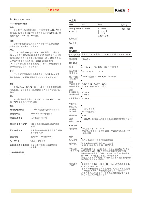
IsoAmp ®PWR201006mm knick IsoAmp PWR A 20100,6m m .DIP 420mA HART 6.1mm DIP 0...20mA 4...20mA0...10V DIP 4...20mA 6mm DIL 的电源中继器任务问题解决外形优势技术特点有效的电源供应 特别的单元 灵活和高精度 简单和快速的配置 低化费的安装五年质量保证期 高精度传送连接要达到好的隔离器特性会导系统的复杂,并化费金钱和占用空间。
公司的是第一个非常紧凑宽两线制传送电源中继器它高精度的传送能源和传送测量信号和输出的电气隔离。
通过转换你能在电源中继器上选择不同于到的输出信号。
信号保证信号传送无改变。
只有的宽度允许电源中继器使用在很小的空间里。
模块盒有可靠的结构并经过测试,只有宽带螺纹接线端。
转换使输出值的转换不需要打开盒子。
新的小尺寸电源中继器有着优秀的性能。
安全隔离和的精度允许使用在高要求的场合。
输出信号能被转换才、和。
通过转换选择已校准的范围。
无源信号的两线制传送外形的三通道隔离已校准信号可转换 用转换很容易转换并保护调整 错误测量供给电路和测量信号电气隔离 在一个单元中 安全隔离 传送 电源供应的十字连接 根据最在(根据协议)大量的平行电源中继器只需要一 次连线SMART HART 灵活和安全的二线制供应,传送器通过测量信号线,传送根据传送器数据协议或协议。
转变信号到或输出。
提供 4...20mA SMART HART 0...20mA 0...10V IsoAmp PWR A 201000.1%EN61140300V ®®®6mm 电源供应产品线输入数据输入()电流回路输出数据输出剩余波纹﹤10mV rms传送特征增益错误<测量值0.1%响应时间说明IsoAmp PWR A 20100®A20100F024V 直流4...20mA,0...20mA 0...10V 或已校准可选供应电压常量,电流最大限制值16.5V, 3...22mA 25mA 电源供应输入设备 定单号输出4...20mA 4...20mA 0...20mA 0...10V 已校准选择输出剩余波纹﹤10mV rms输入短路时输出信号22...25mA 11...12.5V或输入开路时输出信号<或输出及时的3m A 0...20mA 0...10V 0负载电流输出时≤(在时≤欧)10V 20mA 500电压输出时≤(在时≤欧)1mA 10V 10k 补偿电流输出时电压输出时<30A μ<30mV电流输出电压输出<测量值0.2%<5ms通信输出4...20mA 根据协议双向传送输出和电流回路的频移键控信号HART 电源供应24V 15%1W直流(±)约电源供应能经过一个设备到另一个设备中通过用十字接头连接电气隔离测试电压输入和输出/电源供应之间5kV交流输出和电源供应之间510V交流工作电压隔离输入、输出和电源供应三通道隔离在电流回路和输出电源供应之间最大右有的直流或交流按照的过压等级和污染等级在输出和电源供应之间最大可有的直流或交流按照的过压等级和污染等级应用在高压工作环境时,必须保证跟相邻设备有足够的空间或隔离和电冲击保护。
MC2的详细参数
特性
参数
量程
0 ~ 9999999 pulse
输入阻抗
>1Mohm
触发电平
-1~14V in 1V steps and open collector inputs
最小信号幅度
2Vpp(pulse length>50us),3Vpp(pulse length 10..50us)
开关量测试
特点
参数
0.01%FS+0.025%RDG
EXT100
EXT100-IS
0 to 10 MPa
0 to 100 bar
0.0001
0.001
0.005%FS+0.0125%RDG
0.01%FS+0.025%RDG
EXT160
EXT160-IS
0 to 16 MPa
0 to 160 bar
0.0001
0.001
0.01 mV
0.02% RDG + 0.1 mV
-3 ~ -0.25 V
0.1 mV
0.02% RDG + 0.1 mV
0.25 ~ 12 V
0.1 mV
0.02% RDG + 0.1 mV
特征
参数
温度系数
< ±0.0015% RDG /℃outside of 18 ~28℃
< ±0.0008% RDG /℉outside of 64.4 ~82.4℉
输入阻抗
<7.5ohm
可选单位
mA,µA
显示刷新率
3/秒
回路电源
特性
参数
输出电流
最大25mA,短路保护
输出电压
- 1、下载文档前请自行甄别文档内容的完整性,平台不提供额外的编辑、内容补充、找答案等附加服务。
- 2、"仅部分预览"的文档,不可在线预览部分如存在完整性等问题,可反馈申请退款(可完整预览的文档不适用该条件!)。
- 3、如文档侵犯您的权益,请联系客服反馈,我们会尽快为您处理(人工客服工作时间:9:00-18:30)。
MC10H640, MC100H640 68030/040 PECL to TTL Clock DriverDescriptionThe MC10H/100H640 generates the necessary clocks for the 68030, 68040 and similar microprocessors. It is guaranteed to meet the clock specifications required by the 68030 and 68040 in terms of part−to−part skew, within−part skew and also duty cycle skew.The user has a choice of using either TTL or PECL (ECL referenced to +5.0 V) for the input clock. TTL clocks are typically used in present MPU systems. However, as clock speeds increase to 50 MHz and beyond, the inherent superiority of ECL (particularly differential ECL) as a means of clock signal distribution becomes increasingly evident. The H640 also uses differential PECL internally to achieve its superior skew characteristic.The H640 includes divide−by−two and divide−by−four stages, both to achieve the necessary duty cycle skew and to generate MPU clocks as required. A typical 50 MHz processor application would use an input clock running at 100 MHz, thus obtaining output clocks at50 MHz and 25 MHz (see Logic Diagram).Features•Generates Clocks for 68030/040•Meets 030/040 Skew Requirements•TTL or PECL Input Clock•Extra TTL and PECL Power/Ground Pins •Asynchronous Reset•Single +5.0 V Supply•Pb−Free Packages are Available*FunctionReset (R): LOW on RESET forces all Q outputs LOW and all Q outputs HIGH.Power−Up:The device is designed to have the POS edges of the ÷ 2 and ÷ 4 outputs synchronized at power up.Select (SEL): LOW selects the ECL input source (DE/DE). HIGH selects the TTL input source (DT).The H640 also contains circuitry to force a stable state of the ECL input differential pair, should both sides be left open. In this case, the DE side of the input is pulled LOW, and DE goes HIGH.*For additional information on our Pb−Free strategy and soldering details, please download the ON Semiconductor Soldering and Mounting Techniques Reference Manual, SOLDERRM/D.MARKING DIAGRAM*xxx= 10 or 100A= Assembly LocationWL= Wafer LotYY= YearWW= Work WeekG=Pb−Free PackagePLCC−28FN SUFFIXCASE 776MCxxxH640GAWLYYWW1*For additional marking information, refer toApplication Note AND8002/D.See detailed ordering and shipping information in the package dimensions section on page 7 of this data sheet.ORDERING INFORMATION1VT VT Q1GT GT Q0VT GTGTQ4Q5VTSEL56789101125242322212019Q1Figure 1. Pinout: PLCC −28(Top View)V BB DE DE VE R GE DTQ0VT VT Q3GT GT Q243228272618171615141312Figure 2. Logic DiagramTTL OutputsV BB DE DTSELRDE Q0Q1Q2Q3Q0Q4Q5Table 1. PIN DESCRIPTIONPIN FUNCTIONGT VT VE GE DE, DE V BB DT Qn, Qn SEL RTTL Ground (0 V)TTL V CC (+5.0 V)ECL V CC (+5.0 V)ECL Ground (0 V)ECL Signal Input (positive ECL)V BB Reference Output TTL Signal Input Signal Outputs (TTL)Input Select (TTL)Reset (TTL)Table 2. DC CHARACTERISTICS (V T = V E = 5.0 V ± 5%)Symbol CharacteristicCondition 0°C25°C 85°C MinMax MinMax MinMax Unit I EE Power Supply CurrentECL VE Pin 575757mA I CCH TTLTotal all VT pins303030mA I CCL303030mANOTE:Device will meet the specifications after thermal equilibrium has been established when mounted in a test socket or printed circuitboard with maintained transverse airflow greater than 500 lfpm. Electrical parameters are guaranteed only over the declaredoperating temperature range. Functional operation of the device exceeding these conditions is not implied. Device specification limit values are applied individually under normal operating conditions and not valid simultaneously.Table 3. 10H PECL DC CHARACTERISTICS (V T = V E = 5.0 V ± 5%)Symbol Characteristic Condition0°C25°C85°CUnit Min Max Min Max Min MaxI INH I INL Input HIGH CurrentInput LOW Current0.52550.51750.5175m AV IH1 V IL1Input HIGH VoltageInput LOW VoltageV E = 5.0 V 3.833.054.163.523.873.054.193.523.943.054.283.555VV BB1Output Reference Voltage 3.62 3.73 3.65 3.75 3.69 3.81V NOTE:Device will meet the specifications after thermal equilibrium has been established when mounted in a test socket or printed circuit board with maintained transverse airflow greater than 500 lfpm. Electrical parameters are guaranteed only over the declaredoperating temperature range. Functional operation of the device exceeding these conditions is not implied. Device specification limit values are applied individually under normal operating conditions and not valid simultaneously.1.PECL levels are referenced to V CC and will vary 1:1 with the power supply. The values shown are for V CC = 5.0V.Table 4. 100H PECL DC CHARACTERISTICS (V T = V E = 5.0 V ± 5%)Symbol Characteristic Condition0°C25°C85°CUnit Min Max Min Max Min MaxI INH I INL Input HIGH CurrentInput LOW Current0.52550.51750.5175m AV IH2 V IL2Input HIGH VoltageInput LOW VoltageV E = 5.0 V 3.8353.194.123.5253.8353.194.123.5253.8353.194.123.525VV BB2Output Reference Voltage 3.62 3.74 3.62 3.74 3.62 3.74V NOTE:Device will meet the specifications after thermal equilibrium has been established when mounted in a test socket or printed circuit board with maintained transverse airflow greater than 500 lfpm. Electrical parameters are guaranteed only over the declaredoperating temperature range. Functional operation of the device exceeding these conditions is not implied. Device specification limit values are applied individually under normal operating conditions and not valid simultaneously.2.PECL levels are referenced to V CC and will vary 1:1 with the power supply. The values shown are for V CC = 5.0V.Table 5. TTL DC CHARACTERISTICS (V T = V E = 5.0 V ± 5%)Symbol Characteristic Condition0°C25°C85°CUnit Min Max Min Max Min MaxV IH V IL Input HIGH VoltageInput LOW Voltage2.00.82.00.82.00.8VI IH Input HIGH Current V IN = 2.7 VV IN = 7.0 V 201002010020100m AI IL Input LOW Current V IN = 0.5 V−0.6−0.6−0.6mAV OH Output HIGH Voltage I OH = −3.0 mAI OH = −15 mA 2.52.02.52.02.52.0VV OL Output LOW Voltage I OL = 24 mA0.50.50.5VV IK Input Clamp Voltage I IN = −18 mA−1.2−1.2−1.2VI OS Output Short Circuit Current V OUT = 0 V−100−225−100−225−100−225mA NOTE:Device will meet the specifications after thermal equilibrium has been established when mounted in a test socket or printed circuit board with maintained transverse airflow greater than 500 lfpm. Electrical parameters are guaranteed only over the declaredoperating temperature range. Functional operation of the device exceeding these conditions is not implied. Device specification limit values are applied individually under normal operating conditions and not valid simultaneously.Table 6. AC CHARACTERISTICS (V T = V E = 5.0 V ± 5%)Symbol Characteristic Condition0°C25°C85°CUnit Min Max Min Max Min Maxt PLH Propagation Delay ECLD to OutputQ0 − Q3CL = 25 pF 4.0 6.0 4.0 6.0 4.2 6.2nst PLH Propagation Delay TTLD to OutputCL = 25 pF 4.0 6.0 4.0 6.0 4.3 6.3ns tskwd*Within−Device Skew CL = 25 pF0.50.50.5nst PLH Propagation Delay ECLD to OutputQ0, Q1CL = 25 pF 4.0 6.0 4.0 6.0 4.2 6.2nst PLH Propagation Delay TTLD to OutputCL = 25 pF 4.0 6.0 4.0 6.0 4.3 6.3nst PLH Propagation Delay ECLD to OutputQ4, Q5CL = 25 pF 4.0 6.0 4.0 6.0 4.2 6.2nst PLH Propagation Delay TTLD to OutputCL = 25 pF 4.0 6.0 4.0 6.0 4.3 6.3nst PD Propagation DelayR to OutputAll Outputs CL = 25 pF 4.3 6.3 4.3 6.3 5.07.0nst R t F Output Rise/Fall Time0.8 V to 2.0 VAll Outputs CL = 25 pF 2.52.52.52.52.52.5nsf max Maximum Input Frequency CL = 25 pF135135135MHz t pw Minimum Pulse Width 1.50 1.50 1.50ns t rr Reset Recovery Time 1.25 1.25 1.25ns NOTE:Device will meet the specifications after thermal equilibrium has been established when mounted in a test socket or printed circuit board with maintained transverse airflow greater than 500 lfpm. Electrical parameters are guaranteed only over the declaredoperating temperature range. Functional operation of the device exceeding these conditions is not implied. Device specification limit values are applied individually under normal operating conditions and not valid simultaneously.3.Within−Device Skew defined as identical transitions on similar paths through a device.Table 7. V CC and C L RANGES TO MEET DUTY CYCLE REQUIREMENTS(0°C ≤ T A≤ 85°C Output Duty Cycle Measured Relative to 1.5 V)Symbol Characteristic Condition Min Nom Max UnitRange of V CC and CL to meet mini-mum pulse width(HIGH or LOW)= 11.5 ns at f out≤ 40 MHz V CCCLQ0 − Q3Q0 − Q14.75105.0 5.2550VpFRange of V CC and CL to meet mini-mum pulse width(HIGH or LOW)= 9.5 ns at 40 < f out≤ 50 MHz V CCCLQ0 − Q3 4.875155.0 5.12527VpF10119P W (n s )Figure 3. Positive Pulse Width at 25°C Ambient and 50 MHz OutLOAD (pF)10119Figure 4. Negative Pulse Width at 25°C Ambient and 50 MHz OutLOAD (pF)N E G A T I V E P U L S E W I D T H (n s )10119P O S I T I V E P U L S E W I D T H (n s )10119Figure 7. Temperature versus Positive Pulse Widthfor 100H640 at 50 MHz and V CC = +5.0 V TEMPERATURE (°C)P O S I T I V E P U L S E W I D T H (n s )0°25°Figure 8. Temperature versus Negative Pulse Widthfor MC100H640 @ 50 MHz and V CC = +5.0 VTEMPERATURE (°C)10/100H640DUTY CYCLE CONTROLTo maintain a duty cycle of ± 5% at 50MHz, limit the load capacitance and/or power supply variation as shown in Figures 3and 4. For a ± 2.5% duty cycle limit, see Figures 5 and 6. Figures 7 and 8 show duty cycle variation with temperature. Figure 9shows typical TPD versus load. Figure 10 shows reset recovery time. Figure 11 shows output states after power up.Best duty cycle control is obtained with a single m P load and minimum line length.Figure 10. MC10H/100H640 Clock Phase and Reset Recovery Time After Reset PulseDT RESET, RQ0, Q1Q4, Q5Figure 11. Output Timing DiagramAFTER POWER UPOUTPUTS Q 4 & Q 5 WILL SYNC WITH POSITIVE EDGES OF D in & Q 0 → Q 3 & NEGATIVE EDGES OF Q 0 & Q 1D inQ 0 → Q 3Q 1 → Q 2Q 4 & Q 5ORDERING INFORMATIONDevice Package Shipping†MC10H640FN PLCC−2837 Units / Rail37 Units / RailMC10H640FNG PLCC−28(Pb−Free)MC10H640FNR2PLCC−28500 / Tape & Reel500 / Tape & ReelMC10H640FNR2G PLCC−28(Pb−Free)MC100H640FN PLCC−2837 Units / Rail37 Units / RailMC100H640FNG PLCC−28(Pb−Free)MC100H640FNR2PLCC−28500 / Tape & Reel500 / Tape & ReelMC100H640FNR2G PLCC−28(Pb−Free)†For information on tape and reel specifications, including part orientation and tape sizes, please refer to our Tape and Reel Packaging Specifications Brochure, BRD8011/D.Resource Reference of Application NotesAN1405/D−ECL Clock Distribution TechniquesAN1406/D−Designing with PECL (ECL at +5.0 V)AN1503/D−ECLinPS t I/O SPiCE Modeling KitAN1504/D−Metastability and the ECLinPS FamilyAN1568/D−Interfacing Between LVDS and ECLAN1672/D−The ECL Translator GuideAND8001/D−Odd Number Counters DesignAND8002/D−Marking and Date CodesAND8020/D−Termination of ECL Logic DevicesAND8066/D−Interfacing with ECLinPSAND8090/D−AC Characteristics of ECL DevicesPACKAGE DIMENSIONSPLCC −28FN SUFFIXPLASTIC PLCC PACKAGECASE 776−02ISSUE ESL−M S 0.010 (0.250) NST VIEW SNOTES:1.DATUMS −L−, −M−, AND −N− DETERMINED WHERE TOP OF LEAD SHOULDER EXITS PLASTIC BODY AT MOLD PARTING LINE.2.DIMENSION G1, TRUE POSITION TO BEMEASURED AT DATUM −T−, SEATING PLANE.3.DIMENSIONS R AND U DO NOT INCLUDE MOLD FLASH. ALLOWABLE MOLD FLASH IS 0.010 (0.250) PER SIDE.4.DIMENSIONING AND TOLERANCING PER ANSI Y14.5M, 1982.5.CONTROLLING DIMENSION: INCH.6.THE PACKAGE TOP MAY BE SMALLER THAN THE PACKAGE BOTTOM BY UP TO 0.012(0.300). DIMENSIONS R AND U ARE DETERMINED AT THE OUTERMOST EXTREMES OF THE PLASTIC BODY EXCLUSIVE OF MOLD FLASH, TIE BAR BURRS, GATE BURRS AND INTERLEAD FLASH, BUT INCLUDING ANY MISMATCH BETWEEN THE TOP AND BOTTOM OF THE PLASTIC BODY.7.DIMENSION H DOES NOT INCLUDE DAMBAR PROTRUSION OR INTRUSION. THE DAMBAR PROTRUSION(S) SHALL NOT CAUSE THE H DIMENSION TO BE GREATER THAN 0.037(0.940). THE DAMBAR INTRUSION(S) SHALL NOT CAUSE THE H DIMENSION TO BE SMALLER THAN 0.025 (0.635).DIM MIN MAX MIN MAX MILLIMETERSINCHES A 0.4850.49512.3212.57B 0.4850.49512.3212.57C 0.1650.180 4.20 4.57E 0.0900.110 2.29 2.79F 0.0130.0190.330.48G 0.050 BSC 1.27 BSC H 0.0260.0320.660.81J 0.020−−−0.51−−−K 0.025−−−0.64−−−R 0.4500.45611.4311.58U 0.4500.45611.4311.58V 0.0420.048 1.07 1.21W 0.0420.048 1.07 1.21X 0.0420.056 1.07 1.42Y −−−0.020−−−0.50Z 2 10 2 10 G10.4100.43010.4210.92K10.040−−− 1.02−−−____ON Semiconductor and are registered trademarks of Semiconductor Components Industries, LLC (SCILLC). SCILLC reserves the right to make changes without further notice to any products herein. SCILLC makes no warranty, representation or guarantee regarding the suitability of its products for any particular purpose, nor does SCILLC assume any liability arising out of the application or use of any product or circuit, and specifically disclaims any and all liability, including without limitation special, consequential or incidental damages.“Typical” parameters which may be provided in SCILLC data sheets and/or specifications can and do vary in different applications and actual performance may vary over time. All operating parameters, including “Typicals” must be validated for each customer application by customer’s technical experts. SCILLC does not convey any license under its patent rights nor the rights of others. SCILLC products are not designed, intended, or authorized for use as components in systems intended for surgical implant into the body, or other applications intended to support or sustain life, or for any other application in which the failure of the SCILLC product could create a situation where personal injury or death may occur. Should Buyer purchase or use SCILLC products for any such unintended or unauthorized application, Buyer shall indemnify and hold SCILLC and its officers, employees, subsidiaries, affiliates,and distributors harmless against all claims, costs, damages, and expenses, and reasonable attorney fees arising out of, directly or indirectly, any claim of personal injury or death associated with such unintended or unauthorized use, even if such claim alleges that SCILLC was negligent regarding the design or manufacture of the part. SCILLC is an Equal Opportunity/Affirmative Action Employer. This literature is subject to all applicable copyright laws and is not for resale in any manner.PUBLICATION ORDERING INFORMATIONECLinPS is a trademark of Semiconductor Components Industries, LLC (SCILLC).MECL 10H is a trademark of Motorola, Inc.。