ATmega32L-8AU中文资料
ATmega8寄存器资料整理

ATmega8寄存器资料整理ATmega8各模塊及相關寄存器功能ADC模塊1.ADMUX--ADC多路選擇寄存器:REFS1,REFS0: = 0,0 關閉內部的參考電壓0,1 Avcc利用AREF腳的外接電容1,0 保留1,1 開啟內部的2.56V參考電壓, AREF腳外接電容.ADLAR: = 1對ADC轉換結果進行左調節, = 0對ADC轉換結果進行右調節,詳見IC spec,我要ADLAR=0.MUX3~0: =0000~0111分別選擇ADC0~ADC7作為輸入, =1110 1.23V(VBG), =1111 0V(GND).2.ADCSR--ADC控制和狀態寄存器ADEN: ADC使能ADSC: ADC工作于單次模式時,’ADSC=1’啟動一次轉換,轉換結束后ADSC由硬件清0.ADC工作于連續模式時,’ADSC=1’啟動轉換,只需一次.對該位寫0沒有意義.注意:每一次對該位寫’1’都會有一次啞轉換.ADFR: =1選擇ADC連續模式. =0則終止連續模式.ADIF: ADC中斷標識位.執行中斷程序后由硬件清0,對該位寫’1’也可以將其清0ADIE:ADC中斷使能.ADPS2..ADPS0: =000~111時ADC的分頻系數分別為2,2,4,8,16,32,64,1283. ADCH/ADCL:ADC結果數據寄存器,讀取時要先讀ADCL.USART模塊1.UDR--USART數據接收/發射寄存器.2.UCSRA--USART控制和狀態寄存器A.RXC: 接收數據完成標識位, RXC在读UDR时自动被清除, 如果采用中断方式则中断例程必须读一次UDR.TXC: 發送數據結束標識位, TXC 置位表示数据已经从发送移位寄存器发送出去且UDR 中没有新的要发送的数据,在半双工通信应用中,由于发送器在发送完数据之后要立即转换到接收模式,所以这个标志位特别有用.如果TXCIE 已置位则TXC 置位将引发发送结束中断,进入中断例程后TXC 自动清零,或者用户可以对其写1清零. UDRE: UART数据寄存器空当数据从UDR 传送到发送移位寄存器后,UDRE 置位,表明发送器已经准备好接收新的要发送的数据.当UDRIE 置位,则只要UDRE 为’1’, UART 发送结束中断就可以执行.写UDR 将复位UDRE. 如果利用中断方式发送数据,则在UART 数据寄存器空中断例程里必须写UDR 以清除UDRE, 否则中断将连续发生.复位后UDRE 的初始值为’1’, 表明发送器就绪.FE: 接收帧错误標識位,MCU 检测到帧错误如检测到停止位为0 时FE 置位,当检测到数据停止位为1 时FE 复位.讀接收緩沖器清除該標識.DOR: 數據過速標識位, 如果UDR 未读而新接收的数据又已进入移位寄存器,则OR 置位. 讀接收緩沖器清除該標識. PE: (?UPE)接收數據奇偶校驗錯誤標識位,讀接收緩沖器清除該標識.U2X: 對異步通訊, U2X=1時波特率加倍.對同步通訊,該位無效,必須寫0.MPCM: =1時為多處理器通訊模式,在該模式下,接收到的未包含地址的楨數據被忽略,不影響發送數據.3.UCSRB-- USART控制和狀態寄存器B.RXCIE: 接收結束中斷使能.TXCIE: 發送結束中斷使能.UDRIE: 數據寄存器空中斷使能.RXEN: =1時接收使能.同時自動設置RXD引腳為接收腳.接收禁能將導致TXC/DOR/FE無法置位,同時也不能復位已經置位的標識位.TXEN: =1時接收接收.同時自動設置TXD引腳為發送腳.UCSZ2: 與UCSRC中的UCSZ1/UCSZ0位一起決定接收和發送數據的楨格式(8/9/10位)RXB8/TXB8: 接收/發送數據的第9位.4. UCSRC-- USART控制和狀態寄存器C.(UCSRC與UBRRH共用一個IO地址)URSEL: =1時讀/寫UCSRC寄存器,=0時讀/寫UBRRH寄存器.UMSEL: =1選擇UART, =0選擇USARTUPM1..UPM0: =0, 0 禁止奇偶校驗,=0,1 保留, =1,0 使能偶校驗, =1,1 使能奇校驗.USBS: =0 發送1位停止位, =1 發送2位停止位. 該位的設置與接收無關.UCSZ1..UCSZ0: 與UCSZ2一起決定數據楨的位數UCSZ2..UCSZ0 = 0,0,0~0,1,1 分別為5/6/7/8位.= 1,0,0~1,1,0 保留= 1,1,1 9位(復位后的缺省值為0,1,1即8位)UCPOL: =0 在時鐘脈沖的上升沿發送一位數據,下降沿接收一位數據. =1則反之.5.UBRRH/UBRRL: UBRRH的低4位和UBRRL組成12位波特率寄存器.(見IC spec.)WDT模塊1.WDTCR—看門狗定時器控制寄存器WDCE: 看門狗關閉使能.WDE: =1使能看門狗.關閉看門狗的步驟為: 1. 在同一个指令内对WDCE 和WDE 写逻辑1,即使WDE 已经为12. 在4 个时钟之内对WDE 写逻辑0WDP2..WDP0: 選擇WDT的溢出時間.TWI模塊1.TWBR—TWI位傳輸率寄存器.SCL頻率=CPU時鐘/(16+2*TWBR*4TWPS)主機模式下要求TWBR>10.2.TWCR—TWI控制寄存器TWINT: TWI中斷標識位該位必須由軟件清0.另外清0該位時會啟動TWI,因此清0該位之前需先設置好TWAR/TWSR/TWDR TWEA: TWI應答信號時能.TWSTA: TWI啟動條件位. 該位置’1’時向總線發送一個啟動信號,然后該位要用軟件清0.TWSTO: TWI停止條件位. 該位置’1’時向總線發送一個停止信號,然后該位自動清0.TWWC: TWI寫沖突標識位. 當TWIBT=0時寫TWDR,該位置位; 當TWIBT=1時寫TWDR,該位清0. TWEN: TWI使能位. 只要將該位置’1’,TWI就對SDA和SCL腳具有控制權.TWIE: TWI中斷使能.3.TWSR—TWI狀態寄存器.TWS7..TWS3: 指示TWI的狀態.TWPS1..TWPS0: 位傳輸速率的預分頻值. =0,0~1,1對應的預分頻值分別為1,4,16,644.TWDR-- TWI數據寄存器.5.TWAR: TWI(slave) 地址寄存器.TWA6..TWA0: TWI(slave) 地址TWGCE: TWI通用呼叫識別使能位.T0模塊1.TIMSK—T/C中斷屏蔽寄存器TOIE0: T/C0溢出中斷使能.2.TIFR—T/C中斷標識寄存器.TOV0: T/C0溢出中斷標識位.3.TCCR0--T/C控制寄存器.CS02…CS00: = 0,0,0 T/C停止.=0,0,1~1,0,1 時鐘分別為I/O時鐘, I/O時鐘/8, I/O時鐘/64, I/O 時鐘/256, I/O時鐘/1024,=1,1,0 T0腳的時鐘,下降沿=1,1,1 T0腳的時鐘,上升沿4.TCNT0—T/C計數寄存器.T1模塊1. TIMSK—T/C中斷屏蔽寄存器TICIE1: T/C1輸入捕獲中斷使能.OCIE1A: T/C1輸出比較匹配A中斷使能.OCIE1B: T/C1輸出比較匹配B中斷使能.TOIE1: T/C1溢出中斷使能.2.TIFR—T/C中斷標識寄存器.ICF1: T/C1輸入捕獲中斷標識位.OCF1A: T/C1輸出比較匹配A中斷標識位.OCF1B: T/C1輸出比較匹配B中斷標識位.TOV1: T/C1溢出中斷標識位.3.TCCR1A—T/C1控制寄存器A./doc/4b8ab1dbce2f0066f533228e.html1A0(/doc/4b8ab1dbce2f0066f533228e.html1B0): 决定T/C1 的比较匹配发生时输出引脚OC1A(OC1B)的动作,對I/O口的控制權最高,相应的方向控制位要设置为1, 以便将其配置为输出.WGM13..0=正常模式或CTC模式時:/doc/4b8ab1dbce2f0066f533228e.html1A0(/doc/4b8ab1dbce2f0066f533228e.html1B0): =0,0 T/C1與输出引脚OC1A(OC1B)斷開=0,1 比较匹配发生时OC1A(OC1B) 輸出反相.=1,0 比较匹配发生时OC1A(OC1B)=0; OC1A(OC1B)=1 at TOP =1,1 比较匹配发生时OC1A(OC1B)=1; OC1A(OC1B)=0 at TOPWGM13..0=快速PWM模式時:/doc/4b8ab1dbce2f0066f533228e.html1A0(/doc/4b8ab1dbce2f0066f533228e.html1B0): =0,0 T/C1與输出引脚OC1A(OC1B)斷開=0,1 WGM13..0=15: 比较匹配发生时OC1A/OC1B反相輸出. OC1B斷開=1,0 比较匹配发生时OC1A(OC1B)=0; OC1A(OC1B)=1 at TOP =1,1 比较匹配发生时OC1A(OC1B)=1; OC1A(OC1B)=0 at TOP WGM13..0=相位校正模式/相頻校正模式或PWM模式時: /doc/4b8ab1dbce2f0066f533228e.html1A0(/doc/4b8ab1dbce2f0066f533228e.html1B0): =0,0 T/C1與输出引脚OC1A(OC1B)斷開=0,1 WGM13..0=15: 比较匹配发生时OC1A/OC1B反相輸出. OC1B斷開=1,0 比较匹配发生时,若是向上計數OC1A(OC1B)=0; 若是向下計數則OC1A(OC1B)=1=1,1 比较匹配发生时,若是向上計數OC1A(OC1B)=1; 若是向下計數則OC1A(OC1B)=0FOS1A/FOC1B: 写’1’ 后按照COM1A0/1 的设置在引脚PD5 强迫产生一次比较匹配输出,如果COM的值与FOC 的值在同一写入周期更新,本次功能将被忽略.强迫输出比较功能使得MCU可以不用等待比较匹配的发生就变换引脚的输出,由FOC 置位产生的比较匹配不会引发中断,也不会清除TCNT1. 读FOC 的返回值总为零,在PWM 模式下FOC 没有意義.WGM11/WGM10: 與TCCR1B中的WGM13/WGM12位決定波形產生模式Mode WGM13..WGM10 Timer/Counter Mode TOP UpdateofOCR1x TOV1 Flag Set on0 0 0 0 0 Normal 0xFFFF Immediate MAX1 0 0 0 1 PWM, Phase Correct, 8-bit 0x00FF TOP BOTTOM2 0 0 1 0 PWM, Phase Correct, 9-bit 0x01FF TOP BOTTOM3 0 0 1 1 PWM, Phase Correct, 10-bit 0x03FF TOP BOTTOM4 0 1 0 0 CTC OCR1A Immediate MAX5 0 1 0 1 Fast PWM, 8-bit 0x00FF TOP TOP6 0 1 1 0 Fast PWM, 9-bit 0x01FF TOP TOP7 0 1 1 1 Fast PWM, 10-bit 0x03FF TOP TOP8 1 0 0 0 PWM, Phase&Frequency Correct ICR1 BOTTOM BOTTOM9 1 0 0 1 PWM, Phase& Frequency Correct OCR1A BOTTOM BOTTOM10 1 0 1 0 PWM, Phase Correct ICR1 TOP BOTTOM11 1 0 1 1 PWM, Phase Correct OCR1A TOP BOTTOM12 1 1 0 0 CTC ICR1 Immediate MAX13 1 1 0 1 (Reserved) –––14 1 1 1 0 Fast PWM ICR1 TOP TOP15 1 1 1 1 Fast PWM OCR1A TOP TOP3.TCCR1B—T/C1控制寄存器B.ICNC1: 输入捕捉抑制器(4个时钟)ICNC1 高有效,输入捕捉在ICP输入捕捉引脚的第一个上升/下降沿触发,当ICNC1 =1时ICP信号要进行4次连续采样,只有4个采样值都有效时,输入捕捉标志才置位.采样频率为XTAL 时钟.ICES1:输入捕捉1 边沿选择当ICES1=0 时,T/C1 的值在ICP 引脚电平的下降沿被传送到输入捕捉寄存器ICR1.若ICES1=1 则T/C1 的值在ICP 引脚电平的上升沿被传送到ICR1 WGM13/WGM12: 見上面的表格.CS11..CS10: T/C1的時鐘源選擇=000 停止,=001~101 分別為CK, CK/8,CK/64,CK/256,CK/1204. =110 T1腳下降沿. =111 T1腳上升沿.4.TCNT1H/TCNT1L—T/C1計數器此16 位寄存器包含了T/C1 的值,当CPU 访问这两个寄存器时,为了保证高字节和低字节能够同时读写,要用到一个8 位的临时寄存器TEMP, 此寄存器在访问OCR1A/ OCR1B 和ICR1 的时候也要用到,如果主程序和中断程序在访问寄存器时都要用到TEMP, 那么在适当的时候需要关闭中断使能,防止出错.写TCNT1: 当CPU 写TCNT1H 时数据将被放置在TEMP 寄存器,当CPU 写低字节TCNT1L 时,此数据及TEMP 中的数据一并写入TCNT1, 因此在写TCNT1 16 位时首先要写TCNT1H读TCNT1:当CPU 读取TCNT1L 时,TCNT1L 的数据将送入CPU, 同时TCNT1H 将送入TEMP寄存器,等到CPU 读取TCNT1H 时,TEMP 中的数据送入CPU, 因此在读16 位的TCNT1 时首先要读TCNT1L T/C1 是向上记数器或上/下记数器,在PWM 模式下,若T/C1 被置数,则T/C1 将在预置数的基础上记数.5.OCR1AH / OCR1AL-- T/C1輸出比較寄存器1A.OCR1BH / OCR1BL-- T/C1輸出比較寄存器1BT/C1 输出比较寄存器包含与T/C1 值连续比较的数据,如果T/C1 的值与OCR 相等则比较匹配发生,用软件写操作将TCNT1 和OCR1A 或OCR1B 设置为相等不会引发比较匹配,由于OCR1A/OCR1B为16 位寄存器,所以在访问时要用到TEMP 寄存器,以保证两个字节的同步更新,其读写过程与读写TCNT1 相同.访问TCNT1 和ICR1 同样要用到TEMP 寄存器,如果主程序和中断例程都要用到TEMP,则在主程序访问这些寄存器时要禁止中断.6. ICR1H / ICRAL—輸入捕獲寄存器按照ICES1 的设定,输入捕捉引脚ICP 发生上跳变或下跳变时,TCNT1 被送入ICR1, 同时ICF1 置位,由于ICR1 为16 位寄存器,所以在访问时要用到TEMP 寄存器,以保证同时读取两个字节. 读写过程与读写TCNT1 相同.T2模塊1. TIMSK—T/C中斷屏蔽寄存器OCIE2: T/C2輸出比較匹配中斷使能.TOIE2: T/C2溢出中斷使能.2.TIFR—T/C中斷標識寄存器.OCF2: T/C2輸出比較匹配中斷標識位.TOV2: T/C2溢出中斷標識位.3. TCCR2—T/C2控制寄存器FOC2: 强迫输出比较写1 后按照COM21/20 的设置,在引脚强迫产生一次比较匹配输出,如果COM 的值与FOC 的值在同一写入周期更新,本次功能将被忽略.由FOC 置位产生的比较匹配不会产生中断.读FOC 的返回值总为零.在PWM 模式下FOC没有任何意义.WGM21/WGM20: 波形產生模式Mode WGM21/WGM20 Timer/Counter Mode TOP Update of OCR2 TOV2 FlagSet0 0 0 Normal 0Xff Immediate MAX1 0 1 PWM, Phase Correct 0xFF TOP BOTTOM2 1 0 CTC OCR2 Immediate MAX3 1 1 Fast PWM 0xFF TOP MAXCOM21/COM20: 比較輸出模式Non-PWM模式時:COM21/COM20 Description0 0 Normal port operation, OC2 disconnected.0 1 Toggle OC2 on Compare Match1 0 Clear OC2 on Compare Match1 1 Set OC2 on Compare Matchfast-PWM模式時:COM21/ COM20 Description0 0 Normal port operation, OC2 disconnected.0 1 Reserved1 0 Clear OC2 on Compare Match, set OC2 at TOP1 1 Set OC2 on Compare Match, clear OC2 at TOPPhase Correct PWM模式時:COM21 COM20 Description0 0 Normal port operation, OC2 disconnected.0 1 Reserved1 0 Clear OC2 on Compare Match when up-counting. Set OC2 on Compare Match when downcounting.1 1 Set OC2 on Compare Match when up-counting. Clear OC2 on Compare Match when downcounting.CS22/CS21/CS20: 選擇T/C2的預分頻值CS22/CS21/CS20 Description0 0 0 No clock source (Timer/Counter2 stopped).0 0 1 clk T2S (No prescaling)0 1 0 clk T2S/8 (From prescaler)0 1 1 clk T2S/32 (From prescaler)1 0 0 clk T2S/64 (From prescaler)1 0 1 clk T2S/128 (From prescaler)1 1 0 clk T2S/256 (From prescaler)1 1 1 clk T2S/1024 (From prescaler)4. TCNT2—T/C2計數器5. OCR2—T/C2輸出比較寄存器6.ASSR—T/C2異步狀態寄存器AS2: AS2=0,T/C2的時鐘為clk i/o, AS2=1, T/C2的時鐘為TOSC1腳的晶體時鐘.改變AS2的值,可能破壞TCNT2/ORC2/TCCR2的內容.TCN2UB: T/C2 更新忙標識T/C2 工作于异步模式时,写TCNT2 将引起TCN2UB置位,当TCNT2从暂存寄存器更新完毕后,TCN2UB 由硬件清零.TCN2UB为0 表明TCNT2可以写入新值了.OCR2UB: 输出比较寄存器更新忙T/C2 工作于异步模式时,写OCR2将引起OCR2UB置位,当OCR2从暂存寄存器更新完毕后,OCR2UB由硬件清零,OCR2UB为0 表明OCR2可以写入新值了.TCR2UB: T/C2 控制寄存器更新忙T/C2 工作于异步模式时写TCCR2将引起TCR2UB置位,当TCCR2从暂存寄存器更新完毕后,TCR2UB由硬件清零.TCR2UB为0表明TCCR2可以写入新值了.如果在’更新忙标志’置位的时候写上述任何一个寄存器,都将引起数据的破坏并引发不必要的中断!7.SFIOR—特殊功能IO寄存器PSR2: T/C2 分频器复位置位后,T/C2 的预分频器复位,操作完成后硬件对其清零,软件写零并不真正执行清零工作.如果T/C2 由内部CPU 时钟驱动,读取这一位的结果为零.如果T/C2 工作于异步模式,由自己的晶振驱动,则这一位将一直保持为1, 直到异步操作完成.SPI 模塊1.SPDR—SPI數據寄存器2.SPSR—SPI狀態寄存器SPIF: SPI中斷標識串行发送结束后SPIF置位,即使此时/SS 被拉低(作为输入口).进入中断例程后SPIF自动复位,或者可以通过先读SPSR, 紧接着读SPDR来对SPIF清零.WCOL: 写碰撞标志在SPI 发送当中对SPI 数据寄存器SPDR写数据将置位WCOL, WCOL可以通过先读SPSR,紧接着读SPDR来清零SPI2X: 双速置位后SPI 的速度加倍,若作为主机则SPI 频率可达CPU频率的一半,若为从机只能保证f C L/4.3.SPCR—SPI控制寄存器SPIE: SPI 中斷使能SPE: SPI 使能DORD: 数据發送次序, DORD=1 LSB先发送;DORD=0 MSB先发送.MSTR: 主从选择MSTR 置位时选择主机模式,否则为从机.如果MSTR为1, /SS 为输入,但被拉低,则MSTR被清零,SPIF置位.用户必须重新设置MSTR进入主机模式.CPOL: 时钟极性CPOL置位表明总线空闲时SCK为高.CPHA: 时钟相位SPR1/SPR0: SPI 时钟速率选择位=00~11 时钟速率分別為f OSC/4, f OSC/16, f OSC/64, f OSC/128端口B / 端口C / 端口D 模塊1.PORTB / PORTC / PORTD--端口數據寄存器2.DDRB / DDRC / DDRD—端口數據方向寄存器3.PINB / PINC / PIND—端口輸入引腳地址PINB/PINC/PIND 不是寄存器,这个地址用来访问端口的物理值,读取PORTB/PORTC/PORTD时,读到的是端口锁存的数据,而读取PINB/PINC/PIND时,读到的是施加于引脚上的逻辑数值.外部中斷模塊1.GICR—通用中斷控制寄存器INT1/INT0:外部中斷1/0使能IVSEL: 中斷向量選擇=1 中斷向量放置在flash存儲區的開始. =0中斷向量放置在BOOT LOADER區的開始.IVCE: 中斷向量改變使能.2.GIFR—外部中斷標識位寄存器.INTF1/INTF0: 外部中斷1/0標識3.MCUCR—MCU控制寄存器ISC11/ISC10 / ISC01/ISC00: 外部中斷觸發信號選擇ISC11( ISC01)/ ISC10 (ISC00) Description0 0 The low level of INT1(INT0) generates an interrupt request.0 1 Any logical change on INT1(INT0) generates an interrupt request.1 0 The falling edge of INT1(INT0) generates an interrupt request.1 1 The rising edge of INT1(INT0) generates an interrupt request.EEPROM 模塊1.EEARH/EEARL--EEPROM地址寄存器.(對Atmega8為9位)2.EEDR—EEPROM數據寄存器3.EECR—EEPROM控制寄存器EERIE: EEPROM准備好中斷使能EEMWE: EEPROM主写使能EEMWE 决定是否设置EEWE 为1 以写EEPROM, 当EEMWE 为1 时置位EEWE,将把数据写入EEPROM 的指定地址,若EEMWE 为0 则EEWE 不起作用.EEMWE 置位后4个周期硬件对其清零.EEWE: EEPROM写使能当EEPROM数据和地址设置好之后,需置位EEWE以便将数据写入EEPROM, 写时序如下,第2和第3步不是必须的:1 等待EEWE为0.2 将EEPROM的新地址写入EEAR.3 将新数据写入EEDR.4 置位EEMWE.5 在置位EEMWE 的4个周期内对EEWE 写逻辑1.经过写访问时间(VCC=2.7V 时为4ms左右,VCC=5V时为2.5ms 左右)之后,EEWE硬件清零,用户可以凭此位判断写时序是否已经完成.EEWE置位后CPU要停止2 个周期.注意: 发生在步骤4和5之间的中断将导致写操作失败,如果一个操作EEPROM的中断打断了EEPROM操作,EEAR或EEDR寄存器可能被修改,引起EEPROM操作失败,建议此时关闭全局中断标志I.EERE: EEPROM读使能当EEPROM地址设置好之后,需置位EERE以便将数据读入EEDR, EERE清零表示EEPROM的数据已经读入EEDR, EEPROM数据的读取只需要一条指令,且无需等待.EERE置位后,CPU要停止2个周期.用户在读取EEPROM时应该检测EEWE, 如果一个写操作正在进行,写EEAR 和EEDR将中断EEPROM的写入,使得结果无法预测.防止EEPROM数据毁坏由于电源电压过低,CPU和EEPROM有可能工作不正常造成EEPROM数据的毁坏,这种情况在使用独立的EEPROM 器件时也会遇到.由于电压过低造成EEPROM数据损坏有两种可能:一是电压低至EEPROM写操作所需要的最低电压二是CPU本身已经无法正常工作.EEPROM数据损坏的问题可以通过以下3 种方法解决:1 当电压过低时保持/RESET信号为低,这可以通过外加复位电路(BOD-Brown-out Detection)来完成,有些AVR产品本身就内含BOD电路,详情请看有关数据手册.2 当VCC过低时使AVR内核处于掉电休眠状态,这可以防止CPU 对程序解码和执行代码,有效防止对EEPROM的误操作.3 将那些不需修改的常数存储于FLASH 之中.模擬比較器模塊1. SFIOR--特殊功能IO寄存器ACME: 模擬比較器多路使能ACME=0,AIN1腳作為模擬比較器的負輸入端.ACME=1,ADEN/MUX2..0選擇模擬比較器的負輸入端.2.ACSR--模擬比較器控制和狀態寄存器ACD: 模拟比较器禁止当ACD 为1 时,模拟比较器的电源将切断,可以在任何时候对其置位以关闭模拟比较器,这样可以减少器件的功耗.改变ACD 时要注意禁止模拟比较器的中断,否则有可能引发不必要的中断.ACBG: 模拟比较器帶隙選擇=1 使用內部的參考電壓作為模拟比较器的正輸入.=0 使用AIN0腳的電壓作為模拟比较器的正輸入.ACO:模拟比较器的輸出. ACO與比较器的輸出端直接相連.ACI: 模拟比较器中断标志位当比较器输出触发中断时,ACI 将置位,中断方式由ACIS1 和ACIS0 决定.如果ACI 和I 都为1, 则CPU 执行比较器中断例程,进入中断例程后ACI 被硬件清零.此外ACI 也可以通过对此位写1 来达到清零的目的.要注意的是如果ACSR 的另一些位被SBI 或CBI 指令修改时ACI 亦被清零.ACIE: 模拟比较器中斷使能.ACIC: 模拟比较器输入捕捉使能ACIC为1 时T/C1 的输入捕捉功能由比较器中断触发,此时比较器的输出与T/C1的输入捕捉前端直接相连.T/C1 的输入捕捉噪声抑制和边沿选择仍然适用.如果ACIC 为0 则模拟比较器与T/C1 没有关联,为了使能比较器驱动的T/C1 输入捕捉中断,TICIE1必须置位.ACIS1/ACIS0: 模拟比较器中断模式选择=00 电平切换引发中断=01 保留=10 ACO 下降沿中断=11 ACO 上升沿中断注意: 改变ACIS1/ACIS0 时要注意禁止模拟比较器的中断,否则有可能引发不必要的中断.CPU 模塊1.SREG—CPU狀態寄存器位7---I(R/W): I=1, 允许全局中断; I=0, 不允许全局中断; 在中断发生后I位由硬件清除,并由RETI(中断返回)指令设置,从而允许子序列的中断.位6---T(R/W):位复制存储位5---H(R/W):半进位标志位位4---S(R/W):标志位,S=N⊕V,S位是负数标志位N 和2 的补码溢出标志位V 两者异或值.位3---V(R/W):2的补码溢出标志位,2的补码溢出标志位V支持2的补码运算.位2---N(R/W):负数标志位.指示在不同的运算和逻辑操作之后的负数结果.位1---Z(R/W):零值标志位.指示在不同的运算和逻辑操作之后的零值结果.位0---C(R/W):进位标志位.指示在某一运算和逻辑操作中的某一进位.2.SPH/SPL—堆棧指針3.MCUCR—MCU控制寄存器SE: 睡眠使能SM2..SM0: 睡眠模式選擇SM2/ SM1/ SM0 Sleep Mode0 0 0 Idle0 0 1 ADC Noise Reduction0 1 0 Power-down0 1 1 Power-save1 0 0 Reserved1 0 1 Reserved1 1 0 StandbyNote: Standby mode is only available with external crystals or resonators.ISC11/ISC10 / ISC01/ISC00:見’外部中斷模塊’4.MCUCSR—MCU控制和狀態寄存器WDRF: 看門狗復位標識.BORF: brown-out reset flag (?電壓淡出復位標識?)EXTRF: 外部復位標識PORF: 上電復位標識5.OSCCAL—內部振蕩器頻率調整寄存器6.SPMCR—儲存程序存儲器寄存器SPMIE: SPM中斷使能RWWSB: Read-While-Write Section BusyWhen a Self-Programming (page erase or page write) operation to the RWW section is initiated, the RWWSB will be set (one) by hardware. When the RWWSB bit is set, the RWW section cannot be accessed. The RWWSB bit will be cleared if the RWWSRE bit is written to one after a Self-Programming operation is completed. Alternatively the RWWSB bit will automatically be cleared if a page load operation is initiated.RWWSRE: Read-While-Write Section Read EnableWhen programming (page erase or page write) to the RWW section, the RWW section is blocked for reading (the RWWSB will be set by hardware). To re-enable the RWW section, the user software must wait until the programming is completed (SPMEN will be cleared). Then, if the RWWSRE bit is written to one at the same time as SPMEN, the next SPM instruction within four clock cycles re-enables the RWWsection. The RWW section cannot be re-enabled while the Flash is busy with a page erase or a page write (SPMEN is set). If the RWWSRE bit is written while the Flash is beingloaded, the Flash load operation will abort and the data loaded will be lost (The page buffer will be cleared when the Read-While-Write section is re-enabled).BLBSET: 置位BOOT锁定位若此位与SPMEN一起置位,则在其后4个时钟内执行的SPM将R0的数据写入到BOOT锁定位,R1 及Z寄存器的数据不参与此项操作.锁定位改变完成后,或者在4个时钟内SPM未执行,BLBSET自动清零.锁定位改变过程当中CPU 停止,只有片擦除操作才可以清除锁定位.BLBSET和SPMEN置位后4个时钟内执行的LPM将把锁定位或熔丝位(依赖于Z寄存器的Z0)读到目的寄存器. PGWRT: 页写若此位与SPMEN一起置位,则在其后4个时钟内执行的SPM将把临时缓冲区的数据写入到FLASH.页地址位于Z 寄存器的高位,页写完成后或者在4个时钟内SPM未执行,PGWRT自动清零.页写过程当中CPU停止.PGERS: 页擦除若此位与SPMEN一起置位,则在其后4个时钟内执行的SPM将擦除一页.页地址位于Z寄存器的高位.页擦除完成后或者在4个时钟内SPM未执行,PGERS自动清零.页擦除过程当中CPU 停止.SPMEN: 儲存程序存储器使能使能其后4个时钟内执行的SPM,如果与BLBSET/PGWRT/PGERS 的其中之一一起置位,则SPM将执行特殊命令.如果仅置位SPMEN则其后的SPM指令仅把R1:R0 的值保存到由Z寄存器指定的临时缓冲区.SPM完成后或者在4个时钟内SPM未执行,SPMEN自动清零.如果在低4 位写入除1001/ 0101/ 0011/ 0001 之外的值,或是在任一位已置位后,再对SPMCR操作将无效.写EEPROM将阻止对FLASH的编程以及读熔丝位和锁定位.所以在写SPMCR之前最好先检查EECR的EEWE位, 等EEWE为0 后再操作SPMCR.7.SFIOR—特殊功能IO寄存器PUD: 上拉電阻禁能。
Atmel改变命名规则的芯片型号对照表

A t m e l改变命名规则的芯片型号对照表乐享集团公司,写于2021年6月16日ATMLU对应ATMEL芯片:换代选型2011-04-25 23:57AT24C01BN-SH-B/T ATMEL ATMLU701 DIP AT24C01B-PU ATMELATMLU702 DIPATMEL ATMLU703 DIPAT24C02BN-SH-B/T ATMEL ATMLU704 DIP AT24C02B-PU ATMEL ATMLU705 DIPATMEL ATMLU706DIPAT24C04BN-SH-B ATMEL ATMLU707 DIP ATMELATMLU708 DIP ATMEL ATMLU709 DIP ATMEL ATMLU710 DIPATMEL ATMLU711 DIPATMEL ATMLU712 DIPATMEL ATMLU713 DIPATMEL ATMLU714 DIPATMELATMLU715 DIPATMEL ATMLU716 DIPAT24C16BN-SH-B ATMEL ATMLU717 DIPATMEL ATMLU718 DIPATMEL ATMLU719 DIPAT24C256BN-SH-T ATMEL ATMLU720 DIP AT24C256B-PU ATMEL ATMLU721 DIPAT24C256N-10SI18 ATMEL ATMLU722 DIP ATMEL ATMLU723 DIPATMEL ATMLU724 DIPAT24C32CN-SH-T ATMEL ATMLU725DIPATMEL ATMLU726 DIPAT24C512BN-SH25-B ATMEL ATMLU727 DIP AT24C512BN-SH-B ATMELATMLU728 DIPAT24C512B-PU25 ATMELATMLU729 DIPATMEL ATMLU730 DIPATMEL ATMLU731 DIPATMELATMLU732 DIPAT24C64CN-SH-B ATMELATMLU733 DIPAT24C64CN-SH-T ATMEL ATMLU734 DIPATMEL ATMLU735 DIPATMEL ATMLU736 DIPAT25DF041A-SH-B ATMEL ATMLU737DIPATMEL ATMLU738 DIPATMEL ATMLU739DIPAT26DF081A-SSU-SL965 ATMEL ATMLU740 DIP AT26DF081A-SU-SL965 ATMEL ATMLU741 DIP AT26DF161-SUATMEL ATMLU742DIPAT26DF321-SU ATMEL ATMLU743DIPAT27BV256-70JU ATMELATMLU744 DIPAT27C010-70PUATMEL ATMLU745 DIPAT27C040-70PU ATMEL ATMLU746DIPAT27C256R-70PU ATMEL ATMLU748DIP AT27C512R-70JU ATMELATMLU749 DIP AT28BV256-20TU ATMEL ATMLU750 DIP AT28C256-15PU ATMEL ATMLU751 DIP AT28C64B-15JU ATMEL ATMLU752 DIP AT28C64B-15PU ATMEL ATMLU801 DIP AT28C64B-15SUATMELATMLU802 DIPAT29C010A-70JU ATMEL ATMLU803 DIP AT29C020-90JU ATMELATMLU804 DIP AT29C020-90TU ATMEL ATMLU805 DIP AT29C040A-90JU ATMEL ATMLU806 DIP AT29C040A-90TU ATMEL ATMLU807DIP AT29LV020-10TUATMEL ATMLU808 DIP AT29LV040A-15JU ATMEL ATMLU809 DIP AT29LV512-12JUATMELATMLU810 DIP AT45DB021B-SU ATMEL ATMLU811DIP AT45DB041D-SU ATMEL ATMLU812 DIP AT45DB081D-SU ATMELATMLU813 DIP AT45DB161D-SU ATMEL ATMLU814 DIP AT45DB161D-TU ATMEL ATMLU815DIP AT45DB321D-SU ATMEL ATMLU816 DIP AT45DB321D-TU ATMEL ATMLU817 DIPAT47BV163A-70TU ATMEL ATMLU819 DIPAT49BV040B-JU ATMEL ATMLU820 DIPAT49BV322DT-70TU ATMEL ATMLU821 DIP AT49BV512-90TU ATMEL ATMLU822 DIPAT73C213 ATMEL ATMLU823 DIPAT76C112 ATMEL ATMLU824 DIPAT76C120H-MU1-JZ208 ATMEL ATMLU825 DIP AT80251G2D-SLSUM ATMEL ATMLU826 DIP AT80C32X2-3CSUM ATMEL ATMLU827 DIPAT80C32X2-RLTUM ATMEL ATMLU828 DIPAT80C32X2-SLSUM ATMEL ATMLU829 DIPAT83C24-TISIL ATMEL ATMLU830 DIPAT88SC0104C-SU ATMEL ATMLU831 DIPAT88SC153-10SU ATMEL ATMLU832 DIPAT89C2051-12PU ATMEL ATMLU833 DIPAT89C2051-12SU ATMEL ATMLU834 DIPAT89C2051-24PU ATMEL ATMLU835 DIPAT89C2051-24SU ATMEL ATMLU836 DIPAT89C4051-24PU ATMEL ATMLU837 DIPAT89C4051-24SU ATMEL ATMLU838 DIPAT89C5131A-S3SUM ATMEL ATMLU839 DIP AT89C51AC2-RLTUM ATMEL ATMLU840 DIPAT89C51CC01CA-RLTUM ATMEL ATMLU841 DIP AT89C51CC01CA-SLSUM ATMEL ATMLU842 DIP AT89C51CC01UA-RLTUM ATMEL ATMLU843 DIP AT89C51CC01UA-SLSUM ATMEL ATMLU844 DIP AT89C51ED2-RDTUM ATMEL ATMLU845 DIP AT89C51ED2-RLTUM ATMEL ATMLU846 DIP AT89C51ED2-SLSUM ATMEL ATMLU847 DIP AT89C51ED2-SMSUM ATMEL ATMLU848 DIP AT89C51RB2-3CSUM ATMEL ATMLU849 DIP AT89C51RB2-RLTUM ATMEL ATMLU850 DIP AT89C51RB2-SLSUM ATMEL ATMLU851 DIP AT89C51RC2-3CSUM ATMEL ATMLU852 DIP AT89C51RC-24JU ATMEL ATMLU901 DIPAT89C51RC-24PU ATMEL ATMLU902 DIPAT89C51RC2-RLTUM ATMEL ATMLU903 DIP AT89C51RC2-SLSUM ATMEL ATMLU904 DIP AT89C51RD2-RLTUM ATMEL ATMLU905 DIP AT89C51RD2-SLRUM ATMEL ATMLU906 DIP AT89C51RD2-SLSUM ATMEL ATMLU907 DIP AT89C51-24PC ATMEL ATMLU908 DIPAT89C51-24PI ATMEL ATMLU909 DIPAT89C52-24JI ATMEL ATMLU910 DIPAT89C52-24PI ATMEL ATMLH701 SOPAT89C55WD-24AU ATMEL ATMLH702 SOP AT89C55WD-24JU ATMEL ATMLH703 SOP AT89C55WD-24PU ATMEL ATMLH704 SOP AT89LS52-16JU ATMEL ATMLH705 SOPAT89LS52-16PU ATMEL ATMLH706 SOPAT89LV51-12AI ATMEL ATMLH707 SOPAT89S51-24AU ATMEL ATMLH708 SOPAT89S51-24PU ATMEL ATMLH709 SOPAT89S52-24AU ATMEL ATMLH710 SOPAT89S52-24JU ATMEL ATMLH711 SOPAT89S52-24PU ATMEL ATMLH712 SOPAT89S54-3CSIM ATMEL ATMLH713 SOPAT89S54-SLSIM ATMEL ATMLH714 SOPAT89S58-SLSIM ATMEL ATMLH715 SOPAT89S8253-24AU ATMEL ATMLH716 SOP AT89S8253-24JU ATMEL ATMLH717 SOP AT89S8253-24PU ATMEL ATMLH718 SOP AT90CAN128-16AU ATMEL ATMLH719 SOP AT90CAN32-16AU ATMEL ATMLH720 SOP AT91M40800-33AU ATMEL ATMLH721 SOP AT91M55800A-33AU ATMEL ATMLH722 SOP AT91RM9200-CJ-002 ATMEL ATMLH723 SOP AT91RM9200-QU-002 ATMEL ATMLH724 SOPAT91SAM7S256-AU-001 ATMEL ATMLH725 SOP AT91SAM7S321-AU ATMEL ATMLH726 SOPAT91SAM7S32-AU-001 ATMEL ATMLH727 SOP AT91SAM7S64-AU-001 ATMEL ATMLH728 SOP AT91SAM7SE32-AU ATMEL ATMLH729 SOPAT91SAM7X256-AU ATMEL ATMLH730 SOPAT91SAM9260-CJ ATMEL ATMLH731 SOPAT91SAM9260-EK ATMEL ATMLH732 SOPAT91SAM9261-EK ATMEL ATMLH733 SOPAT91SAM9261S-CU ATMEL ATMLH734 SOPAT91SAM9263-CU ATMEL ATMLH735 SOPAT91SAM7X-EK ATMEL ATMLH736 SOPAT91SAM-ICE ATMEL ATMLH737 SOPATMEL ATMLH738 SOPATMEL ATMLH739 SOPAT93C46DN-SH-B ATMEL ATMLH740 SOPAT93C46D-TH-T ATMEL ATMLH741 SOPATMEL ATMLH742 SOPATMEL ATMLH743 SOPAT93C66A-10PU27 ATMEL ATMLH744 SOPATMEL ATMLH745 SOPATMEL ATMLH746 SOPATAVRDRAGON ATMEL ATMLH747 SOPATAVRISP2 ATMEL ATMLH748 SOPATF1502AS-15JC44 ATMEL ATMLH749 SOP ATF1508AS-15AC100 ATMEL ATMLH750 SOP ATF1508AS-15JC84 ATMEL ATMLH751 SOP ATF16V8B-15JU ATMEL ATMLH752 SOP ATF16V8B-15PC ATMEL ATMLH801 SOP ATF16V8B-15PU ATMEL ATMLH802 SOP ATF16V8BQL-15JC ATMEL ATMLH803 SOP ATF20V8B-15JC ATMEL ATMLH804 SOP ATJTAGICE2 ATMEL ATMLH805 SOP ATMEGA1280V-8AU ATMEL ATMLH806 SOP ATMEGA128-16AU ATMEL ATMLH807 SOP ATMEGA128L-8AU ATMEL ATMLH808 SOP ATMEGA16-16AU ATMEL ATMLH809 SOP ATMEGA16-16PU ATMEL ATMLH810 SOP ATMEGA162-16PU ATMEL ATMLH811 SOP ATMEGA162V-8AU ATMEL ATMLH812 SOP ATMEGA168-20AU ATMEL ATMLH813 SOP ATMEGA168-20MU ATMEL ATMLH814 SOP ATMEGA168-20PU ATMEL ATMLH815 SOP ATMEGA168V-10AU ATMEL ATMLH816 SOP ATMEGA169P-16AU ATMEL ATMLH817 SOP ATMEGA169PV-8AU ATMEL ATMLH818 SOPATMEGA169V-8AU ATMEL ATMLH819 SOP ATMEGA16L-8AU ATMEL ATMLH820 SOP ATMEGA16L-8PU ATMEL ATMLH821 SOP ATMEGA32-16AU ATMEL ATMLH822 SOP ATMEGA32-16PU ATMEL ATMLH823 SOP ATMEGA325V-8MU ATMEL ATMLH824 SOP ATMEGA32L-8AU ATMEL ATMLH825 SOP ATMEGA32L-8PU ATMEL ATMLH826 SOP ATMEGA48-20AU ATMEL ATMLH827 SOP ATMEGA48V-10AU ATMEL ATMLH828 SOP ATMEGA48V-10PU ATMEL ATMLH829 SOP ATMEGA48V-10MU ATMEL ATMLH830 SOP ATMEGA640V-8AU ATMEL ATMLH831 SOP ATMEGA64-16AU ATMEL ATMLH832 SOP ATMEGA64L-8AU ATMEL ATMLH833 SOP ATMEGA8-16AU ATMEL ATMLH834 SOP ATMEGA8-16PU ATMEL ATMLH835 SOP ATMEGA8515-16AU ATMEL ATMLH836 SOP ATMEGA8515-16JU ATMEL ATMLH837 SOP ATMEGA8515-16PU ATMEL ATMLH838 SOP ATMEGA8515L-8JU ATMEL ATMLH839 SOP ATMEGA8535-16JI ATMEL ATMLH840 SOP ATMEGA8535-16JU ATMEL ATMLH841 SOPATMEGA8535-16PU ATMEL ATMLH842 SOP ATMEGA8535L-8AU ATMEL ATMLH843 SOP ATMEGA8535L-8JU ATMEL ATMLH844 SOP ATMEGA8535L-8PU ATMEL ATMLH845 SOP ATMEGA88-20AU ATMEL ATMLH846 SOP ATMEGA88-20MU ATMEL ATMLH847 SOP ATMEGA88-20PU ATMEL ATMLH848 SOP ATMEGA88V-10AU ATMEL ATMLH849 SOP ATMEGA88V-10MU ATMEL ATMLH850 SOP ATMEGA88V-10PU ATMEL ATMLH851 SOP ATMEGA8L-8AU ATMEL ATMLH852 SOP ATMEGA8L-8PU ATMEL ATMLH901 SOP ATTINY11L-2SU ATMEL ATMLH902 SOP ATTINY13-20SU ATMEL ATMLH903 SOP ATTINY13V-10PU ATMEL ATMLH904 SOP ATTINY13V-10SSU ATMEL ATMLH905 SOP ATTINY13V-10SU ATMEL ATMLH906 SOP ATTINY15L-1PU ATMEL ATMLH907 SOP ATTINY2313-20PU ATMEL ATMLH908 SOP ATTINY2313-20SU ATMEL ATMLH909 SOP ATTINY2313V-10PU ATMEL ATMLH910 SOP AT24C01BN-SH-B/T ATMEL ATMLU701 DIP AT24C01B-PI ATMEL ATMLU702 DIPAT24C02BN-SH-B/T ATMEL ATMLU704 DIP AT24C02B-PI ATMEL ATMLU705 DIPATMEL ATMLU706 DIPAT24C04BN-SH-B ATMEL ATMLU707 DIP ATMEL ATMLU708 DIPATMEL ATMLU709 DIPATMEL ATMLU710 DIPATMEL ATMLU711 DIPATMEL ATMLU712 DIPATMEL ATMLU713 DIPATMEL ATMLU714 DIPATMEL ATMLU715 DIPATMEL ATMLU716 DIPAT24C16BN-SH-B ATMEL ATMLU717 DIP ATMEL ATMLU718 DIPATMEL ATMLU719 DIPAT24C256BN-SH-T ATMEL ATMLU720 DIP AT24C256B-PI ATMEL ATMLU721 DIPAT24C256N-10SI18 ATMEL ATMLU722 DIP ATMEL ATMLU723 DIPATMEL ATMLU724 DIPAT24C32CN-SH-T ATMEL ATMLU725 DIPAT24C512BN-SH25-B ATMEL ATMLU727 DIP AT24C512BN-SH-B ATMEL ATMLU728 DIPAT24C512B-PI25 ATMEL ATMLU729 DIPATMEL ATMLU730 DIPATMEL ATMLU731 DIPATMEL ATMLU732 DIPAT24C64CN-SH-B ATMEL ATMLU733 DIPAT24C64CN-SH-T ATMEL ATMLU734 DIPATMEL ATMLU735 DIPATMEL ATMLU736 DIPAT25DF041A-SH-B ATMEL ATMLU737 DIPATMEL ATMLU738 DIPATMEL ATMLU739 DIPAT26DF081A-SSI-SL965 ATMEL ATMLU740 DIP AT26DF081A-SI-SL965 ATMEL ATMLU741 DIP AT26DF161-SI ATMEL ATMLU742 DIPAT26DF321-SI ATMEL ATMLU743 DIPAT27BV256-70JI ATMEL ATMLU744 DIPAT27C010-70PI ATMEL ATMLU745 DIPAT27C040-70PI ATMEL ATMLU746 DIPAT27C256R-70JI ATMEL ATMLU747 DIPAT27C256R-70PI ATMEL ATMLU748 DIPAT28BV256-20TI ATMEL ATMLU750 DIP AT28C256-15PI ATMEL ATMLU751 DIP AT28C64B-15JI ATMEL ATMLU752 DIP AT28C64B-15PI ATMEL ATMLU801 DIP AT28C64B-15SI ATMEL ATMLU802 DIP AT29C010A-70JI ATMEL ATMLU803 DIP AT29C020-90JI ATMEL ATMLU804 DIP AT29C020-90TI ATMEL ATMLU805 DIP AT29C040A-90JI ATMEL ATMLU806 DIP AT29C040A-90TI ATMEL ATMLU807 DIP AT29LV020-10TI ATMEL ATMLU808 DIP AT29LV040A-15JI ATMEL ATMLU809 DIP AT29LV512-12JI ATMEL ATMLU810 DIP AT45DB021B-SI ATMEL ATMLU811 DIP AT45DB041D-SI ATMEL ATMLU812 DIP AT45DB081D-SI ATMEL ATMLU813 DIP AT45DB161D-SI ATMEL ATMLU814 DIP AT45DB161D-TI ATMEL ATMLU815 DIP AT45DB321D-SI ATMEL ATMLU816 DIP AT45DB321D-TI ATMEL ATMLU817 DIP AT45DB642D-TI ATMEL ATMLU818 DIP AT47BV163A-70TI ATMEL ATMLU819 DIPAT49BV322DT-70TI ATMEL ATMLU821 DIP AT49BV512-90TI ATMEL ATMLU822 DIPAT73C213 ATMEL ATMLU823 DIPAT76C112 ATMEL ATMLU824 DIPAT76C120H-MI1-JZ208 ATMEL ATMLU825 DIP AT80251G2D-SLSIM ATMEL ATMLU826 DIP AT80C32X2-3CSIM ATMEL ATMLU827 DIPAT80C32X2-RLTIM ATMEL ATMLU828 DIPAT80C32X2-SLSIM ATMEL ATMLU829 DIPAT83C24-TISIL ATMEL ATMLU830 DIPAT88SC0104C-SI ATMEL ATMLU831 DIPAT88SC153-10SI ATMEL ATMLU832 DIPAT89C2051-12PI ATMEL ATMLU833 DIPAT89C2051-12SI ATMEL ATMLU834 DIPAT89C2051-24PI ATMEL ATMLU835 DIPAT89C2051-24SI ATMEL ATMLU836 DIPAT89C4051-24PI ATMEL ATMLU837 DIPAT89C4051-24SI ATMEL ATMLU838 DIPAT89C5131A-S3SIM ATMEL ATMLU839 DIP AT89C51AC2-RLTIM ATMEL ATMLU840 DIP AT89C51CC01CA-RLTIM ATMEL ATMLU841 DIP AT89C51CC01CA-SLSIM ATMEL ATMLU842 DIPAT89C51CC01IA-RLTIM ATMEL ATMLU843 DIP AT89C51CC01IA-SLSIM ATMEL ATMLU844 DIP AT89C51ED2-RDTIM ATMEL ATMLU845 DIP AT89C51ED2-RLTIM ATMEL ATMLU846 DIP AT89C51ED2-SLSIM ATMEL ATMLU847 DIP AT89C51ED2-SMSIM ATMEL ATMLU848 DIP AT89C51RB2-3CSIM ATMEL ATMLU849 DIP AT89C51RB2-RLTIM ATMEL ATMLU850 DIP AT89C51RB2-SLSIM ATMEL ATMLU851 DIP AT89C51RC2-3CSIM ATMEL ATMLU852 DIP AT89C51RC-24JI ATMEL ATMLU901 DIPAT89C51RC-24PI ATMEL ATMLU902 DIPAT89C51RC2-RLTIM ATMEL ATMLU903 DIP AT89C51RC2-SLSIM ATMEL ATMLU904 DIP AT89C51RD2-RLTIM ATMEL ATMLU905 DIP AT89C51RD2-SLRIM ATMEL ATMLU906 DIP AT89C51RD2-SLSIM ATMEL ATMLU907 DIP AT89C51-24PC ATMEL ATMLU908 DIPAT89C51-24PI ATMEL ATMLU909 DIPAT89C52-24JI ATMEL ATMLU910 DIPAT89C52-24PI ATMEL ATMLH701 SOPAT89C55WD-24AI ATMEL ATMLH702 SOPAT89C55WD-24JI ATMEL ATMLH703 SOPAT89C55WD-24PI ATMEL ATMLH704 SOPAT89LS52-16JI ATMEL ATMLH705 SOPAT89LS52-16PI ATMEL ATMLH706 SOPAT89LV51-12AI ATMEL ATMLH707 SOPAT89S51-24AI ATMEL ATMLH708 SOPAT89S51-24PI ATMEL ATMLH709 SOPAT89S52-24AI ATMEL ATMLH710 SOPAT89S52-24JI ATMEL ATMLH711 SOPAT89S52-24PI ATMEL ATMLH712 SOPAT89S54-3CSIM ATMEL ATMLH713 SOPAT89S54-SLSIM ATMEL ATMLH714 SOPAT89S58-SLSIM ATMEL ATMLH715 SOPAT89S8253-24AI ATMEL ATMLH716 SOPAT89S8253-24JI ATMEL ATMLH717 SOPAT89S8253-24PI ATMEL ATMLH718 SOPAT90CAN128-16AI ATMEL ATMLH719 SOPAT90CAN32-16AI ATMEL ATMLH720 SOPAT91M40800-33AI ATMEL ATMLH721 SOPAT91M55800A-33AI ATMEL ATMLH722 SOP AT91RM9200-CJ-002 ATMEL ATMLH723 SOP AT91RM9200-QI-002 ATMEL ATMLH724 SOP AT91SAM7S256-AI-001 ATMEL ATMLH725 SOP AT91SAM7S321-AI ATMEL ATMLH726 SOPAT91SAM7S64-AI-001 ATMEL ATMLH728 SOP AT91SAM7SE32-AI ATMEL ATMLH729 SOP AT91SAM7X256-AI ATMEL ATMLH730 SOP AT91SAM9260-CJ ATMEL ATMLH731 SOPAT91SAM9260-EK ATMEL ATMLH732 SOPAT91SAM9261-EK ATMEL ATMLH733 SOPAT91SAM9261S-CI ATMEL ATMLH734 SOP AT91SAM9263-CI ATMEL ATMLH735 SOPAT91SAM7X-EK ATMEL ATMLH736 SOPAT91SAM-ICE ATMEL ATMLH737 SOPATMEL ATMLH738 SOPATMEL ATMLH739 SOPAT93C46DN-SH-B ATMEL ATMLH740 SOPAT93C46D-TH-T ATMEL ATMLH741 SOPATMEL ATMLH742 SOPATMEL ATMLH743 SOPAT93C66A-10PI27 ATMEL ATMLH744 SOPATMEL ATMLH745 SOPATMEL ATMLH746 SOPATAVRDRAGON ATMEL ATMLH747 SOP ATAVRISP2 ATMEL ATMLH748 SOPATF1502AS-15JC44 ATMEL ATMLH749 SOPATF1508AS-15JC84 ATMEL ATMLH751 SOP ATF16V8B-15JI ATMEL ATMLH752 SOP ATF16V8B-15PC ATMEL ATMLH801 SOP ATF16V8B-15PI ATMEL ATMLH802 SOP ATF16V8BQL-15JC ATMEL ATMLH803 SOP ATF20V8B-15JC ATMEL ATMLH804 SOP AT JTAGICE MKII ATMEL ATMLH805 SOP ATMEGA1280V-8AI ATMEL ATMLH806 SOP ATMEGA128-16AI ATMEL ATMLH807 SOP ATMEGA128L-8AI ATMEL ATMLH808 SOP ATMEGA16-16AI ATMEL ATMLH809 SOP ATMEGA16-16PI ATMEL ATMLH810 SOP ATMEGA162-16PI ATMEL ATMLH811 SOP ATMEGA162V-8AI ATMEL ATMLH812 SOP ATMEGA168-20AI ATMEL ATMLH813 SOP ATMEGA168-20MI ATMEL ATMLH814 SOP ATMEGA168-20PI ATMEL ATMLH815 SOP ATMEGA168V-10AI ATMEL ATMLH816 SOP ATMEGA169P-16AI ATMEL ATMLH817 SOP ATMEGA169PV-8AI ATMEL ATMLH818 SOP ATMEGA169V-8AI ATMEL ATMLH819 SOP ATMEGA16L-8AI ATMEL ATMLH820 SOPATMEGA16L-8PI ATMEL ATMLH821 SOP ATMEGA32-16AI ATMEL ATMLH822 SOP ATMEGA32-16PI ATMEL ATMLH823 SOP ATMEGA325V-8MI ATMEL ATMLH824 SOP ATMEGA32L-8AI ATMEL ATMLH825 SOP ATMEGA32L-8PI ATMEL ATMLH826 SOP ATMEGA48-20AI ATMEL ATMLH827 SOP ATMEGA48V-10AI ATMEL ATMLH828 SOP ATMEGA48V-10PI ATMEL ATMLH829 SOP ATMEGA48V-10MI ATMEL ATMLH830 SOP ATMEGA640V-8AI ATMEL ATMLH831 SOP ATMEGA64-16AI ATMEL ATMLH832 SOP ATMEGA64L-8AI ATMEL ATMLH833 SOP ATMEGA8-16AI ATMEL ATMLH834 SOP ATMEGA8-16PI ATMEL ATMLH835 SOP ATMEGA8515-16AI ATMEL ATMLH836 SOP ATMEGA8515-16JI ATMEL ATMLH837 SOP ATMEGA8515-16PI ATMEL ATMLH838 SOP ATMEGA8515L-8JI ATMEL ATMLH839 SOP ATMEGA8535-16JI ATMEL ATMLH840 SOP ATMEGA8535-16JI ATMEL ATMLH841 SOP ATMEGA8535-16PI ATMEL ATMLH842 SOP ATMEGA8535L-8AI ATMEL ATMLH843 SOPATMEGA8535L-8JI ATMEL ATMLH844 SOP ATMEGA8535L-8PI ATMEL ATMLH845 SOP ATMEGA88-20AI ATMEL ATMLH846 SOP ATMEGA88-20MI ATMEL ATMLH847 SOP ATMEGA88-20PI ATMEL ATMLH848 SOP ATMEGA88V-10AI ATMEL ATMLH849 SOP ATMEGA88V-10MI ATMEL ATMLH850 SOP ATMEGA88V-10PI ATMEL ATMLH851 SOP ATMEGA8L-8AI ATMEL ATMLH852 SOP ATMEGA8L-8PI ATMEL ATMLH901 SOP ATTINY11L-2SI ATMEL ATMLH902 SOP ATTINY13-20SI ATMEL ATMLH903 SOP ATTINY13V-10PI ATMEL ATMLH904 SOP ATTINY13V-10SSI ATMEL ATMLH905 SOP ATTINY13V-10SI ATMEL ATMLH906 SOP ATTINY15L-1PI ATMEL ATMLH907 SOP ATTINY2313-20PI ATMEL ATMLH908 SOP ATTINY2313-20SI ATMEL ATMLH909 SOP ATTINY2313V-10PI ATMEL ATMLH910 SOP AT17LV010-10PI 1000 ATMEL0007AT17LV256-10JI 1000 ATMEL0008AT17LV256-10PC 1000 ATMEL0009AT17LV256-10PI 1000 ATMEL0010AT17LV512-10PC 1000 ATMEL0011 AT17LV512-10PC 1000 ATMEL0012 AT17LV512A-10PI 1000 ATMEL0013 AT17LV65-10PI 1000 ATMEL0014 AT22V10-15DC 1000 ATMEL0015 AT22V10-15JC 1000 ATMEL0016 AT22V10-15KC 1000 ATMEL0017 AT22V10-20DC 1000 ATMEL0018 AT22V10-20JC 1000 ATMEL0019 AT22V10-25DC 1000 ATMEL0020 AT22V10-25JC 1000 ATMEL0021 AT22V10-25JI 1000 ATMEL0022 AT22V10-25KC 1000 ATMEL0023 AT22V10-35DC 1000 ATMEL0024 AT22V10-35JC 1000 ATMEL0025 AT22V10-35KC 1000 ATMEL0026 AT22V10-35PC 1000 ATMEL0027 AT22V10L-20PC 1000 ATMEL0028 AT22V10L-25DC 1000 ATMEL0029 AT22V10L-25JC 1000 ATMEL0030 AT22V10L-25JI 1000 ATMEL0031 AT22V10L-35DC 1000 ATMEL0032 AT24C01-10PC 1000 ATMEL0033AT24C01-10PI 1000 ATMEL00351000 ATMEL0036AT24C01-10SC 1000 ATMEL0037 AT24C01A-10PC 8000 ATMEL0038 AT24C01A-10SC 8000 ATMEL0039 8000 ATMEL00408000 ATMEL06018000 ATMEL0041AT24C01BN-SH-B 8000 ATMEL0042 AT24C01BN-SH-T 8000 ATMEL0043 AT24C01B-PU 8000 ATMEL0602AT24C01B-TH-B 8000 ATMEL0044 AT24C01B-TH-T 8000 ATMEL0045 AT24C01BTSU-T 8000 ATMEL0603 AT24C01BU3-UU-T 8000 ATMEL0604 AT24C01B-W-11 8000 ATMEL0046 AT24C01BY6-YH-T 8000 ATMEL0047 8000 ATMEL0048AT24C02-10PC 8000 ATMEL00498000 ATMEL00508000 ATMEL00518000 ATMEL00528000 ATMEL01018000 ATMEL01028000 ATMEL01038000 ATMEL06068000 ATMEL01048000 ATMEL06078000 ATMEL01058000 ATMEL01068000 ATMEL01078000 ATMEL01088000 ATMEL01098000 ATMEL06088000 ATMEL01108000 ATMEL01118000 ATMEL0112 8000 ATMEL0113 8000 ATMEL01148000 ATMEL06098000 ATMEL06108000 ATMEL01158000 ATMEL01168000 ATMEL01178000 ATMEL06118000 ATMEL06138000 ATMEL01188000 ATMEL01198000 ATMEL01208000 ATMEL06148000 ATMEL06158000 ATMEL01218000 ATMEL01228000 ATMEL01238000 ATMEL06168000 ATMEL06178000 ATMEL01248000 ATMEL0125AT24C16-10PI 8000 ATMEL0126 8000 ATMEL0127AT24C164-10PC 8000 ATMEL0128 8000 ATMEL0129AT24C164-10PI 8000 ATMEL0130 AT24C164-10SC 8000 ATMEL0131 8000 ATMEL01328000 ATMEL01338000 ATMEL01348000 ATMEL01368000 ATMEL01378000 ATMEL0138AT24C16N-SC 8000 ATMEL0139 8000 ATMEL01408000 ATMEL01418000 ATMEL01428000 ATMEL01438000 ATMEL01448000 ATMEL01458000 ATMEL0146AT24C256-10PC 8000 ATMEL0147 8000 ATMEL01488000 ATMEL01498000 ATMEL01508000 ATMEL01518000 ATMEL01528000 ATMEL0201AT24C32-10PC 8000 ATMEL0202 AT24C32- 8000 ATMEL02038000 ATMEL02048000 ATMEL02058000 ATMEL0207AT24C32N-SC 8000 ATMEL0208AT24C32W-10SI 8000 ATMEL02098000 ATMEL02108000 ATMEL06188000 ATMEL02118000 ATMEL02128000 ATMEL02138000 ATMEL02148000 ATMEL06198000 ATMEL02158000 ATMEL02168000 ATMEL02178000 ATMEL02188000 ATMEL02198000 ATMEL06208000 ATMEL02208000 ATMEL0221AT24C64-SC 8000 ATMEL0222AT24RF08CN 1000 ATMEL0223。
MEMORY存储芯片ATMEGA8A-AU中文规格书
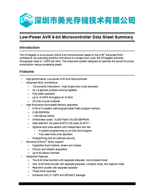
Low-Power AVR 8-bit Microcontroller Data Sheet Summary IntroductionThe ATmega8A is a low-power CMOS 8-bit microcontroller based on the AVR® enhanced RISC architecture. By executing powerful instructions in a single clock cycle, the ATmega8A achieves throughputs close to 1 MIPS per MHz. This empowers system designers to optimize the device for power consumption versus processing speed.Features•High-performance, Low-power AVR 8-bit Microcontroller•Advanced RISC Architecture–130 powerful instructions - most single-clock cycle execution–32 x 8 general purpose working registers–Fully static operation–Up to 16 MIPS throughput at 16 MHz–On-chip 2-cycle multiplier•High Endurance Nonvolatile Memory segments–8 KB of In-System Self-programmable Flash program memory–512B EEPROM– 1 KB internal SRAM–Write/erase cycles: 10,000 Flash/100,000 EEPROM–Data retention: 20 years at 85°C/100 years at 25°C(1)–Optional boot code section with independent lock bits•In-system programming by on-chip boot program•True read-while-write operation–Programming lock for software security•Microchip QTouch® library support–Capacitive touch buttons, sliders and wheels–QTouch and QMatrix acquisition–Up to 64 sense channels•Peripheral Features–Two 8-bit timer/counters with separate prescaler, one compare mode–One 16-bit timer/counter with separate prescaler, compare mode, and capture mode–Real-time counter with separate oscillator–Three PWM channels–8-channel ADC in TQFP and QFN/MLF package11.Packaging Information 11.1 32-pin 32A11.2 28-pin 28P311.3 32-pin 32M1-AErrata。
Atmega8型号细分区别

Atmega8型号细分区别ATMEGA8L- 8PU、ATMEGA8L-8PI、ATMEGA8L-8PC、ATMEGA8-16PU、ATMEGA8-16PI、ATMEGA8-16PC、ATMEGA8L-8AU、ATMEGA8L-8AI、ATMEGA8L-8AC、ATMEGA8-16AU、ATMEGA8-16AI、 ATMEGA8-16AC、ATMEGA8L-8MU、ATMEGA8L-8MI、ATMEGA8L-8MC、ATMEGA8-16MU、 ATMEGA8-16MI、ATMEGA8-16MC的区别如下:1.型号紧跟的字母,表示电压工作范围。
带“L”:2.7-5.5V;若缺省,不带“L”:4.5-5.5V。
例:ATmega8-16PU,不带“L”表示工作电压为4.5-5.5V。
2.后缀的数字部分,表示支持的最高系统时钟。
例:ATmega8-16PU,“16”表示可支持最高为16MHZ的系统时钟。
3.后缀第一(第二)个字母,表示封装。
“P”:DIP封装,“A”:TQFP封装,“M”:MLF封装。
例:ATmega8-16PU,“P”表示DIP封装。
;4.后缀最后一个字母,表示应用级别。
4.“C”:商业级,“I”:工业级(有铅)、“U”工业级(无铅)。
例:ATmega8-16PU,“U”表示无铅工业级。
ATmega8-16PI,“I”表示有铅工业级。
atmega328p晶体仪表的制作与程序
主题:atmega328p晶体仪表的制作与程序1. 简介atmega328p是一款由Atmel推出的低功耗、高性能的8位微控制器芯片,广泛应用于嵌入式系统和电子产品中。
通过合理的设计和程序编写,可以实现各种应用,比如晶体仪表。
下面将介绍如何制作atmega328p晶体仪表,并编写相应程序。
2. 材料准备- atmega328p芯片- 晶体振荡器- 电容- 电阻- LED数码管- 键盘- 电源及连线3. 硬件制作3.1 搭建电路连接3.2 确定晶体振荡器频率3.3 连接LED数码管3.4 键盘的连接3.5 完成整体电路连接4. 程序编写4.1 引用必要的库文件4.2 定义端口4.3 初始化程序4.4 程序编写流程及实现4.5 调试及优化5. 演示与调试5.1 上电演示5.2 程序功能演示5.3 调试过程及优化6. 总结atmega328p晶体仪表制作完成,并通过程序编写实现相应功能。
在制作过程中,需要严格按照电路连接图及引脚定义进行搭建,并注意电路的稳定性。
在程序编写时,需注重流程的合理性及代码的简洁性,以及功能的实现。
在演示与调试阶段,及时处理因硬件或软件方面的问题,并不断优化程序,以达到准确显示晶体信息的目的。
7. 参考资料- atmega328p数据手册- avr-gcc编程手册- 电路原理图及引脚定义通过上述步骤,我们可以很好的制作出atmega328p晶体仪表,并编写相应的程序,达到预期的功能。
希望以上内容对您有所帮助。
8. 扩展内容在制作atmega328p晶体仪表的过程中,除了搭建电路连接和编写程序外,还需要注意一些细节和技巧,以确保仪表的稳定性和准确性。
接下来,我们将深入探讨一些扩展内容,包括电路设计原则、程序优化技巧和应用场景的拓展。
8.1 电路设计原则在搭建电路连接过程中,电路设计是至关重要的一环。
为了确保atmega328p晶体仪表的稳定性和可靠性,需要遵循一些电路设计的原则:要合理设计电源部分。
ATMEGA8L-8AUR;ATMEGA8L-8MUR;中文规格书,Datasheet资料

Features•High-performance, Low-power Atmel®AVR® 8-bit Microcontroller •Advanced RISC Architecture–130 Powerful Instructions – Most Single-clock Cycle Execution –32 × 8 General Purpose Working Registers–Fully Static Operation–Up to 16MIPS Throughput at 16MHz–On-chip 2-cycle Multiplier•High Endurance Non-volatile Memory segments–8Kbytes of In-System Self-programmable Flash program memory–512Bytes EEPROM–1Kbyte Internal SRAM–Write/Erase Cycles: 10,000 Flash/100,000 EEPROM–Data retention: 20 years at 85°C/100 years at 25°C(1)–Optional Boot Code Section with Independent Lock BitsIn-System Programming by On-chip Boot ProgramTrue Read-While-Write Operation–Programming Lock for Software Security•Peripheral Features–Two 8-bit Timer/Counters with Separate Prescaler, one Compare Mode–One 16-bit Timer/Counter with Separate Prescaler, Compare Mode, and Capture Mode–Real Time Counter with Separate Oscillator–Three PWM Channels–8-channel ADC in TQFP and QFN/MLF packageEight Channels 10-bit Accuracy–6-channel ADC in PDIP packageSix Channels 10-bit Accuracy–Byte-oriented Two-wire Serial Interface–Programmable Serial USART–Master/Slave SPI Serial Interface–Programmable Watchdog Timer with Separate On-chip Oscillator–On-chip Analog Comparator•Special Microcontroller Features–Power-on Reset and Programmable Brown-out Detection–Internal Calibrated RC Oscillator–External and Internal Interrupt Sources–Five Sleep Modes: Idle, ADC Noise Reduction, Power-save, Power-down, andStandby•I/O and Packages–23 Programmable I/O Lines–28-lead PDIP, 32-lead TQFP, and 32-pad QFN/MLF•Operating Voltages–2.7V - 5.5V (ATmega8L)–4.5V - 5.5V (ATmega8)•Speed Grades–0 - 8MHz (ATmega8L)–0 - 16MHz (ATmega8)•Power Consumption at 4Mhz, 3V, 25°C–Active: 3.6mA–Idle Mode: 1.0mA–Power-down Mode: 0.5µA 8-bit with 8KBytesIn-System ProgrammableATmega8ATmega8L2ATmega8(L)PinConfigurationsATmega8(L) Overview The Atmel®AVR® ATmega8 is a low-power CMOS 8-bit microcontroller based on the AVR RISC architecture. By executing powerful instructions in a single clock cycle, the ATmega8 achievesthroughputs approaching 1MIPS per MHz, allowing the system designer to optimize power con-sumption versus processing speed.Block Diagram Figure 1. Block Diagram3 2486Z–AVR–02/1142486Z–AVR–02/11ATmega8(L)The Atmel ®AVR ® core combines a rich instruction set with 32 general purpose working registers.All the 32 registers are directly connected to the Arithmetic Logic Unit (ALU), allowing two inde-pendent registers to be accessed in one single instruction executed in one clock cycle. The resulting architecture is more code efficient while achieving throughputs up to ten times faster than conventional CISC microcontrollers.The ATmega8 provides the following features: 8 Kbytes of In-System Programmable Flash with Read-While-Write capabilities, 512 bytes of EEPROM, 1 Kbyte of SRAM, 23 general purpose I/O lines, 32 general purpose working registers, three flexible Timer/Counters with compare modes, internal and external interrupts, a serial programmable USART, a byte oriented Two-wire Serial Interface, a 6-channel ADC (eight channels in TQFP and QFN/MLF packages) with 10-bit accuracy, a programmable Watchdog Timer with Internal Oscillator, an SPI serial port,and five software selectable power saving modes. The Idle mode stops the CPU while allowing the SRAM, Timer/Counters, SPI port, and interrupt system to continue functioning. The Power-down mode saves the register contents but freezes the Oscillator, disabling all other chip func-tions until the next Interrupt or Hardware Reset. In Power-save mode, the asynchronous timer continues to run, allowing the user to maintain a timer base while the rest of the device is sleep-ing. The ADC Noise Reduction mode stops the CPU and all I/O modules except asynchronous timer and ADC, to minimize switching noise during ADC conversions. In Standby mode, the crystal/resonator Oscillator is running while the rest of the device is sleeping. This allows very fast start-up combined with low-power consumption.The device is manufactured using Atmel’s high density non-volatile memory technology. The Flash Program memory can be reprogrammed In-System through an SPI serial interface, by a conventional non-volatile memory programmer, or by an On-chip boot program running on the AVR core. The boot program can use any interface to download the application program in the Application Flash memory. Software in the Boot Flash Section will continue to run while the Application Flash Section is updated, providing true Read-While-Write operation. By combining an 8-bit RISC CPU with In-System Self-Programmable Flash on a monolithic chip, the Atmel ATmega8 is a powerful microcontroller that provides a highly-flexible and cost-effective solution to many embedded control applications.The ATmega8 is supported with a full suite of program and system development tools, including C compilers, macro assemblers, program debugger/simulators, In-Circuit Emulators, and evalu-ation kits.DisclaimerTypical values contained in this datasheet are based on simulations and characterization of other AVR microcontrollers manufactured on the same process technology. Minimum and Maxi-mum values will be available after the device is characterized.52486Z–AVR–02/11ATmega8(L)Pin DescriptionsVCC Digital supply voltage.GNDGround.Port B (PB7..PB0) XTAL1/XTAL2/TOSC1/TOSC2Port B is an 8-bit bi-directional I/O port with internal pull-up resistors (selected for each bit). The Port B output buffers have symmetrical drive characteristics with both high sink and source capability. As inputs, Port B pins that are externally pulled low will source current if the pull-up resistors are activated. The Port B pins are tri-stated when a reset condition becomes active,even if the clock is not running.Depending on the clock selection fuse settings, PB6 can be used as input to the inverting Oscil-lator amplifier and input to the internal clock operating circuit.Depending on the clock selection fuse settings, PB7 can be used as output from the inverting Oscillator amplifier.If the Internal Calibrated RC Oscillator is used as chip clock source, PB7..6 is used as TOSC2..1input for the Asynchronous Timer/Counter2 if the AS2 bit in ASSR is set.The various special features of Port B are elaborated in “Alternate Functions of Port B” on page 58 and “System Clock and Clock Options” on page 25.Port C (PC5..PC0)Port C is an 7-bit bi-directional I/O port with internal pull-up resistors (selected for each bit). The Port C output buffers have symmetrical drive characteristics with both high sink and source capability. As inputs, Port C pins that are externally pulled low will source current if the pull-up resistors are activated. The Port C pins are tri-stated when a reset condition becomes active,even if the clock is not running.PC6/RESETIf the RSTDISBL Fuse is programmed, PC6 is used as an I/O pin. Note that the electrical char-acteristics of PC6 differ from those of the other pins of Port C.If the RSTDISBL Fuse is unprogrammed, PC6 is used as a Reset input. A low level on this pin for longer than the minimum pulse length will generate a Reset, even if the clock is not running.The minimum pulse length is given in Table 15 on page 38. Shorter pulses are not guaranteed to generate a Reset.The various special features of Port C are elaborated on page 61.Port D (PD7..PD0)Port D is an 8-bit bi-directional I/O port with internal pull-up resistors (selected for each bit). The Port D output buffers have symmetrical drive characteristics with both high sink and source capability. As inputs, Port D pins that are externally pulled low will source current if the pull-up resistors are activated. The Port D pins are tri-stated when a reset condition becomes active,even if the clock is not running.Port D also serves the functions of various special features of the ATmega8 as listed on page 63.RESETReset input. A low level on this pin for longer than the minimum pulse length will generate a reset, even if the clock is not running. The minimum pulse length is given in Table 15 on page 38. Shorter pulses are not guaranteed to generate a reset.62486Z–AVR–02/11ATmega8(L)AV CCAV CC is the supply voltage pin for the A/D Converter, Port C (3..0), and ADC (7..6). It should be externally connected to V CC , even if the ADC is not used. If the ADC is used, it should be con-nected to V CC through a low-pass filter. Note that Port C (5..4) use digital supply voltage, V CC .AREFAREF is the analog reference pin for the A/D Converter.ADC7..6 (TQFP and QFN/MLF Package Only)In the TQFP and QFN/MLF package, ADC7..6 serve as analog inputs to the A/D converter.These pins are powered from the analog supply and serve as 10-bit ADC channels.ATmega8(L) Resources A comprehensive set of development tools, application notes and datasheets are available for download on /avr.Data Retention Reliability Qualification results show that the projected data retention failure rate is much less than 1 PPM over 20 years at 85°C or 100 years at 25°C.7 2486Z–AVR–02/1182486Z–AVR–02/11ATmega8(L)About Code ExamplesThis datasheet contains simple code examples that briefly show how to use various parts of the device. These code examples assume that the part specific header file is included before compi-lation. Be aware that not all C compiler vendors include bit definitions in the header files and interrupt handling in C is compiler dependent. Please confirm with the C compiler documentation for more details.92486Z–AVR–02/11ATmega8(L)Atmel AVR CPU CoreIntroductionThis section discusses the Atmel ®AVR ® core architecture in general. The main function of the CPU core is to ensure correct program execution. The CPU must therefore be able to access memories, perform calculations, control peripherals, and handle interrupts.Architectural OverviewFigure 2. Block Diagram of the AVR MCU ArchitectureIn order to maximize performance and parallelism, the AVR uses a Harvard architecture – with separate memories and buses for program and data. Instructions in the Program memory are executed with a single level pipelining. While one instruction is being executed, the next instruc-tion is pre-fetched from the Program memory. This concept enables instructions to be executed in every clock cycle. The Program memory is In-System Reprogrammable Flash memory.The fast-access Register File contains 32 × 8-bit general purpose working registers with a single clock cycle access time. This allows single-cycle Arithmetic Logic Unit (ALU) operation. In a typ-ical ALU operation, two operands are output from the Register File, the operation is executed,and the result is stored back in the Register File – in one clock cycle.Six of the 32 registers can be used as three 16-bit indirect address register pointers for Data Space addressing – enabling efficient address calculations. One of the these address pointers102486Z–AVR–02/11ATmega8(L)can also be used as an address pointer for look up tables in Flash Program memory. These added function registers are the 16-bit X-register, Y-register, and Z-register, described later in this section.The ALU supports arithmetic and logic operations between registers or between a constant and a register. Single register operations can also be executed in the ALU. After an arithmetic opera-tion, the Status Register is updated to reflect information about the result of the operation.The Program flow is provided by conditional and unconditional jump and call instructions, able to directly address the whole address space. Most AVR instructions have a single 16-bit word for-mat. Every Program memory address contains a 16-bit or 32-bit instruction.Program Flash memory space is divided in two sections, the Boot program section and the Application program section. Both sections have dedicated Lock Bits for write and read/write protection. The SPM instruction that writes into the Application Flash memory section must reside in the Boot program section.During interrupts and subroutine calls, the return address Program Counter (PC) is stored on the Stack. The Stack is effectively allocated in the general data SRAM, and consequently the Stack size is only limited by the total SRAM size and the usage of the SRAM. All user programs must initialize the SP in the reset routine (before subroutines or interrupts are executed). The Stack Pointer SP is read/write accessible in the I/O space. The data SRAM can easily be accessed through the five different addressing modes supported in the AVR architecture.The memory spaces in the AVR architecture are all linear and regular memory maps.A flexible interrupt module has its control registers in the I/O space with an additional global interrupt enable bit in the Status Register. All interrupts have a separate Interrupt Vector in the Interrupt Vector table. The interrupts have priority in accordance with their Interrupt Vector posi-tion. The lower the Interrupt Vector address, the higher the priority.The I/O memory space contains 64 addresses for CPU peripheral functions as Control Regis-ters, SPI, and other I/O functions. The I/O Memory can be accessed directly, or as the Data Space locations following those of the Register File, 0x20 - 0x5F.分销商库存信息:ATMELATMEGA8L-8AUR ATMEGA8L-8MUR。
ATmega328P中文翻译资料要点

(PCINT23/ AIN1)PD7
(PCINT0/ CLKO/ ICP1)PB0
PC5(ADC5/ SCL/ PCINT13)
PC4(ADC4/ SDA/ PCINT12)
PC3(ADC3/ PCINT11)
PC2(ADC2/ PCINT10)
PC1(ADC1/ PCINT9)
ADC7
GND
AREF
ADC6
AVCC
PB5(SCK/ PCINT5)
32
31
30
29
28
27
26
25
9
10
11
12
13
14
15
16
(PCINT21/ OC0B/ T 1)PD5
(PCINT22/ OC0A/ AIN0)PD6
(PCINT23/ AIN1)PD7
(PCINT0/ CLKO/ ICP1)PB0
32
31
30
29
28
27
26
25
9
10
11
12
13
14
15
16
32 MLF顶视图
(PCINT19/ OC2B/ INT1)PD3
(PCINT20/ XCK/ T0)PD4
GND
VCC
GND
VCC
(PCINT6/ XTAL1/ TOSC1)PB6
(PCINT7/ XTAL2/ TOSC2)PB7
PC1(ADC1/ PCINT9)
温度测量
- 6通道10位ADC PDIP封装
温度测量
-可编程的串行USART
-主/从SPI串行接口
Atmel 改变命名规则地芯片型号对照表

ATMLU对应ATMEL芯片:换代选型2011-04-25 23:57AT24C01BN-SH-B/T ATMEL ATMLU701 DIP AT24C01B-PU ATMEL ATMLU702 DIPAT24C02B-10PU-1.8 ATMEL ATMLU703 DIPAT24C02BN-SH-B/T ATMEL ATMLU704 DIP AT24C02B-PU ATMEL ATMLU705 DIPAT24C04-10PU-2.7 ATMEL ATMLU706 DIP AT24C04BN-SH-B ATMEL ATMLU707 DI PAT24C04N-10SU-2.7 ATMEL ATMLU708 DIPAT24C08A-10PU-2.7 ATMEL ATMLU709 DIPAT24C08A-10TU-2.7 ATMEL ATMLU710 DIPAT24C08AN-10SU-2.7 ATMEL ATMLU711 DIPAT24C128-10PU-2.7 ATMEL ATMLU712 DIPAT24C128N-10SU-2.7-SL383 ATMEL ATMLU713 DIPAT24C16A-10PU-2.7 ATMEL ATMLU714 DIPAT24C16A-10TI-1.8 ATMEL ATMLU715 DIP AT24C16AN-10SU-2.7 ATMEL ATMLU716 DIPAT24C16BN-SH-B ATMEL ATMLU717 DIP AT24C256B-10PU-1.8 ATMEL ATMLU718 DIPAT24C256BN-10SU-1.8 ATMEL ATMLU719DIPAT24C256BN-SH-T ATMEL ATMLU720 DIPAT24C256B-PU ATMELATMLU721 DIPAT24C256N-10SI18 ATMEL ATMLU722 DIPAT24C32A-10PU-2.7 ATMEL ATMLU723 DIPAT24C32AN-10SU-2.7 ATMEL ATMLU724 DIPAT24C32CN-SH-T ATMEL ATMLU72 5 DIPAT24C512-10PU-2.7 ATMEL ATMLU726 DIPAT24C512BN-SH25-B ATMEL ATMLU727 DIPAT24C512BN-SH-B ATMEL ATMLU728 DIP29 DIPAT24C512N-10SU-2.7 ATMEL ATMLU730 DIPAT24C64A-10PU-2.7 ATMEL ATMLU731 DIPAT24C64AN-10SU-2.7 ATMEL ATMLU732 DIPAT24C64CN-SH-B ATMEL ATMLU7 33 DIPAT24C64CN-SH-T ATMEL ATMLU73 4 DIPAT25128A-10PU-2.7 ATMEL ATMLU735 DIPAT25256AN-10SU-2.7 ATMEL ATMLU736 DIPAT25DF041A-SH-B ATMEL ATMLU737 DIPAT25F1024AN-10SU-2.7-SL383 ATMELATMLU738 DIPAT25F512AN-10SU-2.7-SL383 ATMELATMLU739 DIPAT26DF081A-SSU-SL965 ATMELATMLU740 DIPAT26DF081A-SU-SL965 ATME L ATMLU741 DIPAT26DF161-SUATMEL ATMLU742 DIPAT26DF321-SU ATMELATMLU743 DIPAT27BV256-70JU ATMEL ATMLU744 DIPAT27C010-70PU ATMEL ATMLU74 5 DIPAT27C040-70PU ATMEL ATMLU746DIPAT27C256R-70JU ATMEL ATMLU747DIPAT27C256R-70PU ATMEL ATMLU748DIPAT27C512R-70JU ATMEL ATMLU749 DIPAT28BV256-20TU ATMEL ATMLU750 DIPDIPAT28C64B-15JU ATMEL ATMLU752 DIPAT28C64B-15PU ATMEL ATMLU801 DIPAT28C64B-15SU ATMEL ATMLU802 DIPAT29C010A-70JU ATMEL ATMLU803 DIPAT29C020-90JU ATMEL ATMLU80 4 DIPAT29C020-90TU ATMEL ATMLU805 DIPAT29C040A-90JU ATMEL ATMLU806 DIPAT29C040A-90TU ATMEL ATMLU807DIPAT29LV020-10TU ATMEL ATMLU808 DIPAT29LV040A-15JU ATMEL ATMLU809 DIPAT29LV512-12JU ATMEL ATMLU810 DIPAT45DB021B-SU ATMEL ATMLU811 DIPAT45DB041D-SU ATMEL ATMLU812 DIPAT45DB081D-SU ATMEL ATMLU813DIPAT45DB161D-SU ATMEL ATMLU814 DIPAT45DB161D-TU ATMEL ATMLU815DIPAT45DB321D-SU ATMEL ATMLU816 DIPAT45DB321D-TU ATMEL ATMLU817 DIPAT45DB642D-TU ATMEL ATMLU818 DIPAT47BV163A-70TU ATMEL ATMLU819 DIPAT49BV040B-JU ATMEL ATMLU820 DIPAT49BV322DT-70TU ATMEL ATMLU821 DIPAT49BV512-90TU ATMEL ATMLU822 DIPAT73C213 ATMEL ATMLU823 DIPAT76C112 ATMEL ATMLU824 DIPAT76C120H-MU1-JZ208 ATMEL ATMLU825 DIPAT80251G2D-SLSUM ATMEL ATMLU826 DIP AT80C32X2-3CSUM ATMEL ATMLU827 DIPAT80C32X2-RLTUM ATMEL ATMLU828 DIPAT80C32X2-SLSUM ATMEL ATMLU829 DIPAT83C24-TISIL ATMEL ATMLU830 DIPAT88SC0104C-SU ATMEL ATMLU831 DIPAT88SC153-10SU ATMEL ATMLU832 DIPAT89C2051-12PU ATMEL ATMLU833 DIPAT89C2051-12SU ATMEL ATMLU834 DIPAT89C2051-24PU ATMEL ATMLU835 DIPAT89C2051-24SU ATMEL ATMLU836 DIPAT89C4051-24PU ATMEL ATMLU837 DIPAT89C4051-24SU ATMEL ATMLU838 DIPAT89C5131A-S3SUM ATMEL ATMLU839 DIP AT89C51AC2-RLTUM ATMEL ATMLU840 DIP AT89C51CC01CA-RLTUM ATMEL ATMLU841 DIP AT89C51CC01CA-SLSUM ATMEL ATMLU842 DIP AT89C51CC01UA-RLTUM ATMEL ATMLU843 DIP AT89C51CC01UA-SLSUM ATMEL ATMLU844 DIP AT89C51ED2-RDTUM ATMEL ATMLU845 DIP AT89C51ED2-RLTUM ATMEL ATMLU846 DIP AT89C51ED2-SLSUM ATMEL ATMLU847 DIP AT89C51ED2-SMSUM ATMEL ATMLU848 DIP AT89C51RB2-3CSUM ATMEL ATMLU849 DIP AT89C51RB2-RLTUM ATMEL ATMLU850 DIP AT89C51RB2-SLSUM ATMEL ATMLU851 DIP AT89C51RC2-3CSUM ATMEL ATMLU852 DIP AT89C51RC-24JU ATMEL ATMLU901 DIPAT89C51RC-24PU ATMEL ATMLU902 DIPAT89C51RC2-RLTUM ATMEL ATMLU903 DIP AT89C51RC2-SLSUM ATMEL ATMLU904 DIP AT89C51RD2-RLTUM ATMEL ATMLU905 DIP AT89C51RD2-SLRUM ATMEL ATMLU906 DIP AT89C51RD2-SLSUM ATMEL ATMLU907 DIP AT89C51-24PC ATMEL ATMLU908 DIPAT89C51-24PI ATMEL ATMLU909 DIPAT89C52-24JI ATMEL ATMLU910 DIPAT89C52-24PI ATMEL ATMLH701 SOPAT89C55WD-24AU ATMEL ATMLH702 SOPAT89C55WD-24JU ATMEL ATMLH703 SOPAT89C55WD-24PU ATMEL ATMLH704 SOPAT89LS52-16JU ATMEL ATMLH705 SOPAT89LS52-16PU ATMEL ATMLH706 SOPAT89LV51-12AI ATMEL ATMLH707 SOPAT89S51-24PU ATMEL ATMLH709 SOPAT89S52-24AU ATMEL ATMLH710 SOPAT89S52-24JU ATMEL ATMLH711 SOPAT89S52-24PU ATMEL ATMLH712 SOPAT89S54-3CSIM ATMEL ATMLH713 SOPAT89S54-SLSIM ATMEL ATMLH714 SOPAT89S58-SLSIM ATMEL ATMLH715 SOPAT89S8253-24AU ATMEL ATMLH716 SOPAT89S8253-24JU ATMEL ATMLH717 SOPAT89S8253-24PU ATMEL ATMLH718 SOPAT90CAN128-16AU ATMEL ATMLH719 SOPAT90CAN32-16AU ATMEL ATMLH720 SOPAT91M40800-33AU ATMEL ATMLH721 SOPAT91M55800A-33AU ATMEL ATMLH722 SOPAT91RM9200-CJ-002 ATMEL ATMLH723 SOPAT91RM9200-QU-002 ATMEL ATMLH724 SOPAT91SAM7S256-AU-001 ATMEL ATMLH725 SOPAT91SAM7S321-AU ATMEL ATMLH726 SOPAT91SAM7S32-AU-001 ATMEL ATMLH727 SOPAT91SAM7S64-AU-001 ATMEL ATMLH728 SOPAT91SAM7SE32-AU ATMEL ATMLH729 SOPAT91SAM7X256-AU ATMEL ATMLH730 SOPAT91SAM9260-CJ ATMEL ATMLH731 SOPAT91SAM9260-EK ATMEL ATMLH732 SOPAT91SAM9261-EK ATMEL ATMLH733 SOPAT91SAM9261S-CU ATMEL ATMLH734 SOPAT91SAM9263-CU ATMEL ATMLH735 SOPAT91SAM7X-EK ATMEL ATMLH736 SOPAT91SAM-ICE ATMEL ATMLH737 SOPAT93C46-10PU-2.7 ATMEL ATMLH738 SOPAT93C46-10SU-2.7 ATMEL ATMLH739 SOPAT93C46DN-SH-B ATMEL ATMLH740 SOPAT93C46D-TH-T ATMEL ATMLH741 SOPAT93C56A-10PU-2.7 ATMEL ATMLH742 SOPAT93C56A-10SU-2.7 ATMEL ATMLH743 SOPAT93C66A-10PU27 ATMEL ATMLH744 SOPAT93C66A-10SU-2.7 ATMEL ATMLH745 SOPAT93C66A-10SU-2.7-SL383 ATMEL ATMLH746 SOP ATAVRDRAGON ATMEL ATMLH747 SOPATAVRISP2 ATMEL ATMLH748 SOPATF1502AS-15JC44 ATMEL ATMLH749 SOPATF1508AS-15AC100 ATMEL ATMLH750 SOPATF1508AS-15JC84 ATMEL ATMLH751 SOPATF16V8B-15PC ATMEL ATMLH801 SOP ATF16V8B-15PU ATMEL ATMLH802 SOP ATF16V8BQL-15JC ATMEL ATMLH803 SOP ATF20V8B-15JC ATMEL ATMLH804 SOP ATJTAGICE2 ATMEL ATMLH805 SOP ATMEGA1280V-8AU ATMEL ATMLH806 SOP ATMEGA128-16AU ATMEL ATMLH807 SOP ATMEGA128L-8AU ATMEL ATMLH808 SOP ATMEGA16-16AU ATMEL ATMLH809 SOP ATMEGA16-16PU ATMEL ATMLH810 SOP ATMEGA162-16PU ATMEL ATMLH811 SOP ATMEGA162V-8AU ATMEL ATMLH812 SOP ATMEGA168-20AU ATMEL ATMLH813 SOP ATMEGA168-20MU ATMEL ATMLH814 SOP ATMEGA168-20PU ATMEL ATMLH815 SOP ATMEGA168V-10AU ATMEL ATMLH816 SOP ATMEGA169P-16AU ATMEL ATMLH817 SOP ATMEGA169PV-8AU ATMEL ATMLH818 SOP ATMEGA169V-8AU ATMEL ATMLH819 SOP ATMEGA16L-8AU ATMEL ATMLH820 SOP ATMEGA16L-8PU ATMEL ATMLH821 SOP ATMEGA32-16AU ATMEL ATMLH822 SOP ATMEGA32-16PU ATMEL ATMLH823 SOP ATMEGA325V-8MU ATMEL ATMLH824 SOP ATMEGA32L-8AU ATMEL ATMLH825 SOP ATMEGA32L-8PU ATMEL ATMLH826 SOP ATMEGA48-20AU ATMEL ATMLH827 SOP ATMEGA48V-10AU ATMEL ATMLH828 SOP ATMEGA48V-10PU ATMEL ATMLH829 SOP ATMEGA48V-10MU ATMEL ATMLH830 SOP ATMEGA640V-8AU ATMEL ATMLH831 SOP ATMEGA64-16AU ATMEL ATMLH832 SOP ATMEGA64L-8AU ATMEL ATMLH833 SOP ATMEGA8-16AU ATMEL ATMLH834 SOP ATMEGA8-16PU ATMEL ATMLH835 SOP ATMEGA8515-16AU ATMEL ATMLH836 SOP ATMEGA8515-16JU ATMEL ATMLH837 SOP ATMEGA8515-16PU ATMEL ATMLH838 SOP ATMEGA8515L-8JU ATMEL ATMLH839 SOP ATMEGA8535-16JI ATMEL ATMLH840 SOP ATMEGA8535-16JU ATMEL ATMLH841 SOP ATMEGA8535-16PU ATMEL ATMLH842 SOP ATMEGA8535L-8AU ATMEL ATMLH843 SOPATMEGA8535L-8PU ATMEL ATMLH845 SOP ATMEGA88-20AU ATMEL ATMLH846 SOPATMEGA88-20MU ATMEL ATMLH847 SOPATMEGA88-20PU ATMEL ATMLH848 SOPATMEGA88V-10AU ATMEL ATMLH849 SOPATMEGA88V-10MU ATMEL ATMLH850 SOPATMEGA88V-10PU ATMEL ATMLH851 SOPATMEGA8L-8AU ATMEL ATMLH852 SOPATMEGA8L-8PU ATMEL ATMLH901 SOPATTINY11L-2SU ATMEL ATMLH902 SOPATTINY13-20SU ATMEL ATMLH903 SOPATTINY13V-10PU ATMEL ATMLH904 SOPATTINY13V-10SSU ATMEL ATMLH905 SOPATTINY13V-10SU ATMEL ATMLH906 SOPATTINY15L-1PU ATMEL ATMLH907 SOPATTINY2313-20PU ATMEL ATMLH908 SOPATTINY2313-20SU ATMEL ATMLH909 SOPATTINY2313V-10PU ATMEL ATMLH910 SOPAT24C01BN-SH-B/T ATMEL ATMLU701 DIPAT24C01B-PI ATMEL ATMLU702 DIPAT24C02B-10PI-1.8 ATMEL ATMLU703 DIPAT24C02BN-SH-B/T ATMEL ATMLU704 DIPAT24C02B-PI ATMEL ATMLU705 DIPAT24C04-10PI-2.7 ATMEL ATMLU706 DIPAT24C04BN-SH-B ATMEL ATMLU707 DIPAT24C04N-10SI-2.7 ATMEL ATMLU708 DIPAT24C08A-10PI-2.7 ATMEL ATMLU709 DIPAT24C08A-10TI-2.7 ATMEL ATMLU710 DIPAT24C08AN-10SI-2.7 ATMEL ATMLU711 DIPAT24C128-10PI-2.7 ATMEL ATMLU712 DIPAT24C128N-10SI-2.7-SL383 ATMEL ATMLU713 DIP AT24C16A-10PI-2.7 ATMEL ATMLU714 DIPAT24C16A-10TI-1.8 ATMEL ATMLU715 DIPAT24C16AN-10SI-2.7 ATMEL ATMLU716 DIPAT24C16BN-SH-B ATMEL ATMLU717 DIPAT24C256B-10PI-1.8 ATMEL ATMLU718 DIPAT24C256BN-10SI-1.8 ATMEL ATMLU719 DIPAT24C256BN-SH-T ATMEL ATMLU720 DIPAT24C256B-PI ATMEL ATMLU721 DIPAT24C256N-10SI18 ATMEL ATMLU722 DIPAT24C32A-10PI-2.7 ATMEL ATMLU723 DIPAT24C32AN-10SI-2.7 ATMEL ATMLU724 DIPAT24C32CN-SH-T ATMEL ATMLU725 DIPAT24C512-10PI-2.7 ATMEL ATMLU726 DIPAT24C512BN-SH25-B ATMEL ATMLU727 DIPAT24C512BN-SH-B ATMEL ATMLU728 DIPAT24C512B-PI25 ATMEL ATMLU729 DIPAT24C512N-10SI-2.7 ATMEL ATMLU730 DIPAT24C64A-10PI-2.7 ATMEL ATMLU731 DIPAT24C64AN-10SI-2.7 ATMEL ATMLU732 DIPAT24C64CN-SH-B ATMEL ATMLU733 DIPAT24C64CN-SH-T ATMEL ATMLU734 DIPAT25128A-10PI-2.7 ATMEL ATMLU735 DIPAT25256AN-10SI-2.7 ATMEL ATMLU736 DIPAT25DF041A-SH-B ATMEL ATMLU737 DIPAT25F1024AN-10SI-2.7-SL383 ATMEL ATMLU738 DIP AT25F512AN-10SI-2.7-SL383 ATMEL ATMLU739 DIP AT26DF081A-SSI-SL965 ATMEL ATMLU740 DIPAT26DF081A-SI-SL965 ATMEL ATMLU741 DIPAT26DF161-SI ATMEL ATMLU742 DIPAT26DF321-SI ATMEL ATMLU743 DIPAT27BV256-70JI ATMEL ATMLU744 DIPAT27C010-70PI ATMEL ATMLU745 DIPAT27C040-70PI ATMEL ATMLU746 DIPAT27C256R-70JI ATMEL ATMLU747 DIPAT27C256R-70PI ATMEL ATMLU748 DIPAT27C512R-70JI ATMEL ATMLU749 DIPAT28BV256-20TI ATMEL ATMLU750 DIPAT28C256-15PI ATMEL ATMLU751 DIPAT28C64B-15JI ATMEL ATMLU752 DIPAT28C64B-15PI ATMEL ATMLU801 DIPAT28C64B-15SI ATMEL ATMLU802 DIPAT29C010A-70JI ATMEL ATMLU803 DIPAT29C020-90JI ATMEL ATMLU804 DIPAT29C020-90TI ATMEL ATMLU805 DIPAT29C040A-90JI ATMEL ATMLU806 DIPAT29C040A-90TI ATMEL ATMLU807 DIPAT29LV020-10TI ATMEL ATMLU808 DIPAT29LV040A-15JI ATMEL ATMLU809 DIPAT29LV512-12JI ATMEL ATMLU810 DIPAT45DB021B-SI ATMEL ATMLU811 DIPAT45DB041D-SI ATMEL ATMLU812 DIPAT45DB081D-SI ATMEL ATMLU813 DIPAT45DB161D-SI ATMEL ATMLU814 DIPAT45DB161D-TI ATMEL ATMLU815 DIPAT45DB321D-SI ATMEL ATMLU816 DIPAT45DB321D-TI ATMEL ATMLU817 DIPAT47BV163A-70TI ATMEL ATMLU819 DIPAT49BV040B-JI ATMEL ATMLU820 DIPAT49BV322DT-70TI ATMEL ATMLU821 DIP AT49BV512-90TI ATMEL ATMLU822 DIPAT73C213 ATMEL ATMLU823 DIPAT76C112 ATMEL ATMLU824 DIPAT76C120H-MI1-JZ208 ATMEL ATMLU825 DIP AT80251G2D-SLSIM ATMEL ATMLU826 DIP AT80C32X2-3CSIM ATMEL ATMLU827 DIPAT80C32X2-RLTIM ATMEL ATMLU828 DIPAT80C32X2-SLSIM ATMEL ATMLU829 DIPAT83C24-TISIL ATMEL ATMLU830 DIPAT88SC0104C-SI ATMEL ATMLU831 DIPAT88SC153-10SI ATMEL ATMLU832 DIPAT89C2051-12PI ATMEL ATMLU833 DIPAT89C2051-12SI ATMEL ATMLU834 DIPAT89C2051-24PI ATMEL ATMLU835 DIPAT89C2051-24SI ATMEL ATMLU836 DIPAT89C4051-24PI ATMEL ATMLU837 DIPAT89C4051-24SI ATMEL ATMLU838 DIPAT89C5131A-S3SIM ATMEL ATMLU839 DIP AT89C51AC2-RLTIM ATMEL ATMLU840 DIP AT89C51CC01CA-RLTIM ATMEL ATMLU841 DIP AT89C51CC01CA-SLSIM ATMEL ATMLU842 DIP AT89C51CC01IA-RLTIM ATMEL ATMLU843 DIP AT89C51CC01IA-SLSIM ATMEL ATMLU844 DIP AT89C51ED2-RDTIM ATMEL ATMLU845 DIP AT89C51ED2-RLTIM ATMEL ATMLU846 DIP AT89C51ED2-SLSIM ATMEL ATMLU847 DIP AT89C51ED2-SMSIM ATMEL ATMLU848 DIP AT89C51RB2-3CSIM ATMEL ATMLU849 DIP AT89C51RB2-RLTIM ATMEL ATMLU850 DIP AT89C51RB2-SLSIM ATMEL ATMLU851 DIP AT89C51RC2-3CSIM ATMEL ATMLU852 DIP AT89C51RC-24JI ATMEL ATMLU901 DIPAT89C51RC-24PI ATMEL ATMLU902 DIPAT89C51RC2-RLTIM ATMEL ATMLU903 DIP AT89C51RC2-SLSIM ATMEL ATMLU904 DIP AT89C51RD2-RLTIM ATMEL ATMLU905 DIP AT89C51RD2-SLRIM ATMEL ATMLU906 DIP AT89C51RD2-SLSIM ATMEL ATMLU907 DIP AT89C51-24PC ATMEL ATMLU908 DIPAT89C51-24PI ATMEL ATMLU909 DIPAT89C52-24PI ATMEL ATMLH701 SOPAT89C55WD-24AI ATMEL ATMLH702 SOPAT89C55WD-24JI ATMEL ATMLH703 SOPAT89C55WD-24PI ATMEL ATMLH704 SOPAT89LS52-16JI ATMEL ATMLH705 SOPAT89LS52-16PI ATMEL ATMLH706 SOPAT89LV51-12AI ATMEL ATMLH707 SOPAT89S51-24AI ATMEL ATMLH708 SOPAT89S51-24PI ATMEL ATMLH709 SOPAT89S52-24AI ATMEL ATMLH710 SOPAT89S52-24JI ATMEL ATMLH711 SOPAT89S52-24PI ATMEL ATMLH712 SOPAT89S54-3CSIM ATMEL ATMLH713 SOPAT89S54-SLSIM ATMEL ATMLH714 SOPAT89S58-SLSIM ATMEL ATMLH715 SOPAT89S8253-24AI ATMEL ATMLH716 SOPAT89S8253-24JI ATMEL ATMLH717 SOPAT89S8253-24PI ATMEL ATMLH718 SOPAT90CAN128-16AI ATMEL ATMLH719 SOPAT90CAN32-16AI ATMEL ATMLH720 SOPAT91M40800-33AI ATMEL ATMLH721 SOPAT91M55800A-33AI ATMEL ATMLH722 SOP AT91RM9200-CJ-002 ATMEL ATMLH723 SOP AT91RM9200-QI-002 ATMEL ATMLH724 SOP AT91SAM7S256-AI-001 ATMEL ATMLH725 SOP AT91SAM7S321-AI ATMEL ATMLH726 SOPAT91SAM7S32-AI-001 ATMEL ATMLH727 SOP AT91SAM7S64-AI-001 ATMEL ATMLH728 SOP AT91SAM7SE32-AI ATMEL ATMLH729 SOPAT91SAM7X256-AI ATMEL ATMLH730 SOPAT91SAM9260-CJ ATMEL ATMLH731 SOPAT91SAM9260-EK ATMEL ATMLH732 SOPAT91SAM9261-EK ATMEL ATMLH733 SOPAT91SAM9261S-CI ATMEL ATMLH734 SOPAT91SAM9263-CI ATMEL ATMLH735 SOPAT91SAM7X-EK ATMEL ATMLH736 SOPAT91SAM-ICE ATMEL ATMLH737 SOPAT93C46-10PI-2.7 ATMEL ATMLH738 SOP AT93C46-10SI-2.7 ATMEL ATMLH739 SOP AT93C46DN-SH-B ATMEL ATMLH740 SOPAT93C46D-TH-T ATMEL ATMLH741 SOPAT93C56A-10PI-2.7 ATMEL ATMLH742 SOP AT93C56A-10SI-2.7 ATMEL ATMLH743 SOPAT93C66A-10SI-2.7 ATMEL ATMLH745 SOPAT93C66A-10SI-2.7-SL383 ATMEL ATMLH746 SOP ATAVRDRAGON ATMEL ATMLH747 SOPATAVRISP2 ATMEL ATMLH748 SOPATF1502AS-15JC44 ATMEL ATMLH749 SOPATF1508AS-15AC100 ATMEL ATMLH750 SOPATF1508AS-15JC84 ATMEL ATMLH751 SOPATF16V8B-15JI ATMEL ATMLH752 SOPATF16V8B-15PC ATMEL ATMLH801 SOPATF16V8B-15PI ATMEL ATMLH802 SOPATF16V8BQL-15JC ATMEL ATMLH803 SOPATF20V8B-15JC ATMEL ATMLH804 SOPAT JTAGICE MKII ATMEL ATMLH805 SOP ATMEGA1280V-8AI ATMEL ATMLH806 SOP ATMEGA128-16AI ATMEL ATMLH807 SOP ATMEGA128L-8AI ATMEL ATMLH808 SOP ATMEGA16-16AI ATMEL ATMLH809 SOPATMEGA16-16PI ATMEL ATMLH810 SOPATMEGA162-16PI ATMEL ATMLH811 SOP ATMEGA162V-8AI ATMEL ATMLH812 SOP ATMEGA168-20AI ATMEL ATMLH813 SOP ATMEGA168-20MI ATMEL ATMLH814 SOP ATMEGA168-20PI ATMEL ATMLH815 SOP ATMEGA168V-10AI ATMEL ATMLH816 SOP ATMEGA169P-16AI ATMEL ATMLH817 SOP ATMEGA169PV-8AI ATMEL ATMLH818 SOP ATMEGA169V-8AI ATMEL ATMLH819 SOP ATMEGA16L-8AI ATMEL ATMLH820 SOPATMEGA16L-8PI ATMEL ATMLH821 SOPATMEGA32-16AI ATMEL ATMLH822 SOPATMEGA32-16PI ATMEL ATMLH823 SOPATMEGA325V-8MI ATMEL ATMLH824 SOP ATMEGA32L-8AI ATMEL ATMLH825 SOPATMEGA32L-8PI ATMEL ATMLH826 SOPATMEGA48-20AI ATMEL ATMLH827 SOPATMEGA48V-10AI ATMEL ATMLH828 SOP ATMEGA48V-10PI ATMEL ATMLH829 SOP ATMEGA48V-10MI ATMEL ATMLH830 SOP ATMEGA640V-8AI ATMEL ATMLH831 SOP ATMEGA64-16AI ATMEL ATMLH832 SOPATMEGA64L-8AI ATMEL ATMLH833 SOPATMEGA8-16AI ATMEL ATMLH834 SOPATMEGA8-16PI ATMEL ATMLH835 SOPATMEGA8515-16JI ATMEL ATMLH837 SOP ATMEGA8515-16PI ATMEL ATMLH838 SOP ATMEGA8515L-8JI ATMEL ATMLH839 SOP ATMEGA8535-16JI ATMEL ATMLH840 SOP ATMEGA8535-16JI ATMEL ATMLH841 SOP ATMEGA8535-16PI ATMEL ATMLH842 SOP ATMEGA8535L-8AI ATMEL ATMLH843 SOP ATMEGA8535L-8JI ATMEL ATMLH844 SOP ATMEGA8535L-8PI ATMEL ATMLH845 SOP ATMEGA88-20AI ATMEL ATMLH846 SOP ATMEGA88-20MI ATMEL ATMLH847 SOP ATMEGA88-20PI ATMEL ATMLH848 SOP ATMEGA88V-10AI ATMEL ATMLH849 SOP ATMEGA88V-10MI ATMEL ATMLH850 SOP ATMEGA88V-10PI ATMEL ATMLH851 SOP ATMEGA8L-8AI ATMEL ATMLH852 SOP ATMEGA8L-8PI ATMEL ATMLH901 SOP ATTINY11L-2SI ATMEL ATMLH902 SOP ATTINY13-20SI ATMEL ATMLH903 SOP ATTINY13V-10PI ATMEL ATMLH904 SOP ATTINY13V-10SSI ATMEL ATMLH905 SOP ATTINY13V-10SI ATMEL ATMLH906 SOP ATTINY15L-1PI ATMEL ATMLH907 SOP ATTINY2313-20PI ATMEL ATMLH908 SOP ATTINY2313-20SI ATMEL ATMLH909 SOP ATTINY2313V-10PI ATMEL ATMLH910 SOP AT17LV010-10PI 1000 ATMEL0007AT17LV256-10JI 1000 ATMEL0008AT17LV256-10PC 1000 ATMEL0009AT17LV256-10PI 1000 ATMEL0010AT17LV512-10PC 1000 ATMEL0011AT17LV512-10PC 1000 ATMEL0012AT17LV512A-10PI 1000 ATMEL0013AT17LV65-10PI 1000 ATMEL0014AT22V10-15DC 1000 ATMEL0015AT22V10-15JC 1000 ATMEL0016AT22V10-15KC 1000 ATMEL0017AT22V10-20DC 1000 ATMEL0018AT22V10-20JC 1000 ATMEL0019AT22V10-25DC 1000 ATMEL0020AT22V10-25JC 1000 ATMEL0021AT22V10-25JI 1000 ATMEL0022AT22V10-25KC 1000 ATMEL0023AT22V10-35DC 1000 ATMEL0024AT22V10-35JC 1000 ATMEL0025AT22V10-35KC 1000 ATMEL0026AT22V10-35PC 1000 ATMEL0027AT22V10L-20PC 1000 ATMEL0028AT22V10L-25DC 1000 ATMEL0029AT22V10L-25JC 1000 ATMEL0030AT22V10L-25JI 1000 ATMEL0031AT22V10L-35DC 1000 ATMEL0032AT24C01-10PC 1000 ATMEL0033AT24C01-10PC2.5 1000 ATMEL0034 AT24C01-10PI 1000 ATMEL0035AT24C01-10PI2.5 1000 ATMEL0036 AT24C01-10SC 1000 ATMEL0037AT24C01A-10PC 8000 ATMEL0038AT24C01A-10SC 8000 ATMEL0039AT24C01A-10SI2.7 8000 ATMEL0040 AT24C01A-10SU-1.8V 8000 ATMEL0601 AT24C01A-10TI2.7 8000 ATMEL0041 AT24C01BN-SH-B 8000 ATMEL0042AT24C01BN-SH-T 8000 ATMEL0043AT24C01B-PU 8000 ATMEL0602AT24C01B-TH-B 8000 ATMEL0044AT24C01B-TH-T 8000 ATMEL0045AT24C01BTSU-T 8000 ATMEL0603AT24C01BU3-UU-T 8000 ATMEL0604 AT24C01B-W-11 8000 ATMEL0046AT24C01BY6-YH-T 8000 ATMEL0047 AT24C01N-10SC2.7 8000 ATMEL0048 AT24C02-10PC 8000 ATMEL0049AT24C02-10PC1.8 8000 ATMEL0050 AT24C02-10PI2.7 8000 ATMEL0051 AT24C02-10TI2.7 8000 ATMEL0052 AT24C02AN-10SU2.7 8000 ATMEL0605 AT24C02N-10SC1.8 8000 ATMEL0101 AT24C02N-10SI1.8 8000 ATMEL0102 AT24C04-10PI2.7 8000 ATMEL0103 AT24C04-10PU-2.7V 8000 ATMEL0606 AT24C04-10TI-2.7 8000 ATMEL0104 AT24C04-10TU-2.7 8000 ATMEL0607 AT24C04A-10TI-2.7 8000 ATMEL0105 AT24C04N-10SI1.8 8000 ATMEL0106 AT24C08-10PI2.7 8000 ATMEL0107 AT24C08A-10TI2.7 8000 ATMEL0108AT24C08AN-10SU2.7 8000 ATMEL0608 AT24C1024-10PI2.7 8000 ATMEL0110 AT24C1024W-10SI2.7 8000 ATMEL0111 AT24C11-10PI-1.8 8000 ATMEL0112 AT24C11-10PI-2.7 8000 ATMEL0113 AT24C11-10PI-2.7 8000 ATMEL0114 AT24C11-10PU-1.8 8000 ATMEL0609 AT24C11-10PU-2.7 8000 ATMEL0610 AT24C11-10TI-1.8 8000 ATMEL0115 AT24C11-10TI-2.7 8000 ATMEL0116 AT24C11-10TQ-2.7 8000 ATMEL0117 AT24C11-10TSU-1.8 8000 ATMEL0611 AT24C11-10TU-1.8 8000 ATMEL0612 AT24C11-10TU-2.7 8000 ATMEL0613 AT24C11N-10SI-1.8 8000 ATMEL0118 AT24C11N-10SI-2.7 8000 ATMEL0119 AT24C11N-10SQ-2.7 8000 ATMEL0120 AT24C11N-10SU-1.8 8000 ATMEL0614 AT24C11N-10SU-2.7 8000 ATMEL0615 AT24C11-W1.8-11 8000 ATMEL0121 AT24C11-W2.7-11 8000 ATMEL0122 AT24C128-10PI2.7 8000 ATMEL0123 AT24C128-10TU-1.8 8000 ATMEL0616 AT24C128-10TU-2.7 8000 ATMEL0617 AT24C128N-10SI1.8 8000 ATMEL0124 AT24C128N-10SI2.7 8000 ATMEL0125 AT24C16-10PI 8000 ATMEL0126AT24C16-10TC1.8 8000 ATMEL0127 AT24C164-10PC 8000 ATMEL0128AT24C164-10PC2.7 8000 ATMEL0129 AT24C164-10PI 8000 ATMEL0130AT24C164-10SC 8000 ATMEL0131AT24C164-10SI1.8 8000 ATMEL0132 AT24C164-10SI2.7 8000 ATMEL0133 AT24C164-10SI-2.7 8000 ATMEL0134 AT24C16A-10PI2.7 8000 ATMEL0135 AT24C16A-10TI1.8 8000 ATMEL0136 AT24C16AN-10SI1.8 8000 ATMEL0137 AT24C16AN-10SI2.7 8000 ATMEL0138 AT24C16N-SC 8000 ATMEL0139AT24C16N-SI2.7 8000 ATMEL0140AT24C21-10PC2.5 8000 ATMEL0141 AT24C21-10PC-2.5 8000 ATMEL0142AT24C21-10SI2.5 8000 ATMEL0144 AT24C21-SC2.5 8000 ATMEL0145AT24C256-10CI-2.7 8000 ATMEL0146 AT24C256-10PC 8000 ATMEL0147AT24C256-10PI2.7 8000 ATMEL0148 AT24C256-10TI2.7 8000 ATMEL0149 AT24C256N-10SI1.8 8000 ATMEL0150 AT24C256N-10SI2.7 8000 ATMEL0151 AT24C256T1-10TI2.7 8000 ATMEL0152 AT24C257N-10SC-2.7 8000 ATMEL0201 AT24C32-10PC 8000 ATMEL0202AT24C32-10PI2.7 8000 ATMEL0203 AT24C32A-10PI2.7 8000 ATMEL0204 AT24C32AN-10SI2.7 8000 ATMEL0205 AT24C32N-10SI1.8 8000 ATMEL0206 AT24C32N-10SI2.7 8000 ATMEL0207 AT24C32N-SC 8000 ATMEL0208AT24C32W-10SI 8000 ATMEL0209AT24C512-10PI2.7 8000 ATMEL0210 AT24C512-10PU-2.7V 8000 ATMEL0618 AT24C512-10TI2.7 8000 ATMEL0211 AT24C512-10UI-2.7 8000 ATMEL0212 AT24C512C1-10CI2.7 8000 ATMEL0213 AT24C512N-10SI2.7 8000 ATMEL0214 AT24C512N-10SU2.7 8000 ATMEL0619 AT24C512W-10SI2.7 8000 ATMEL0215 AT24C64-10PC2.7 8000 ATMEL0216 AT24C64-10TI2.7 8000 ATMEL0217 AT24C64A-10PI2.7 8000 ATMEL0218 AT24C64AN-10SI2.7 8000 ATMEL0219 AT24C64AN-10SU1.8 8000 ATMEL0620 AT24C64N-10SI1.8 8000 ATMEL0220 AT24C64N-10SI2.7 8000 ATMEL0221 AT24C64-SC 8000 ATMEL0222AT24RF08CN 1000 ATMEL0223。
- 1、下载文档前请自行甄别文档内容的完整性,平台不提供额外的编辑、内容补充、找答案等附加服务。
- 2、"仅部分预览"的文档,不可在线预览部分如存在完整性等问题,可反馈申请退款(可完整预览的文档不适用该条件!)。
- 3、如文档侵犯您的权益,请联系客服反馈,我们会尽快为您处理(人工客服工作时间:9:00-18:30)。
Features•High-performance, Low-power AVR® 8-bit Microcontroller •Advanced RISC Architecture–131 Powerful Instructions – Most Single-clock Cycle Execution –32 x 8 General Purpose Working Registers–Fully Static Operation–Up to 16 MIPS Throughput at 16 MHz–On-chip 2-cycle Multiplier•Nonvolatile Program and Data Memories–32K Bytes of In-System Self-Programmable FlashEndurance: 10,000 Write/Erase Cycles–Optional Boot Code Section with Independent Lock BitsIn-System Programming by On-chip Boot ProgramTrue Read-While-Write Operation–1024 Bytes EEPROMEndurance: 100,000 Write/Erase Cycles–2K Byte Internal SRAM–Programming Lock for Software Security•JTAG (IEEE std. 1149.1 Compliant) Interface–Boundary-scan Capabilities According to the JTAG Standard–Extensive On-chip Debug Support–Programming of Flash, EEPROM, Fuses, and Lock Bits through the JTAG Interface •Peripheral Features–Two 8-bit Timer/Counters with Separate Prescalers and Compare Modes–One 16-bit Timer/Counter with Separate Prescaler, Compare Mode, and Capture Mode–Real Time Counter with Separate Oscillator–Four PWM Channels–8-channel, 10-bit ADC8 Single-ended Channels7 Differential Channels in TQFP Package Only2 Differential Channels with Programmable Gain at 1x, 10x, or 200x–Byte-oriented Two-wire Serial Interface–Programmable Serial USART–Master/Slave SPI Serial Interface–Programmable Watchdog Timer with Separate On-chip Oscillator–On-chip Analog Comparator•Special Microcontroller Features–Power-on Reset and Programmable Brown-out Detection–Internal Calibrated RC Oscillator–External and Internal Interrupt Sources–Six Sleep Modes: Idle, ADC Noise Reduction, Power-save, Power-down, Standby and Extended Standby•I/O and Packages–32 Programmable I/O Lines–40-pin PDIP, 44-lead TQFP, and 44-pad QFN/MLF•Operating Voltages–2.7 - 5.5V for ATmega32L–4.5 - 5.5V for ATmega32•Speed Grades–0 - 8 MHz for ATmega32L–0 - 16 MHz for ATmega32•Power Consumption at 1 MHz, 3V, 25°C for ATmega32L–Active: 1.1 mA–Idle Mode: 0.35 mA–Power-down Mode: < 1 µA 8-bit Microcontrollerwith 32K BytesIn-System ProgrammableATmega32ATmega32L2ATmega32(L)2503J–AVR–10/06Pin ConfigurationsFigure 1. Pinout ATmega323ATmega32(L)2503J–AVR–10/06OverviewThe ATmega32 is a low-power CMOS 8-bit microcontroller based on the AVR enhanced RISC architecture. By executing powerful instructions in a single clock cycle, the ATmega32 achieves throughputs approaching 1 MIPS per MHz allowing the system designer to optimize power consumption versus processing speed.Block DiagramFigure 2. Block Diagram4ATmega32(L)2503J–AVR–10/06The AVR core combines a rich instruction set with 32 general purpose working registers.All the 32 registers are directly connected to the Arithmetic Logic Unit (ALU), allowing two independent registers to be accessed in one single instruction executed in one clock cycle. The resulting architecture is more code efficient while achieving throughputs up to ten times faster than conventional CISC microcontrollers.The ATmega32 provides the following features: 32K bytes of In-System Programmable Flash Program memory with Read-While-Write capabilities, 1024 bytes EEPROM, 2K byte SRAM, 32 general purpose I/O lines, 32 general purpose working registers, a JTAG interface for Boundary-scan, On-chip Debugging support and programming, three flexible Timer/Counters with compare modes, Internal and External Interrupts, a serial programmable USART, a byte oriented Two-wire Serial Interface, an 8-channel, 10-bit ADC with optional differential input stage with programmable gain (TQFP package only),a programmable Watchdog Timer with Internal Oscillator, an SPI serial port, and six software selectable power saving modes. The Idle mode stops the CPU while allowing the USART, Two-wire interface, A/D Converter, SRAM, Timer/Counters, SPI port, and interrupt system to continue functioning. The Power-down mode saves the register con-tents but freezes the Oscillator, disabling all other chip functions until the next External Interrupt or Hardware Reset. In Power-save mode, the Asynchronous Timer continues to run, allowing the user to maintain a timer base while the rest of the device is sleeping.The ADC Noise Reduction mode stops the CPU and all I/O modules except Asynchro-nous Timer and ADC, to minimize switching noise during ADC conversions. In Standby mode, the crystal/resonator Oscillator is running while the rest of the device is sleeping.This allows very fast start-up combined with low-power consumption. In Extended Standby mode, both the main Oscillator and the Asynchronous Timer continue to run. The device is manufactured using Atmel’s high density nonvolatile memory technology.The On-chip ISP Flash allows the program memory to be reprogrammed in-system through an SPI serial interface, by a conventional nonvolatile memory programmer, or by an On-chip Boot program running on the AVR core. The boot program can use any interface to download the application program in the Application Flash memory. Soft-ware in the Boot Flash section will continue to run while the Application Flash section is updated, providing true Read-While-Write operation. By combining an 8-bit RISC CPU with In-System Self-Programmable Flash on a monolithic chip, the Atmel ATmega32 is a powerful microcontroller that provides a highly-flexible and cost-effective solution to many embedded control applications.The ATmega32 AVR is supported with a full suite of program and system development tools including: C compilers, macro assemblers, program debugger/simulators, in-circuit emulators, and evaluation kits.Pin DescriptionsVCC Digital supply voltage.GNDGround.Port A (PA7..PA0)Port A serves as the analog inputs to the A/D Converter.Port A also serves as an 8-bit bi-directional I/O port, if the A/D Converter is not used.Port pins can provide internal pull-up resistors (selected for each bit). The Port A output buffers have symmetrical drive characteristics with both high sink and source capability.When pins PA0 to PA7 are used as inputs and are externally pulled low, they will source current if the internal pull-up resistors are activated. The Port A pins are tri-stated when a reset condition becomes active, even if the clock is not running.5ATmega32(L)2503J–AVR–10/06Port B (PB7..PB0)Port B is an 8-bit bi-directional I/O port with internal pull-up resistors (selected for each bit). The Port B output buffers have symmetrical drive characteristics with both high sink and source capability. As inputs, Port B pins that are externally pulled low will source current if the pull-up resistors are activated. The Port B pins are tri-stated when a reset condition becomes active, even if the clock is not running.Port B also serves the functions of various special features of the ATmega32 as listed on page 57.Port C (PC7..PC0)Port C is an 8-bit bi-directional I/O port with internal pull-up resistors (selected for each bit). The Port C output buffers have symmetrical drive characteristics with both high sink and source capability. As inputs, Port C pins that are externally pulled low will source current if the pull-up resistors are activated. The Port C pins are tri-stated when a reset condition becomes active, even if the clock is not running. If the JTAG interface is enabled, the pull-up resistors on pins PC5(TDI), PC3(TMS) and PC2(TCK) will be acti-vated even if a reset occurs.The TD0 pin is tri-stated unless TAP states that shift out data are entered.Port C also serves the functions of the JTAG interface and other special features of the ATmega32 as listed on page 60.Port D (PD7..PD0)Port D is an 8-bit bi-directional I/O port with internal pull-up resistors (selected for each bit). The Port D output buffers have symmetrical drive characteristics with both high sink and source capability. As inputs, Port D pins that are externally pulled low will source current if the pull-up resistors are activated. The Port D pins are tri-stated when a reset condition becomes active, even if the clock is not running.Port D also serves the functions of various special features of the ATmega32 as listed on page 62.Reset Input. A low level on this pin for longer than the minimum pulse length will gener-ate a reset, even if the clock is not running. The minimum pulse length is given in Table 15 on page 37. Shorter pulses are not guaranteed to generate a reset.XTAL1Input to the inverting Oscillator amplifier and input to the internal clock operating circuit.XTAL2Output from the inverting Oscillator amplifier.AVCCAVCC is the supply voltage pin for Port A and the A/D Converter. It should be externally connected to V CC , even if the ADC is not used. If the ADC is used, it should be con-nected to V CC through a low-pass filter.AREFAREF is the analog reference pin for the A/D Converter.6ATmega32(L)2503J–AVR–10/06ResourcesA comprehensive set of development tools, application notes and datasheets are avail-able for download on /avr.7ATmega32(L)2503J–AVR–10/06About Code ExamplesThis documentation contains simple code examples that briefly show how to use various parts of the device. These code examples assume that the part specific header file is included before compilation. Be aware that not all C Compiler vendors include bit defini-tions in the header files and interrupt handling in C is compiler dependent. Please confirm with the C Compiler documentation for more details.8ATmega32(L)2503J–AVR–10/06AVR CPU CoreIntroductionThis section discusses the AVR core architecture in general. The main function of the CPU core is to ensure correct program execution. The CPU must therefore be able to access memories, perform calculations, control peripherals, and handle interrupts.Architectural OverviewFigure 3. Block Diagram of the AVR MCU ArchitectureIn order to maximize performance and parallelism, the AVR uses a Harvard architecture – with separate memories and buses for program and data. Instructions in the program memory are executed with a single level pipelining. While one instruction is being exe-cuted, the next instruction is pre-fetched from the program memory. This concept enables instructions to be executed in every clock cycle. The program memory is In-System Reprogrammable Flash memory.The fast-access Register File contains 32 x 8-bit general purpose working registers with a single clock cycle access time. This allows single-cycle Arithmetic Logic Unit (ALU)operation. In a typical ALU operation, two operands are output from the Register File,the operation is executed, and the result is stored back in the Register File – in one clock cycle.Six of the 32 registers can be used as three 16-bit indirect address register pointers for Data Space addressing – enabling efficient address calculations. One of the these address pointers can also be used as an address pointer for look up tables in Flash Pro-gram memory. These added function registers are the 16-bit X-, Y-, and Z-register,described later in this section.The ALU supports arithmetic and logic operations between registers or between a con-stant and a register. Single register operations can also be executed in the ALU. After9ATmega32(L)2503J–AVR–10/06an arithmetic operation, the Status Register is updated to reflect information about the result of the operation.Program flow is provided by conditional and unconditional jump and call instructions,able to directly address the whole address space. Most AVR instructions have a single 16-bit word format. Every program memory address contains a 16- or 32-bit instruction.Program Flash memory space is divided in two sections, the Boot program section and the Application Program section. Both sections have dedicated Lock bits for write and read/write protection. The SPM instruction that writes into the Application Flash memory section must reside in the Boot Program section.During interrupts and subroutine calls, the return address Program Counter (PC) is stored on the Stack. The Stack is effectively allocated in the general data SRAM, and consequently the Stack size is only limited by the total SRAM size and the usage of the SRAM. All user programs must initialize the SP in the reset routine (before subroutines or interrupts are executed). The Stack Pointer SP is read/write accessible in the I/O space. The data SRAM can easily be accessed through the five different addressing modes supported in the AVR architecture.The memory spaces in the AVR architecture are all linear and regular memory maps.A flexible interrupt module has its control registers in the I/O space with an additional global interrupt enable bit in the Status Register. All interrupts have a separate interrupt vector in the interrupt vector table. The interrupts have priority in accordance with their interrupt vector position. The lower the interrupt vector address, the higher the priority.The I/O memory space contains 64 addresses for CPU peripheral functions as Control Registers, SPI, and other I/O functions. The I/O Memory can be accessed directly, or as the Data Space locations following those of the Register File, $20 - $5F.ALU – Arithmetic Logic UnitThe high-performance AVR ALU operates in direct connection with all the 32 general purpose working registers. Within a single clock cycle, arithmetic operations between general purpose registers or between a register and an immediate are executed. The ALU operations are divided into three main categories – arithmetic, logical, and bit-func-tions. Some implementations of the architecture also provide a powerful multiplier supporting both signed/unsigned multiplication and fractional format. See the “Instruc-tion Set” section for a detailed description.10ATmega32(L)2503J–AVR–10/06Status RegisterThe Status Register contains information about the result of the most recently executed arithmetic instruction. This information can be used for altering program flow in order to perform conditional operations. Note that the Status Register is updated after all ALU operations, as specified in the Instruction Set Reference. This will in many cases remove the need for using the dedicated compare instructions, resulting in faster and more compact code.The Status Register is not automatically stored when entering an interrupt routine and restored when returning from an interrupt. This must be handled by software.The AVR Status Register – SREG – is defined as:•Bit 7 – I: Global Interrupt EnableThe Global Interrupt Enable bit must be set for the interrupts to be enabled. The individ-ual interrupt enable control is then performed in separate control registers. If the Global Interrupt Enable Register is cleared, none of the interrupts are enabled independent of the individual interrupt enable settings. The I-bit is cleared by hardware after an interrupt has occurred, and is set by the RETI instruction to enable subsequent interrupts. The I-bit can also be set and cleared by the application with the SEI and CLI instructions, as described in the instruction set reference.•Bit 6 – T: Bit Copy StorageThe Bit Copy instructions BLD (Bit LoaD) and BST (Bit STore) use the T-bit as source or destination for the operated bit. A bit from a register in the Register File can be copied into T by the BST instruction, and a bit in T can be copied into a bit in a register in the Register File by the BLD instruction.•Bit 5 – H: Half Carry FlagThe Half Carry Flag H indicates a half carry in some arithmetic operations. Half Carry is useful in BCD arithmetic. See the “Instruction Set Description” for detailed information.•Bit 4 – S: Sign Bit, S = N ⊕ VThe S-bit is always an exclusive or between the Negative Flag N and the Two’s Comple-ment Overflow Flag V. See the “Instruction Set Description” for detailed information.•Bit 3 – V: Two’s Complement Overflow FlagThe Two’s Complement Overflow Flag V supports two’s complement arithmetics. See the “Instruction Set Description” for detailed information.•Bit 2 – N: Negative FlagThe Negative Flag N indicates a negative result in an arithmetic or logic operation. See the “Instruction Set Description” for detailed information.•Bit 1 – Z: Zero FlagThe Zero Flag Z indicates a zero result in an arithmetic or logic operation. See the “Instruction Set Description” for detailed information.Bit 76543210I T H S V N Z C SREGRead/Write R/W R/W R/W R/W R/W R/W R/W R/W Initial ValueATmega32(L)•Bit 0 – C: Carry FlagThe Carry Flag C indicates a carry in an arithmetic or logic operation. See the “Instruc-tion Set Description” for detailed information.General Purpose Register File The Register File is optimized for the AVR Enhanced RISC instruction set. In order to achieve the required performance and flexibility, the following input/output schemes are supported by the Register File:•One 8-bit output operand and one 8-bit result input•Two 8-bit output operands and one 8-bit result input•Two 8-bit output operands and one 16-bit result input•One 16-bit output operand and one 16-bit result inputFigure 4 shows the structure of the 32 general purpose working registers in the CPU. Figure 4. AVR CPU General Purpose Working RegistersMost of the instructions operating on the Register File have direct access to all registers, and most of them are single cycle instructions.As shown in Figure 4, each register is also assigned a data memory address, mapping them directly into the first 32 locations of the user Data Space. Although not being phys-ically implemented as SRAM locations, this memory organization provides great flexibility in access of the registers, as the X-, Y-, and Z-pointer Registers can be set to index any register in the file.70Addr.R0 $00R1$01R2$02…R13$0DGeneral R14$0EPurpose R15$0FWorking R16$10Registers R17$11…R26$1A X-register Low ByteR27$1B X-register High ByteR28$1C Y-register Low ByteR29$1D Y-register High ByteR30$1E Z-register Low ByteR31$1F Z-register High ByteThe X-register, Y-register and Z-registerThe registers R26..R31 have some added functions to their general purpose usage.These registers are 16-bit address pointers for indirect addressing of the Data Space.The three indirect address registers X, Y, and Z are defined as described in Figure 5.Figure 5. The X-, Y -, and Z-registersIn the different addressing modes these address registers have functions as fixed dis-placement, automatic increment, and automatic decrement (see the Instruction Set Reference for details).Stack PointerThe Stack is mainly used for storing temporary data, for storing local variables and for storing return addresses after interrupts and subroutine calls. The Stack Pointer Regis-ter always points to the top of the Stack. Note that the Stack is implemented as growing from higher memory locations to lower memory locations. This implies that a Stack PUSH command decreases the Stack Pointer.The Stack Pointer points to the data SRAM Stack area where the Subroutine and Inter-rupt Stacks are located. This Stack space in the data SRAM must be defined by the program before any subroutine calls are executed or interrupts are enabled. The Stack Pointer must be set to point above $60. The Stack Pointer is decremented by one when data is pushed onto the Stack with the PUSH instruction, and it is decremented by two when the return address is pushed onto the Stack with subroutine call or interrupt. The Stack Pointer is incremented by one when data is popped from the Stack with the POP instruction, and it is incremented by two when data is popped from the Stack with return from subroutine RET or return from interrupt RETI.The AVR Stack Pointer is implemented as two 8-bit registers in the I/O space. The num-ber of bits actually used is implementation dependent. Note that the data space in some implementations of the AVR architecture is so small that only SPL is needed. In this case, the SPH Register will not be present.15XHXL0X - register77R27 ($1B)R26 ($1A)15YHYL 0Y - register77R29 ($1D)R28 ($1C)15ZH ZLZ - register707R31 ($1F)R30 ($1E)Bit15141312111098SP15SP14SP13SP12SP11SP10SP9SP8SPH SP7SP6SP5SP4SP3SP2SP1SP0SPL76543210Read/Write R/W R/W R/W R/W R/W R/W R/W R/W R/W R/W R/W R/W R/W R/W R/W R/W Initial Value000000000ATmega32(L)Instruction Execution Timing This section describes the general access timing concepts for instruction execution. The AVR CPU is driven by the CPU clock clk CPU, directly generated from the selected clock source for the chip. No internal clock division is used.Figure 6 shows the parallel instruction fetches and instruction executions enabled by the Harvard architecture and the fast-access Register File concept. This is the basic pipelin-ing concept to obtain up to 1 MIPS per MHz with the corresponding unique results for functions per cost, functions per clocks, and functions per power-unit.Figure 6. The Parallel Instruction Fetches and Instruction ExecutionsFigure 7 shows the internal timing concept for the Register File. In a single clock cycle an ALU operation using two register operands is executed, and the result is stored back to the destination register.Reset and Interrupt Handling The AVR provides several different interrupt sources. These interrupts and the separate reset vector each have a separate program vector in the program memory space. All interrupts are assigned individual enable bits which must be written logic one together with the Global Interrupt Enable bit in the Status Register in order to enable the interrupt. Depending on the Program Counter value, interrupts may be automatically disabled when Boot Lock bits BLB02 or BLB12 are programmed. This feature improves software security. See the section “Memory Programming” on page 256 for details.The lowest addresses in the program memory space are by default defined as the Reset and Interrupt Vectors. The complete list of vectors is shown in “Interrupts” on page 44. The list also determines the priority levels of the different interrupts. The lower the address the higher is the priority level. RESET has the highest priority, and next is INT0– the External Interrupt Request 0. The Interrupt Vectors can be moved to the start of the Boot Flash section by setting the IVSEL bit in the General Interrupt Control Register (GICR). Refer to “Interrupts” on page 44 for more information. The Reset Vector can also be moved to the start of the boot Flash section by programming the BOOTRST fuse, see “Boot Loader Support – Read-While-Write Self-Programming” on page 244. When an interrupt occurs, the Global Interrupt Enable I-bit is cleared and all interrupts are disabled. The user software can write logic one to the I-bit to enable nested inter-rupts. All enabled interrupts can then interrupt the current interrupt routine. The I-bit is automatically set when a Return from Interrupt instruction – RETI – is executed.There are basically two types of interrupts. The first type is triggered by an event that sets the Interrupt Flag. For these interrupts, the Program Counter is vectored to the actual Interrupt Vector in order to execute the interrupt handling routine, and hardware clears the corresponding Interrupt Flag. Interrupt Flags can also be cleared by writing a logic one to the flag bit position(s) to be cleared. If an interrupt condition occurs while the corresponding interrupt enable bit is cleared, the Interrupt Flag will be set and remem-bered until the interrupt is enabled, or the flag is cleared by software. Similarly, if one or more interrupt conditions occur while the Global Interrupt Enable bit is cleared, the cor-responding Interrupt Flag(s) will be set and remembered until the global interrupt enable bit is set, and will then be executed by order of priority.The second type of interrupts will trigger as long as the interrupt condition is present. These interrupts do not necessarily have Interrupt Flags. If the interrupt condition disap-pears before the interrupt is enabled, the interrupt will not be triggered.When the AVR exits from an interrupt, it will always return to the main program and exe-cute one more instruction before any pending interrupt is served.Note that the Status Register is not automatically stored when entering an interrupt rou-tine, nor restored when returning from an interrupt routine. This must be handled by software.When using the CLI instruction to disable interrupts, the interrupts will be immediately disabled. No interrupt will be executed after the CLI instruction, even if it occurs simulta-neously with the CLI instruction. The following example shows how this can be used to avoid interrupts during the timed EEPROM write sequence.Assembly Code Examplein r16, SREG; store SREG valuecli ; disable interrupts during timed sequencesbi EECR, EEMWE; start EEPROM writesbi EECR, EEWEout SREG, r16; restore SREG value (I-bit)C Code Examplechar cSREG;cSREG = SREG;/* store SREG value *//* disable interrupts during timed sequence */_CLI();EECR |= (1<<EEMWE); /* start EEPROM write */EECR |= (1<<EEWE);SREG = cSREG; /* restore SREG value (I-bit) */ATmega32(L)When using the SEI instruction to enable interrupts, the instruction following SEI will beexecuted before any pending interrupts, as shown in this example.Assembly Code Examplesei; set global interrupt enablesleep; enter sleep, waiting for interrupt; note: will enter sleep before any pending; interrupt(s)C Code Example_SEI(); /* set global interrupt enable */_SLEEP(); /*enter sleep, waiting for interrupt *//* note: will enter sleep before any pending interrupt(s) */Interrupt Response Time The interrupt execution response for all the enabled AVR interrupts is four clock cyclesminimum. After four clock cycles the program vector address for the actual interrupthandling routine is executed. During this four clock cycle period, the Program Counter ispushed onto the Stack. The vector is normally a jump to the interrupt routine, and thisjump takes three clock cycles. If an interrupt occurs during execution of a multi-cycleinstruction, this instruction is completed before the interrupt is served. If an interruptoccurs when the MCU is in sleep mode, the interrupt execution response time isincreased by four clock cycles. This increase comes in addition to the start-up time fromthe selected sleep mode.A return from an interrupt handling routine takes four clock cycles. During these fourclock cycles, the Program Counter (two bytes) is popped back from the Stack, the StackPointer is incremented by two, and the I-bit in SREG is set.AVR ATmega32 Memories This section describes the different memories in the ATmega32. The AVR architecture has two main memory spaces, the Data Memory and the Program Memory space. In addition, the ATmega32 features an EEPROM Memory for data storage. All three mem-ory spaces are linear and regular.In-System Reprogrammable Flash Program Memory The ATmega32 contains 32K bytes On-chip In-System Reprogrammable Flash memory for program storage. Since all AVR instructions are 16 or 32 bits wide, the Flash is orga-nized as 16K x 16. For software security, the Flash Program memory space is divided into two sections, Boot Program section and Application Program section.The Flash memory has an endurance of at least 10,000 write/erase cycles. The ATmega32 Program Counter (PC) is 14 bits wide, thus addressing the 16K program memory locations. The operation of Boot Program section and associated Boot Lock bits for software protection are described in detail in “Boot Loader Support – Read-While-Write Self-Programming” on page 244. “Memory Programming” on page 256 con-tains a detailed description on Flash Programming in SPI, JTAG, or Parallell Programming mode.Constant tables can be allocated within the entire program memory address space (see the LPM – Load Program Memory Instruction Description).Timing diagrams for instruction fetch and execution are presented in “Instruction Execu-tion Timing” on page 13.Figure 8. Program Memory Map。