TSB772S_07中文资料
KSB772YS;KSB772YSTU;KSB772YSTSSTU;KSB772YSTSTU;KSB772OS;中文规格书,Datasheet资料

KSB772KSB772TRADEMARKSThe following are registered and unregistered trademarks Fairchild Semiconductor owns or is authorized to use and is not intended to be an exhaustive list of all such trademarks.DISCLAIMERFAIRCHILD SEMICONDUCTOR RESERVES THE RIGHT TO MAKE CHANGES WITHOUT FURTHER NOTICE TO ANY PRODUCTS HEREIN TO IMPROVE RELIABILITY, FUNCTION OR DESIGN. FAIRCHILD DOES NOT ASSUME ANY LIABILITY ARISING OUT OF THE APPLICATION OR USE OF ANY PRODUCT OR CIRCUIT DESCRIBED HEREIN;NEITHER DOES IT CONVEY ANY LICENSE UNDER ITS PATENT RIGHTS, NOR THE RIGHTS OF OTHERS.LIFE SUPPORT POLICYFAIRCHILD’S PRODUCTS ARE NOT AUTHORIZED FOR USE AS CRITICAL COMPONENTS IN LIFE SUPPORT DEVICES OR SYSTEMS WITHOUT THE EXPRESS WRITTEN APPROVAL OF FAIRCHILD SEMICONDUCTOR CORPORATION.As used herein:1. Life support devices or systems are devices or systems which, (a) are intended for surgical implant into the body,or (b) support or sustain life, or (c) whose failure to perform when properly used in accordance with instructions for use provided in the labeling, can be reasonably expected to result in significant injury to the user.2. A critical component is any component of a life support device or system whose failure to perform can be reasonably expected to cause the failure of the life support device or system, or to affect its safety or effectiveness.PRODUCT STATUS DEFINITIONS Definition of TermsDatasheet Identification Product Status DefinitionAdvance InformationFormative or In Design This datasheet contains the design specifications for product development. Specifications may change in any manner without notice.PreliminaryFirst ProductionThis datasheet contains preliminary data, andsupplementary data will be published at a later date.Fairchild Semiconductor reserves the right to make changes at any time without notice in order to improve design.No Identification Needed Full ProductionThis datasheet contains final specifications. Fairchild Semiconductor reserves the right to make changes at any time without notice in order to improve design.Obsolete Not In ProductionThis datasheet contains specifications on a product that has been discontinued by Fairchild semiconductor.The datasheet is printed for reference information only.FACT™FACT Quiet series™FAST ®FASTr™FRFET™GlobalOptoisolator™GTO™HiSeC™I 2C™ImpliedDisconnect™ISOPLANAR™LittleFET™MicroFET™MicroPak™MICROWIRE™MSX™MSXPro™OCX™OCXPro™OPTOLOGIC ®OPTOPLANAR™PACMAN™POP™Power247™PowerTrench ®QFET™QS™QT Optoelectronics™Quiet Series™RapidConfigure™RapidConnect™SILENT SWITCHER ®SMART START™SPM™Stealth™SuperSOT™-3SuperSOT™-6SuperSOT™-8SyncFET™TinyLogic™TruTranslation™UHC™UltraFET ®VCX™ACEx™ActiveArray™Bottomless™CoolFET™CROSSVOLT ™DOME™EcoSPARK™E 2CMOS™EnSigna™Across the board. Around the world.™The Power Franchise™Programmable Active Droop™分销商库存信息:FAIRCHILDKSB772YS KSB772YSTU KSB772YSTSSTU KSB772YSTSTU KSB772OS。
Z23S2407N中文资料(AEROVOX)中文数据手册「EasyDatasheet - 矽搜」

芯片中文手册,看全文,戳
Aerovox公司 ®
SuperMet & ZeMax TM 技术指标
特征
Aerovox路线SuperMet和ZEMAX
TM 电容器
•可根据金属外壳(铝合金外壳
利用最先进金属化聚丙烯薄膜技术状态.这款最新设
请求 - 请联系工厂)SuperMet
计材料结合领先设计技术,具有40多年电容经验.
咨询厂家
电气特性
应用
• 窗式空调 • 单元式空调 • 电动汽车 • 风扇与鼓风机 • Pumps • 洗衣房设备 • 除湿机 • 压缩机 •炉
• 温度范围:-40〜+ 70℃. • 电容范围3至80μF. • 电容公差±10%. • 电压范围240至440 VAC,60赫兹. • 损耗因数0.1%以下@ 60赫兹和25℃. • 绝缘电阻1000MΩ每μF.
芯片中文手册,看全文,戳
Aerovox公司 ®
交流电动机运行电容器
ZeMax TM - 铝合金外壳
AEROMET II - 塑料盒
美国制造
SuperMet - 金属外壳
芯片中文手册,看全文,戳
Aerovox公司 ®
目录
AEROMET II规格(系列M型).......................................... .................................... 3 SuperMet & ZeMax TM 规格(系列Z型)............................................ .................. 4 部分编号系统.............................................................................................................五 AEROMET II评分表(单台容量)系列M型....................................... ........... 6 AEROMET II评分表(双功能)系列型号M ....................................... ............. 8 SuperMet评分表(单台容量)系列Z型........................................ ............... 9 SuperMet评分表(双容量)系列Z型........................................ .............. 11 ZeMax TM 评分表(单台容量)系列Z型......................................... ........... 13 AEROMET II机械尺寸.............................................. .......................................... 15 SuperMet机械尺寸............................................... ........................................... 16 ZeMax TM 机械Dimensions............................................................................................17 附件 - 安装硬件.............................................. ............................................ 18
杭州士兰微电子股份有限公司 SC7A20 三轴微机械数字加速度传感器说明书

±2G/±4G/±8G/±16G三轴微机械数字加速度计描述SC7A20是一款高精度12bit数字三轴加速度传感器芯片,内置功能更丰富,功耗更低,体积更小,测量更精确。
芯片通过I²C/SPI接口与MCU通信,加速度测量数据以中断方式或查询方式获取。
INT1和INT2中断管脚提供多种内部自动检测的中断信号,适应多种运动检测场合,中断源包括6D/4D方向检测中断信号、自由落体检测中断信号、睡眠和唤醒检测中断信号、单击和双击检测中断信号。
芯片内置高精度校准模块,对传感器的失调误差和增益误差进行精确补偿。
±2G、±4G、±8G和±16G四种可调整的全量程测量范围,灵活测量外部加速度,输出数据率1HZ和400HZ间可选。
芯片内置自测试功能允许客户系统测试时检测系统功能,省去复杂的转台测试。
芯片内置产品倾斜校准功能,对贴片和板卡安装导致的倾斜进行补偿,不占系统资源,系统文件升级不影响传感器参数。
主要特点宽电压范围1.71V-3.6V1.8V兼容数字IO口低功耗模式下电源电流低至2µA±2G/±4G/±8G/±16G动态全量程范围 12bit有效数据(HR)I²C/SPI数字输出接口6D/4D方向检测自由落体检测单击双击检测及运动检测可编程中断生成电路内嵌自测试功能内嵌FIFO10000g高G抗击能力应用手机平板室内导航图像旋转运动激活用户接口游戏产品规格分类产品名称 封装形式 打印名称 材料 包装形式 SC7A20TR LGA-12-2x2x1.0 SC7A20 无铅编带内部框图XY ZC-to-V Converter Gain数符号测试条件最小值V CC电路不损坏-0.3 3.6V P电路不损坏V in电路不损坏T OPR电路不损坏T STG电路不损坏(VDD=2.5V, T测试条件123FS=0 (HR mode)FS=1 (HR mode)FS=2 (HR mode)FS=3 (HR mode)参 数符 号测试条件最小值 典型值 最大值 单位 零漂 Ty Off0 FS =0 --±40--mg温漂TC Off 与25°C 的最大偏差 -- ±0.5 -- mg/°C 自测输出V st1FS=0, X 轴 -- 276 -- LSb V st2 FS=0, Y 轴 -- 276 -- LSb V st3FS=0, Z 轴-- 984 -- LSb 系统带宽 BW -- ODR/2 -- HZ 工作温度T OPR-40--+85°C注意:电路2.5V 出厂校准。
proteusisis7库元件中英对照表
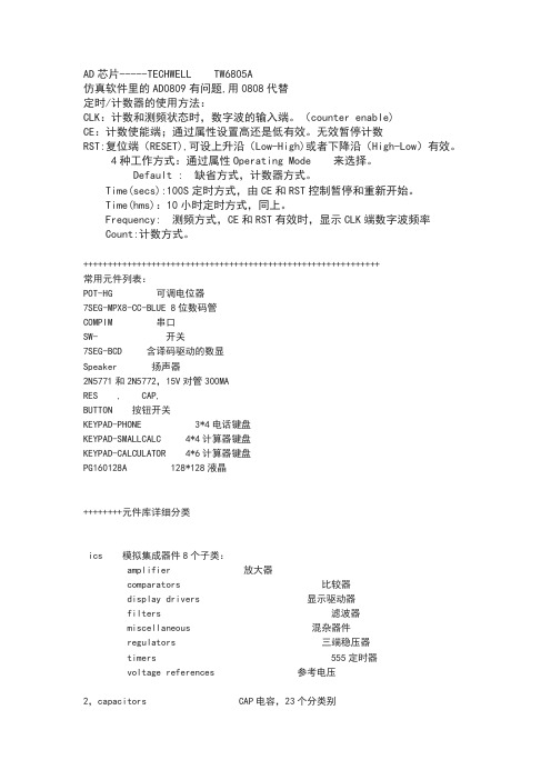
AD芯片-----TECHWELL TW6805A仿真软件里的AD0809有问题,用0808代替定时/计数器的使用方法:CLK:计数和测频状态时,数字波的输入端。
(counter enable)CE:计数使能端;通过属性设置高还是低有效。
无效暂停计数RST:复位端(RESET),可设上升沿(Low-High)或者下降沿(High-Low)有效。
4种工作方式:通过属性Operating Mode 来选择。
Default : 缺省方式,计数器方式。
Time(secs):100S定时方式,由CE和RST控制暂停和重新开始。
Time(hms):10小时定时方式,同上。
Frequency: 测频方式,CE和RST有效时,显示CLK端数字波频率Count:计数方式。
+++++++++++++++++++++++++++++++++++++++++++++++++++++++++++++常用元件列表:POT-HG 可调电位器7SEG-MPX8-CC-BLUE 8位数码管COMPIM 串口SW- 开关7SEG-BCD 含译码驱动的数显Speaker 扬声器2N5771和2N5772,15V对管300MARES , CAP,BUTTON 按钮开关KEYPAD-PHONE 3*4电话键盘KEYPAD-SMALLCALC 4*4计算器键盘KEYPAD-CALCULATOR 4*6计算器键盘PG160128A 128*128液晶++++++++元件库详细分类ics 模拟集成器件8个子类:amplifier 放大器comparators 比较器display drivers 显示驱动器filters 滤波器miscellaneous 混杂器件regulators 三端稳压器timers 555定时器voltage references 参考电压2,capacitors CAP电容,23个分类别animated 可显示充放电电荷电容audio grade axial 音响专用电容axial lead polypropene 径向轴引线聚丙烯电容axial lead polystyrene 径向轴引线聚苯乙烯电容ceramic disc 陶瓷圆片电容decoupling disc 解耦圆片电容high temp radial 高温径向电容high temp axial electrolytic高温径向电解电容metallised polyester film 金属聚酯膜电容metallised polypropene 金属聚丙烯电容metallised polypropene film 金属聚丙烯膜电容miniture electrolytic 微型电解电容multilayer metallised polyester film 多层金属聚酯膜电容mylar film 聚酯薄膜电容nickel barrier 镍栅电容non polarised 无极性电容polyester layer 聚酯层电容radial electrolytic 径向电解电容resin dipped 树脂蚀刻电容tantalum bead 钽珠电容variable 可变电容vx a xial electrolytic VX 轴电解电容3,CMOS 4000 series 4000系列数字电路adders 加法器buffers & drivers 缓冲和驱动器comparators 比较器counters 计数器decoders 译码器encoders 编码器flip-flops & latches 触发器和锁存器frequency dividers & tiner 分频和定时器gates & inverters 门电路和反相器memory 存储器混杂逻辑电路mutiplexers 数据选择器multivibrators 多谐振荡器phase-locked loops(PLL) 锁相环registers 寄存器signal switcher 信号开关4,connectors 接头;8个分类:audio 音频接头D-type D型接头DIL 双排插座header blocks 插头miscellaneous 各种接头PCB transfer PCB 传输接头SIL 单盘插座ribbon cable 蛇皮电缆terminal blocks 接线端子台5,data converters 数据转换器:4个分类:A/D converters 模数转换器D/A converters 数模转换器sample & hold 采样保持器temperature sensors 温度传感器6,debugging tools 调试工具数据:3个类别:breakpoint triggers 断点触发器logic probes 逻辑输出探针logic timuli 逻辑状态输入7,diodes 二极管;8个分类:bridge rectifiers 整流桥generic 普通二极管rectifiers 整流二极管schottky 肖特基二极管switching 开关二极管tunnel 隧道二极管varicap 稳压二极管8,inductors 电感:3个类别:generic 普通电感SMT inductors 表面安装技术电感transformers 变压器9,laplace primitives 拉普拉斯模型:7个类别:1st order 一阶模型2nd order 二阶模型controllers 控制器non-linear 非线性模型operators 算子poles/zeros 极点/零点symbols 符号10,memory ICs 存储器芯片:7个分类:dynamic RAM 动态数据存储器EEPROM 电可擦出程序存储器EPROM 可擦出程序存储器I2C memories I2C总线存储器memory cards 存储卡SPI Memories SPI总线存储器static RAM 静态数据存储器11,microprocessor ICs 微处理器:13个分类:12,modelling primitivvves 建模源:9个分类:13,operational amplifiers 运算放大器:7个分类:dual 双运放ideal 理想运放macromodel 大量使用的运放octal 8运放quad 4运放single 单运放triple 三运放14,optoelectronics 光电器件:11个分类:7-segment displays 7段显示alphanumeric LCDs 液晶数码显示bargraph displays 条形显示dot matrix displays 点阵显示graphical LCDs 液晶图形显示lamps 灯LCD controllers 液晶控制器LCD controllers 液晶面板显示LEDs 发光二极管optocouplers 光电耦合serial LCDs 串行液晶显示15,resistors 电阻:11个分类:metal film 金属膜电阻10 watt wirewound 10w绕线电阻2w metal film 2w 金属膜电阻3 watt wirewound 3w 绕线电阻7 watt wirewound 7w 绕线电阻generix 普通电阻high voltage 高压电阻NTC 负温度系数热敏电阻resistor packs 排阻variable 滑动变阻器varisitors可变电阻参考试验中采用的可变电阻是:POT-HG16,simulator primitives 仿真源:3个类别:flip-flops 触发器gates 门电路sources 电源17,switches and relays 开关和继电器:4个类别:key pads 键盘relays 普通继电器relays(specific) 专用继电器switches 开关18,switching devices 开关器件:4个分类:DIACs 两端交流开关generic 普通开关元件SCRs 可控硅TRIACs 三端双向可控硅19,真空管:20,传感器:2个分类:pressure 压力传感器temperature 温度传感器21,晶体管:8个分类:bipolar 双极型晶体管generic 普通晶体管(错误)IGBT 绝缘栅双极晶体管JFET 结型场效应管MOSFET 金属氧化物场效应管RF power LDMOS 射频功率LDMOS管RF power VDMOS 射频功率VDMOS管unijunction 单结晶体管Electromechanical 电机MOTOR AC 交流电机MOTOR SERVO 伺服电机双相步进电机motor-bistepper(Bipolar Stepper Motor),四相步进电机motor-stepper(unipolar stepper motor)驱动电路,用ULN2003可以,proteus中推荐的L298和L6201(电子元件-步进电机中有L298资料)+++++++++++++++++++++++++++++++++++++++++++++++++++++++++++++++++++++步进电机,可以用MTD2003,UN2916等专用芯片Proteus中图形液晶模块驱动芯片一览表LM3228 LM3229 LM3267 LM3283LM3287 LM4228 LM4265 LM4267LM4283 LM4287 PG12864F PG24064FPG128128A PG160128AAGM1232G EW12A03GLY HDM32GS12-B HDM32GS12Y-BHDG12864F-1 HDS12864F-3 HDG12864L-4 HDG12864L-6NOKIA7110 TG126410GFSB TG13650FEYAMPIRE128x64 LGM12641BS1RPROTEUS原理图元器件库详细说明单双向可控硅、包括电阻、电容、二极管、三极管和PCB的连接器符号、包括虚拟仪器和有源器件、拨动开关、键盘、可调电位器和开关、包括二极管和整流桥、稳压管、变容二极管、大功率二极管、高速二极管、可控硅、包括LCD、LED、LED阵列包括三极管包括场效应管包括模拟元器件AS 稳压二极管、全桥、74系列、及其他。
朗斯测试技术有限公司 Lance LC07系列内装IC应变加速度传感器用户手册说明书

Lance LC07系列LanceLC07系列内装IC应变加速度传感器用户手册朗斯测试技术有限公司LANCE MEASUREMENT TECHNOLOGIES CO.,LTD.目录一、概述 (2)二、技术指标·······································2三、使用方法及注意事项 (4)四、附件及随机文件 (13)全国销售电话:4008-824-824 更多资料详情:一、概述加速度的测量:在大于0.3Hz时,利用压电加速度传感器—电荷放大器测量系统或内装IC压电加速度传感器都可以进行理想的测量。
在小于0.3Hz时,通常使用应变加速度传感器—应变仪测量系统,但由于零漂和噪声都较大,特别在测量小加速度时,很难得到理想的测量结果。
LC07系列内装IC应变加速度传感器的出现,很好的解决了这一难题。
该系列传感器不同于传统的应变桥结构,它是在硅片上同时集成了42个对加速度敏感的可变电容单元,同时解决了零漂、噪声、精度三大难题。
二、技术指标主要技术指标型号量程g-3dB频响Hz灵敏度mV/g抗冲击g噪声密度mg/Hz轴向电源V/mALC0701-2±2DC-2500100020000.11单+5/1 LC0701-5±5DC-250030020000.15单+5/1 LC0702±18DC-250010020000.19单+5/3 LC0703±50DC-1000385001单+5/3 LC0704±100DC-4001910004单+5/3 LC0705±18DC-250010020000.19双+5/1 LC0706±50DC-1000385001双+5/5±10DC-6001905001三+5/7 LC0709±18DC-250010020000.19三+5/1注:1.内装IC应变加速度传感器有如下共同技术指标:·线性:0.5%·横向灵敏度:≤5%·输出短路:无限期·电缆长度:3米2.型号后缀A,电源为8-20V。
HB771S培训
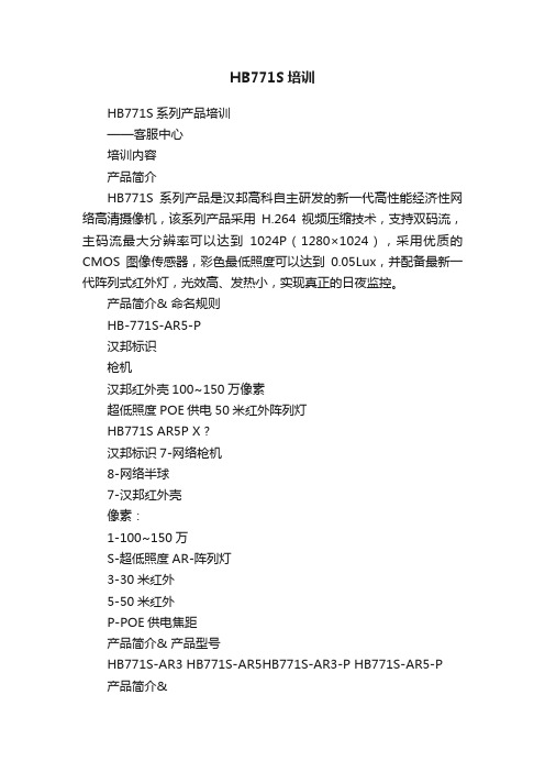
HB771S培训HB771S系列产品培训——客服中心培训内容产品简介HB771S系列产品是汉邦高科自主研发的新一代高性能经济性网络高清摄像机,该系列产品采用H.264视频压缩技术,支持双码流,主码流最大分辨率可以达到1024P(1280×1024),采用优质的CMOS图像传感器,彩色最低照度可以达到0.05Lux,并配备最新一代阵列式红外灯,光效高、发热小,实现真正的日夜监控。
产品简介& 命名规则HB-771S-AR5-P汉邦标识枪机汉邦红外壳100~150万像素超低照度POE供电50米红外阵列灯HB771S AR5P X ?汉邦标识7-网络枪机8-网络半球7-汉邦红外壳像素:1-100~150万S-超低照度AR-阵列灯3-30米红外5-50米红外P-POE供电焦距产品简介& 产品型号HB771S-AR3 HB771S-AR5HB771S-AR3-P HB771S-AR5-P产品简介&独特的外观设计配色:主体亮白色:防止夏天太阳直射导致机体温度过高。
配色暗灰色:防止光线反射。
采用汉邦私有红外摄像机壳,美观大气,铝合金材质让摄像机在提升散热性能的同时,具备了一定的防破坏能力。
工作温度-20℃~60℃,工作湿度小于90%(无凝结),配备防护罩,并且具有IP66的防水防尘等级,无论是晴天、雨天还是雪天都可以正常工作。
各部件连接紧密,连接处采用六角螺丝,防止拆卸。
顶部双螺丝设定,使防护罩在机身上更加稳固,不易晃动。
精心设计,打造优质产品。
产品简介& 多种供电方式可选DC12V ±10%POE供电产品简介& 图像质量高采用SONY 1/3英寸逐行扫描CMOS 图像传感器,图像分辨率最高可达1024P(1280×1024),有效像素高达140万,出来的图像效果更加动人。
图象清晰,细节更丰富。
通透性好,噪点少。
色彩还原准确。
产品简介& 夜视效果好采用最新一代阵列式红外灯,发光效率高,照射距离远,产生的热量小,使用寿命长。
TS9007_07资料

TS9007 300mA Low Noise CMOS LDOSOT-25DFN 2x2SOT-23General DescriptionThe TS9007 series is 300mA ultra-low-noise LDO especially designed for battery-power RF and wireless applications. The TS9007 regulator achieves a low 450mV dropout at 300mA load current of 3.3V output, ultra-low output voltage noise of 15uVrms and PSRR of 57dB at 1KHz.The TS9007 regulators are also optimized to work with low-ESR and low cost ceramic capacitors reducing the amount of board space critical in hand-held devices. The TS9007 requires only 0.47uF output capacitor for stability with and load. The TS9007 consumes less than 1uA in shutdown mode.Features● 450mV Dropout at 300mA load (3.3V) ● Low quiescent current: 90µA ● Output voltage ±2%● Internal current limit and thermal shutdown ● Power saving shutdown mode (<1uA) ● Only need input and output capacitors ● Build-In internal Soft-Start●Output short-circuit current limit protectionApplications● Palmtops, PDA and Notebook Computers ● DSC, Handset Camera Modules ● PCMCIA Cards, PC Cameras● USB Based Portable Devices (MPS, PMP) ●GSM/GPRS/3G RF Transceiver ModulesOrdering InformationNote: Wherex denotes voltage option, available are1= 1.2V A = 1.5V D = 1.8V K = 2.5V M = 2.7V N = 2.8V O = 2.9V P = 3.0V S = 3.3VContact factory for additional voltage options.Part No.PackagePackingTS9007x CX RF SOT-23 3Kpcs / 7” Reel TS9007x CX5 RF SOT-25 3Kpcs / 7” Reel TS9007x CQ RF DFN 2x2 3Kpcs / 7” Reel Block DiagramTypical Application CircuitEN (Pin 3) may be connected directly to V IN (Pin1) Low noise operation: C BYP =30nF, C OUT >0.47uF Basic operation: C BYP =not used, C OUT >1uFC OUT 0.47uF C BYP 30nFonoffEN V OUTV INPin Definition:1. Input2. Ground3. Enable4. Bypass5. OutputPin Definition: 1. Input 2. N/C 3. Output 4. N/C 5. Ground 6. EnablePin Definition:1. Ground2. Output3. InputTS9007 300mA Low Noise CMOS LDOAbsolute Maximum RatingParameterSymbolLimitUnitSupply VoltageV IN -0.3 ~ +7V Input Supply Voltage (Recommended) V OPR +2 ~ +6 V Output Short-Circuit DurationInfinitePower Dissipation SOT-25 300SOT-23 300DFN 2x2 P D 500 mWSOT-25 250SOT-23 300Thermal Resistance DFN 2x2 ӨJA 165°C/W Junction Temperature Range T J +150 °C Storage Temperature Range T STG -65 ~ +150 °CNotes: Stress above the listed absolute rating may cause permanent damage to the device.Electrical Characteristics (T A = 25o C, V IN = (V OUT +1V), C IN =C OUT =0.47uF, V EN =V IN , unless otherwise noted.)ParameterConditionsMinTypMaxUnitOutput Voltage V IN =V O + 1V, I O =10mA -2.0 -- +2 % Output Current Limit Short-circuit output-- 200 -- mA Maximum Output Current V IN =Vo+1V,300 -- -- mA Line Regulation V IN =(V OUT +1V) to 6V, I O =10mA -- 0.3 -- %/V V IN =Vo+1V, 1mA ≤IL ≤300mA V OUT ≥2.5V -- 0.2 1.0 Load RegulationV IN =Vo+1V, 1mA ≤IL ≤200mA V OUT <2.5V -- 0.2 1.0 %Io=300mA, V OUT =Vo - 2% V OUT ≥2.5V -- 500 600 Dropout Voltage Io=200mA, V OUT =Vo - 2% V OUT <2.5V-- 800 1000 mV Shutdown Supply Current EN=0V-- 0.01 -- uA Ground Pin Current Io=0mA-- 90 150 uA f=100Hz, Io=1mA-- 60 -- f=1KHz, Io=1mA -- 57 -- Ripple Rejection (PSRR)f=10Hz, Io=1mA-- 45 -- dBIo=10mA, f=10Hz to 100kHz, Bypass = 0nF-- 45 --Output NoiseIo=10mA, f=10Hz to 100kHz, Bypass = 30nF -- 15 -- uVrmsShutdown Exit Delay (note 2) R LOAD = 50Ω-- 45 300 uSEN Logic Low Level V IN =2.0V to 5.5V -- -- 0.4 EN Logic High LevelV IN =2.0V to 5.5V 1.5--VINV EN Input Bias Current V IN =2.0V to 5.5V-- -- -- uAThermal Shutdown Shutdown Temperature -- 160 -- o C Thermal Shutdown Hysteresis -- 20 -- oCNotes:a. The drop out voltage varies depending on output voltage selection.Dropout is defined as V IN - V OUT when V OUT is 100mV below V OUT where V IN = Vout+1V for nominal V OUTb. Time needed for V OUT to reach 90% of final valueTS9007300mA Low Noise CMOS LDOApplication InformationEnable / ShutdownThe TS9007 comes with and active-high enable pin that allows the regulator to be enabled. Forcing the enable pin low disables the regulator and puts it into the shutdown mode. This pin cannot be left floating as it may cause an undetermined state.Input / Output CapacitorIt is recommended to use a 0.47uF capacitor on the TS9007 input and a 0.47uF capacitor on the output. For high regulation performance, larger input capacitor values and lower ESRs provide better noise rejection and line-transient response. The output noise, load-transient response, stability, and power-supply rejection can be improved by using large output capacitors. Low ESR ceramic capacitors provide optimal performance and save space.Power Supply Rejection and Transient ResponseThe PSRR and transient response can be improved by increasing the values of the input and output bypass capacitors, and through passive filtering techniquesFunction DescriptionDescriptionThe TS9007 is an ultra-low-noise, low-quiescent current, low-dropout linear regulator. It is supplied in a SOT-25 package for difference applications. This device can supply loads up to 300mA. As shown in the functional block diagram, the TS9007 consists of a reference and noise bypass circuit, error amplifier, output drive transistor, internal feedback voltage divider, thermal sensor, and short circuit current limiter. The internal reference is connected to the error amplifier’s inverting input. The error amplifier compares this reference with the feedback voltage and amplifies the difference. If the feedback voltage is lower than the reference voltage, the pass=transistor gate is pulled low. This allows more current to pass to the output and increases the output voltage.StabilityThe TS9007 is a high performance LDO emphasizing stability with low output capacitance. It is able to maintain stability with an output capacitor can also be increased to optimize performance. The TS9007 will remain stable and in regulation with no load, unlike many other voltage regulators.Internal P-Channel Pass TransistorThe TS9007 features a low impedance P-channel MOSFET pass transistor. This provides several advantages over similar designs using a PNP pass transistor, including low operating power and longer battery life. The TS9007 consumes only 90µA of quiescent current under most conditions.Output Short-Circuit Current LimitThe TS9007 includes a current limiter, which monitors and controls the pass transistor’s gage voltage, limiting the output current to about 200mA, for example, in a short-circuit output situation.ShutdownThe TS9007 also features a low-power active shutdown mode. It has a switch that turns off the device when disabled. This allows the output capacitor and load to discharge and de-energize the load. In the shutdown mode, the internal functional blocks, such as voltage reference and the error amplifier, are turned off completely, and the quiescent current is less than 1µA.TS9007300mA Low Noise CMOS LDOFunction Description (Continue)Thermal Protection ShutdownThe thermal protection shutdown function protects the device from operating in over temperature condition. When the junction temperature exceeds +160o C, the thermal sensor signals the shutdown logic, turning off the pass transistor and allowing the IC to tool down. The thermal sensor turns the pass transistor on again after the IC’s junction temperature drops to +140o C.Soft-Start CircuitryThe TS9007 includes a soft-start circuitry to limit inrush current at turn-on. During power up, the output capacitor and output load are charged with a reduce output current. Shortly after the initial power up, the soft-start feature is terminated and normal operation is resumed.TS9007 300mA Low Noise CMOS LDOSOT-23 Mechanical DrawingMarking DiagramA = Device CodeX = Fixed Output Voltage Code1=1.2V, A =1.5V, D =1.8V, K =2.5V, M =2.7V, N =2.8V, O =2.9V P =3.0V, S =3.3V Y = Year Code M = Month Code(A =Jan, B =Feb, C =Mar, D =Apl, E =May, F =Jun, G =Jul, H =Aug, I =Sep, J =Oct, K =Nov, L =Dec) L = Lot CodeSOT-23 DIMENSION MILLIMETERS INCHES DIM MIN MAX MIN MAX. A 0.95 BSC 0.037 BSC A1 1.9 BSC 0.074 BSC B 2.60 3.00 0.102 0.118 C 1.40 1.70 0.055 0.067 D 2.80 3.10 0.110 0.122 E 1.00 1.30 0.039 0.051 F 0.00 0.10 0.000 0.004 G 0.35 0.50 0.014 0.020 H 0.10 0.20 0.004 0.008 I 0.30 0.60 0.012 0.024 J5º 10º 5º 10ºTS9007 300mA Low Noise CMOS LDOSOT-25 Mechanical DrawingMarking DiagramA = Device CodeX = Fixed Output Voltage Code1=1.2V, A =1.5V, D =1.8V, K =2.5V, M =2.7V, N =2.8V, O =2.9V P =3.0V, S =3.3V Y = Year Code M = Month Code(A =Jan, B =Feb, C =Mar, D =Apl, E =May, F =Jun, G =Jul, H =Aug, I =Sep, J =Oct, K =Nov, L =Dec) L = Lot CodeSOT-25 DIMENSIONMILLIMETERS INCHES DIM MIN MAX MIN MAX. A+A1 0.09 1.25 0.0354 0.0492 B 0.30 0.50 0.0118 0.0197 C 0.09 0.25 0.0035 0.0098 D 2.70 3.10 0.1063 0.1220 E 1.40 1.80 0.0551 0.0709 E 1.90 BSC 0.0748 BSC H 2.40 3.00 0.09449 0.1181 L 0.35 BSC 0.0138 BSC Ө1 0º 10º 0º 10º S10.95 BSC 0.0374 BSCTS9007 300mA Low Noise CMOS LDODFN 2x2 Mechanical DrawingMarking DiagramA = Device CodeX = Fixed Output Voltage Code1=1.2V, A =1.5V, D =1.8V, K =2.5V, M =2.7V, N =2.8V, O =2.9V P =3.0V, S =3.3V Y = Year Code M = Month Code(A =Jan, B =Feb, C =Mar, D =Apl, E =May, F =Jun, G =Jul, H =Aug, I =Sep, J =Oct, K =Nov, L =Dec) L = Lot CodeDFN 2x2 DIMENSION MILLIMETERS INCHES DIM MIN MAX MIN MAX A 0.25 0.35 0.0098 0.0138 a1 0.10 (typ) 0.0039 (typ) B 0.90 1.10 0.0354 0.0433 C 0.50 (typ) 0.0197 (typ) D 0.50 (typ) 0.0197 (typ) E 0.15 0.25 0.0059 0.0098 F 1.30 1.50 0.0512 0.0591 G 0.67 0.73 0.0264 0.0287 H 0.20 0.30 0.0079 0.0118 I 0.60 (MAX.) 0.0236 (MAX.) J 0.07 (MAX.) 0.0028 (MAX.) K 1.75 1.85 0.0689 0.0728 L1.952.05 0.0768 0.0807TS9007300mA Low Noise CMOS LDONoticeSpecifications of the products displayed herein are subject to change without notice. TSC or anyone on its behalf, assumes no responsibility or liability for any errors or inaccuracies.Information contained herein is intended to provide a product description only. No license, express or implied, to any intellectual property rights is granted by this document. Except as provided in TSC’s terms and conditions of sale for such products, TSC assumes no liability whatsoever, and disclaims any express or implied warranty, relating to sale and/or use of TSC products including liability or warranties relating to fitness for a particular purpose, merchantability, or infringement of any patent, copyright, or other intellectual property right.The products shown herein are not designed for use in medical, life-saving, or life-sustaining applications. Customers using or selling these products for use in such applications do so at their own risk and agree to fully indemnify TSC for any damages resulting from such improper use or sale.。
Skyworks Solutions 双DVB-C2 S2 S2X T C S数字电视解调器说明书

DescriptionThe Si21602C integrates two separate high-performance digital demodulators for the DVB-C2/C, DVB-T, DVB-S2/S and DVB-S2X standards into a single compact package. Leveraging Skyworks'proven digital demodulation architecture, the Si21602C achieves excellent reception performance for each media while significantly minimizing front-end design complexity, cost, and power dissipation. Connecting the Si21602C to both a dual terrestrial/cable TV tuner, and a dual satellite tuner, results in a high-performance and cost optimized TV front-end solution.Skyworks' internally developed DVB-C2 demodulator can accept a standard IF (36 MHz) or low-IF input (differential) and support all modes specified by the DVB-C2 standard. The main features of the DVB-C2 mode are 4096-QAM, 6 or 8MHz bandwidth,management of notch insertion (broadband and narrowband), and support of multiple data slices and PLPs.The DVB-T and DVB-C, including ITU-T J.83 annex B,demodulators are enhanced versions of proven and broadly used Si2164/67/68/69 Skyworks devices.The satellite reception allows demodulating widespread DVB-S,DIRECTV™ (DSS), DVB-S2, DIRECTV™ (AMC) legacy standards, and new Part II of DVB-S2 (S2X) satellite broadcast standard. A zero-IF interface (differential) allows for a seamless connection to market proven satellite silicon tuners. It also integrates two DiSEqC™ 2.0 LNB interfaces for satellite dish control and, for each satellite demodulator, an equalizer to compensate for echoes in long cable feeds from the LNB to the satellite tuner RF input.The Si21602C offers an on-chip blind scanning algorithm for DVB-S/S2/S2X and DVB-C standards, as well as blind lock function.Features-Pin-to-pin compatible with all dual demodulator family: Si216x2 and Si218x2-API compatible with all single and all dual demodulators -DVB-C2 (ETSI EN 302 769)-16-QAM to 4096-QAM OFDM demodulation -DVB-T (ETSI EN 300 744)-NorDig Unified 2.5, D-Book 8 compliant-DVB-C (ETSI EN 300 429) / ITU-T J.83 Annex A/B/C-1 to 7.2 MSymbol/s, C-Book compliant -DVB-S2 (ETSI EN 302 307-1 V1.4.1)-QPSK/8PSK demodulator-DVB-S2X (ETSI EN302 307-2 V1.1.1)-QPSK/8PSK, 8/16/32APSK demodulator -Roll-off factors from 0.05 to 0.35-Channel bonding for TS transmission supported -Dual DiSEqC™ 2.x interface, Unicable support -DVB-S (ETSI EN 300 421) and DSS supported - 1 to 45 MSps for all satellite standards (<40 MSps in 32APSK)-I 2C serial bus interfaces (master and host)-Upgradeable with firmware patch download via fast SPI or I 2C (broadcast mode supported)-Dual independent differential IF input for T/C tuners and differ -ential ZIF I/Q inputs for satellite tuners-GPIOs and multi-purpose ports (two per demodulator)-Separate flexible TS interfaces with serial or parallel outputs and cross-bar feature -Fast lock times for all standards-Only two power supplies: 1.2 and 3.3V8x8mm, QFN-68 pin package, Pb-free/RoHS compliantSelected Electrical Specifications (T A =–10 to 70°C).ParameterTest Condition Min Typ Max Unit GeneralInput clock reference 4—30MHz Supported XTAL frequency 16—30MHz T otal power consumption for each demodulatorDVB-T 1—182—mW DVB-C22—327—mW DVB-C 3—142—mW DVB-S24—421—mW DVB-S 5—230—mW Thermal resistance ( JA ) 4 layer PCB—42—°C/W Power Supplies V DD _VCORE 1.14 1.20 1.30V V DD _VANA 3.00 3.30 3.60V V DD _VIO3.003.303.60VNotes:1. T est conditions: 8MHz, 8K FFT, 64-QAM, parallel TS.2. T est conditions: 4096-QAM, CR =5/6, GI =1/128, C/N = 34 dB (at picture failure).3. T est conditions: 6.9Mbaud, 256-QAM, parallel TS.4. T est conditions: 32Mbaud, CR =3/5, 8PSK, pilots On, parallel TS, C/N at picture failure.5.T est conditions: 30Mbaud, CR =7/8, parallel TS, at QEF: BER =2 x 10⁻⁴.Pin AssignmentsSelection GuidePart #DescriptionSi21602-C60-GM/R Dual Digital TV Demodulator for DVB-C2/S2/S2X/T/C/S, 8x8mm QFN-68_A D C _I P _AD D R _AD D R _BD D _A N AOT A L _I /C L K _I NE S E T BD D _C O R EP _C _AP _D _BP I O _1/T S _E R R _AD D _C O R ES 2_D A T A [7]S 1_D A T A [6]S 2_D A T A [6]S 1_D A T A [7]S 2_D A T A [5]M P _A _AD I SE C _C M D _G P I O _0/T S _E R R _M P _B _BD I SE Q C _O U T _D I S E Q C _I N _A _D I S E Q C _O U T _G N DV D D _C O R EV D D _C O R ES C L _H O S TV D D _V I OS D A _H O S T T S 1_S Y N CT S 2_V A LT S 1_V A LT S 2_S Y N C。
- 1、下载文档前请自行甄别文档内容的完整性,平台不提供额外的编辑、内容补充、找答案等附加服务。
- 2、"仅部分预览"的文档,不可在线预览部分如存在完整性等问题,可反馈申请退款(可完整预览的文档不适用该条件!)。
- 3、如文档侵犯您的权益,请联系客服反馈,我们会尽快为您处理(人工客服工作时间:9:00-18:30)。
TO-92
SOT-89
PRODUCT SUMMARY
BV CBO -50V BV CEO -50V I C
-3A
V CE(SAT)
-0.5V @ I C / I B = -2A / -200mA
Features
● Low V CE(SAT) -0.25 @ I C / I B = 2A / 200mA (Typ.) ● Complementary part with TSD882S
Structure
● Epitaxial Planar Type ● PNP Silicon Transistor
Ordering Information
Part No.
Package
Packing
TSD772SCT B0 TO-92 1Kpcs / Bulk TSD772SCT A3 TO-92 2Kpcs / Ammo TSD772SCY RM
SOT-89
1Kpcs / 7” Reel
Absolute Maximum Rating (Ta = 25o C unless otherwise noted)
Parameter
Symbol
Limit
Unit
Collector-Base Voltage V CBO -50 V Collector-Emitter Voltage V CEO -50 V Emitter-Base Voltage V EBO -5 V DC -3 Collector Current
Pulse I C -7 (note) A SOT-89 0.75 Collector Power Dissipation
TO-92
P D 0.625 W
Operating Junction Temperature
T J +150 o
C Operating Junction and Storage Temperature Range T STG
- 55 to +150
o C
Note: Single pulse, Pw ≤350us, Duty ≤2%
Electrical Specifications (Ta = 25o C unless otherwise noted)
Parameter
Conditions
Symbol
Min
Typ
Max
Unit
Collector-Base Breakdown Voltage I C = -50uA, I E = 0 BV CBO -50 -- -- V Collector-Emitter Breakdown Voltage I C = -1mA, I B = 0 BV CEO -50 -- -- V Emitter-Base Breakdown Voltage I E = -50uA, I C = 0 BV EBO -5 -- -- V Collector Cutoff Current V CB = -30V, I E = 0 I CBO -- -- -1 uA Emitter Cutoff Current
V EB = 3V, I C = 0 I EBO -- -- -1 uA Collector-Emitter Saturation Voltage I C / I B = -2A / -200mA *V CE(SAT) -- -0.3 -0.5 V Base-Emitter Saturation Voltage I C / I B = -2A / -200mA
*V BE(SAT) -- -1 -2 V DC Current Transfer Ratio
V CE = -2V, I C = -1A *h FE 100 -- 500 Transition Frequency
V CE =-5V, I C =-100mA,
f=100MHz
f T -- 80 -- MHz Output Capacitance V CB = -10V, f=1MHz Cob
--
55
--
pF
* Pulse Test: Pulse Width ≤380uS, Duty Cycle ≤2%
Pin Definition: 1. Base 2. Collector 3. Emitter
Pin Definition: 1. Emitter
2. Collector
3. Base
Electrical Characteristics Curve (Ta = 25o C, unless otherwise noted)
Figure 1. DC Current Gain
Figure 2. V CE(SAT) v.s. Ic
Figure 3. V BE(SAT) v.s. Ic
Figure 4. Power Derating Curve
TO-92 Mechanical Drawing
TO-92 DIMENSION
MILLIMETERS INCHES
DIM
MIN MAX MIN MAX
A 4.30 4.70 0.169 0.185
B 4.30 4.70 0.169 0.185
C 14.30(typ) 0.563(typ)
D 0.43 0.49 0.017 0.019
E 2.19 2.81 0.086 0.111
F 3.30 3.70 0.130 0.146
G 2.42 2.66 0.095 0.105
H 0.37 0.43 0.015 0.017
SOT-89 Mechanical Drawing
SOT-89 DIMENSION
MILLIMETERS INCHES DIM
MIN MAX MIN MAX
A 4.40 4.60 0.173 0.181
B 1.50 1.7 0.059 0.070
C 2.30 2.60 0.090 0.102
D 0.40 0.52 0.016 0.020
E 1.50 1.50 0.059 0.059
F 3.00 3.00 0.118 0.118
G 0.89 1.20 0.035 0.047
H 4.05 4.25 0.159 0.167
I 1.4 1.6 0.055 0.068 J 0.35 0.44 0.014 0.017
Notice
Specifications of the products displayed herein are subject to change without notice. TSC or anyone on its behalf, assumes no responsibility or liability for any errors or inaccuracies.
Information contained herein is intended to provide a product description only. No license, express or implied, to any intellectual property rights is granted by this document. Except as provided in TSC’s terms and conditions of sale for such products, TSC assumes no liability whatsoever, and disclaims any express or implied warranty, relating to sale and/or use of TSC products including liability or warranties relating to fitness for a particular purpose, merchantability, or infringement of any patent, copyright, or other intellectual property right.
The products shown herein are not designed for use in medical, life-saving, or life-sustaining applications. Customers using or selling these products for use in such applications do so at their own risk and agree to fully indemnify TSC for any damages resulting from such improper use or sale.。