BYV12中文资料
RM12中文资料
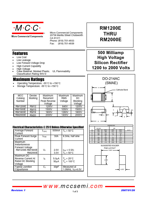
RM1200E THRU RM2000E500 Milliamp High Voltage Silicon Rectifier 1200 to 2000 VoltsFeatures• Low Cost • Low Leakage• Low Forward Voltage Drop • High Current Capability • High VoltageMaximum Ratings• Operating Temperature: -55°C to +150°C •Storage Temperature: -55°C to +150°CMCC Catalog Number Device Marking Maximum Recurrent Peak Reverse Voltage Maximum RMS Voltage Maximum DC Blocking Voltage RM1200E 1200V 840V 1200V RM1500E 1500V 1050V 1500V RM1800E 1800V 1260V 1800V RM2000E2000V1400V 2000VElectrical Characteristics @ 25°C Unless Otherwise SpecifiedAverage Forward CurrentI F(AV)500mA T A = 50°C Peak Forward Surge Current I FSM30A8.3ms, half sineMaximum Instantaneous Forward VoltageRM1200E-RM1800ERM2000EV F 2.0V 3.0V I FM = 0.5A;T A = 50°C Maximum DCReverse Current At Rated DC Blocking VoltageI R 5.0µA 50µA T A = 25°C T A = 100°C Typical Junction CapacitanceC J30pFMeasured at1.0MHz, V R =4.0Vomp onents 20736 Marilla Street Chatsworth! "# $ % ! "#Micro Commercial ComponentsxCase Material: Molded Plastic. UL Flammability Classification Rating 94V-0www.mccsemi .comRM12RM15RM18RM20RM1200E - RM2000E110040510158Figure 3Peak Forward Surge Current Peak Forward Surge Current - Amperes versus Number Of Cycles At 60Hz - CyclesAmpsCycles261020608040202530Instantaneous Reverse Current - Micro Amps versus Percent Of Rated Peak Reverse Voltage - VoltsFigure 1Typical Reverse Characteristics 012020406080.01.02.04.06T J = 25°CµAVolts100.08.1.2.4.6.8124Average Forward Rectified Current - Amperes versus Ambient Temperature - °CFigure 2Forward Derating Curve150255075100100200300Single Phase, Half Wave60Hz Resistive or Inductive Load mA°C125400500600TMMicro Commercial Componentswww.mccsemi .comMicro Commercial Components***IMPORTANT NOTICE***Micro Commercial Components Corp.reserve s the right to make changes without further notice to any product herein to make corrections, modifications , enhancements , improvements , or other changes .Micro Commercial Components Corp.does not assume any liability arising out of the application or use of any product described herein; neither does it convey any license under its patent rights ,northe rights of others . The user of products in such applications shall assume all risks of such use and will agree to hold Micro Commercial Components Corp.and all the companies whoseproducts are represented on our website, harmless against all damages.***APPLICATIONS DISCLAIMER***Products offer by Micro Commercial Components Corp.are not intended for use in Medical,Aerospace or Military Applications.。
AV106-12中文资料
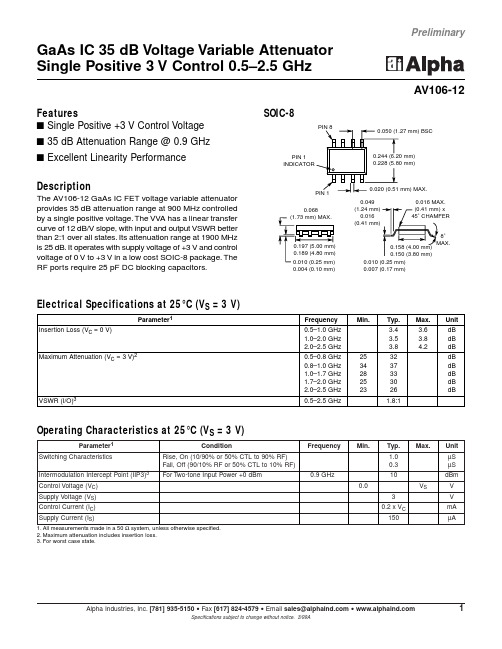
Parameter 1ConditionFrequency Min.Typ.Max.Unit Switching CharacteristicsRise, On (10/90% or 50% CTL to 90% RF) 1.0µS Fall, Off (90/10% RF or 50% CTL to 10% RF)0.3µS Intermodulation Intercept Point (IIP3)3For Two-tone Input Power +0 dBm0.9 GHz10dBmControl Voltage (V C )0.0V SV Supply Voltage (V S )3V Control Current (I C ) 0.2 x V C mA Supply Current (I S )150µAGaAs IC 35 dB Voltage Variable Attenuator Single Positive 3 V Control 0.5–2.5 GHzFeaturess Single Positive +3 V Control Voltage s 35 dB Attenuation Range @ 0.9 GHz s Excellent Linearity PerformanceSOIC-8AV106-120.0490.016 MAX.0.004 (0.10 mm)0.007 (0.17 mm)8˚PIN 1DescriptionThe AV106-12 GaAs IC FET voltage variable attenuator provides 35 dB attenuation range at 900 MHz controlled by a single positive voltage.The VVA has a linear transfer curve of 12 dB/V slope, with input and output VSWR better than 2:1 over all states.Its attenuation range at 1900 MHz is 25 dB.It operates with supply voltage of +3 V and control voltage of 0 V to +3 V in a low cost SOIC-8 package.The RF ports require 25 pF DC blocking capacitors.Electrical Specifications at 25°C (V = 3 V)Operating Characteristics at 25°C (V S = 3 V)1.All measurements made in a 50 Ωsystem, unless otherwise specified.2.Maximum attenuation includes insertion loss.3.For worst case state.Preliminary2.52.0Frequency (GHz)Insertion Loss vs. FrequencyI n s e r t i o n L o s s (d B )0.51.01.5-5.0-4.5-4.0-3.5-3.0-2.5-20.-1.5-1.0-0.50.02.52.03.01.5V C (V)Attenuation vs. Control VoltageA t t e n u a t i o n (dB )0.51.0-40-35-30-25-20-15-10-50 2.502.00Frequency (GHz)Maximum Attenuation vs. FrequencyM a x i m u m A t t e n u a t i o n (d B )0.501.001.50-40-35-30-25-20-15-10-50Typical Performance Data @ 0.9 GHz(Unless Otherwise Specified)V C (V)VSWR vs. Control VoltageV S W R1.01.11.21.31.41.51.61.71.81.92.02.52.03.01.50.51.02.02.53.01.5V C (V)Input IP3 vs. Control VoltageI I P 3 (d B m )0.51.051015202530 2.0 2.5 3.01.5V C (V)Attenuation vs. Control VoltageOver TemperatureI n s e r t i o n L o s s (d B )0.5 1.0-5-4-3-2-1012345J 2CharacteristicValue RF Input Power 50 mW > 500 MHzSupply Voltage +7 V Control Voltage +3.3 V Operating Temperature -40°C to +85°C Storage Temperature -65°C to +150°CΘJC25°C/WAbsolute Maximum RatingsPin OutDC blocking capacitors (C BL ) supplied externally.C BL = 25 pF for operation >500 MHz.Note:Exceeding these parameters may cause irreversible damage.。
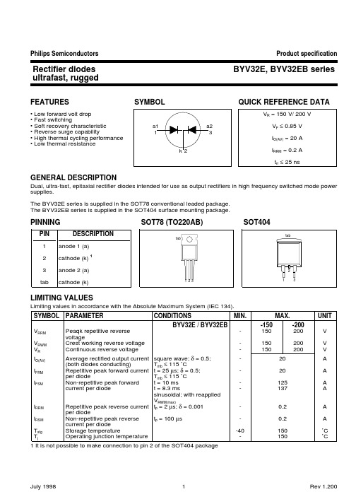
BYV32中文资料

BYV32,BYVF32 & BYVB32 SeriesVishay Semiconductorsformerly General SemiconductorDocument Number Reverse Voltage 50 to 200VForward Current 18AReverse Recovery Time25nsMounting Pad Layout TO-263ABITO-220AB (BYVF32 Series)TO-220AB (BYV32 Series)TO-263AB (BYVB32 Series)Features• Plastic package has Underwriters Laboratory Flammability Classification 94V-0• Dual rectifier construction, positive centertap • Glass passivated chip junctions • Low power loss• Low forward voltage, high current capability • High surge current capability• Superfast recovery times for high efficiencyMechanical DataCase:JEDEC TO-220AB, ITO-220AB & TO-263AB molded plastic bodyTerminals:Plated leads, solderable per MIL-STD-750, Method 2026High temperature soldering guaranteed:250°C, 0.16" (4.06mm) from case for 10 seconds Polarity:As marked Mounting Position:Any Mounting Torque:10 in-lbs maximum Weight:0.08 oz., 2.24 gBYV32,BYVF32 & BYVB32 SeriesVishay Semiconductorsformerly General Semiconductor Document Number 88558Maximum Ratings (TC= 25°C unless otherwise noted)ParameterSymbol BYV32-50BYV32-100BYV32-150BYV32-200Unit Maximum repetitive peak reverse voltage V RRM 50100150200V Maximum RMS voltage V RMS 3570105140V Maximum DC blocking voltageV DC 50100150200V Maximum average forward rectified current at T C = 125°C I F(AV)18A Peak forward surge current8.3ms single half sine-wave superimposed I FSM 150A on rated load (JEDEC Method) per legOperating junction and storage temperature range T J , T STG –65 to +150°C RMS Isolation voltage (BYVF type only) from terminals to 4500 (1)heatsink with t = 1.0 second, RH ≤30%V ISOL3500 (2)V1500 (3)Electrical Characteristics (TC= 25°C unless otherwise noted)ParameterSymbol BYV32-50BYV32-100BYV32-150BYV32-200Unit Maximum instantaneous forward voltage per leg at:(4)at I F = 20AV F1.15Vat I F = 5.0A,T J = 100°C 0.85Maximum DC reverse current per leg T J = 25°C 10at rated DC blocking voltageT J = 100°CI R 600µA Maximum reverse recovery time per leg atI F = 1A, V R = 30V , di/dt = 100A/µs, I rr = 10% I RM t rr 25ns Typical junction capacitance per leg at 4V , 1MHzC J45pFThermal Characteristics (TC= 25°C unless otherwise noted)ParameterSymbol BYV BYVF BYVB Unit Thermal resistance from junction to case per legR ΘJC1.65.01.6°C/WNotes:(1) Clip mounting (on case), where lead does not overlap heatsink with 0.110”offset (2) Clip mounting (on case), where leads do overlap heatsink(3) Screw mounting with 4-40 screw, where washer diameter is ≤4.9mm (0.19”)(4) Pulse test:300µs pulse width, 1% duty cycleBYV32,BYVF32 & BYVB32 SeriesVishay Semiconductorsformerly General SemiconductorDocument Number Ratings andCharacteristic Curves (T A = 25°C unless otherwise noted)I F – I n s t a n t a n e o u s F o r w a r d C u r r e n t (A )1001010.10.01Maximum Non-Repetitive Peak Forward Surge Current Per Leg4.01618208.0A v e r a g e F o r w a r d R e c t i f i e d C u r r e n t (A )1211010010020********Reverse Voltage (V)p F – J u n c t i o n C a p a c i t a n c eForward Current Derating Curve。
AT45DB321-CC中文资料

SECTOR 0
BLOCK AR 1 BLOCK 2
8 Pages
SECTOR 1
SECTOR 2 = 270,336 bytes (256K + 8K)
BLOCK 62 BLOCK 63 BLOCK 64 BLOCK 65
SECTOR 2
SECTOR 15 = 270,336 bytes (256K + 8K) SECTOR 16 = 270,336 bytes (256K + 8K)
Read
By specifying the appropriate opcode, data can be read from the main memory or from either one of the two data buffers.
MAIN MEMORY PAGE READ: A main memory read allows the user to read data directly from any one of the 8192 pages in the main memory, bypassing both of the data buffers and leaving the contents of the buffers unchanged. To start a page read, the 8-bit opcode, 52H, is followed by 24 address bits and 32 don’t care bits. In the AT45DB321, the first address bit is reserved for larger density devices (see Notes on page 10), the next 13 address bits (PA12-PA0) specify the page address, and the next 10 address bits (BA9-BA0) specify the starting byte address within the
BYV32E-150 -200中文资料
-
per diode
Non-repetitive peak reverse tp = 100 µs
-
current per diode
Storage temperature
-40
Operating junction temperature
-
1 It is not possible to make connection to pin 2 of the SOT404 package
PF / W 10
Vo = 0.7 V Rs = 0.0183 Ohms
8
6
BYV32 2.8
Tmb(max) / C 126
1.9
2.2
a = 1.57
130.8
4 135.6
4
140.4
2
145.2
0
150
0
2
4
6
8
10
IF(AV) / A
Fig.6. Maximum forward dissipation PF = f(IF(AV)) per diode; sinusoidal current waveform where a = form
Product specification
BYV32E, BYV32EB series
ESD LIMITING VALUE
SYMBOL PARAMETER
VC
Electrostatic discharge
capacitor voltage
CONDITIONS
Human body model; C = 250 pF; R = 1.5 kΩ
factor = IF(RMS) / IF(AV).
12N60中文资料
Fig. 3A Gate Charge Test Circuit
Fig. 3B Gate Charge Waveform
10V
RD tp
L VDS
BVDSS IAS
VDD
VDD D.U.T.
ID(t) tp
VDS(t) Time
Fig. 4A Unclamped Inductive Switching Test Circuit Fig. 4B Unclamped Inductive Switching Waveforms
25℃ 100
55℃
10-1 2
Notes:
1.VDS=50V 2.250μs Pulse Test
4
6
8
10
Gate-Source Voltage, VGS (V)
UNISONIC TECHNOLOGIES CO., LTD
12N60-x-TF3-T
12N60L-x-TF3-T
Note: Pin Assignment: G: Gate D: Drain S: Source
Package
TO-220 TO-220F
Pin Assignment
1
2
3
G
D
S
G
D
S
Packing
Tube Tube
Copyright © 2008 Unisonic Technologies Co., Ltd
Turn-On Rise Time Turn-Off Delay Time
tR tD(OFF)
VDD = 300V, ID = 12A, RG = 25Ω (Note 4, 5)
115 240 nsቤተ መጻሕፍቲ ባይዱ95 200 ns
BY329-1000中文资料
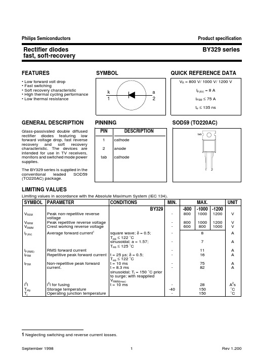
Philips Semiconductors Product specificationRectifier diodes BY329 seriesfast, soft-recoveryFEATURESSYMBOL QUICK REFERENCE DATA• Low forward volt drop • Fast switching• Soft recovery characteristic• High thermal cycling performance • Low thermal resistanceGENERAL DESCRIPTIONPINNINGSOD59 (TO220AC)Glass-passivated double diffused PIN DESCRIPTION rectifier diodes featuring low forward voltage drop,fast reverse 1cathode recovery and soft recovery characteristic.The devices are 2anode intended for use in TV receivers,monitors and switched mode power tabcathodesupplies.The BY329series is supplied in the conventional leaded SOD59(TO220AC)package.LIMITING VALUESLimiting values in accordance with the Absolute Maximum System (IEC 134).SYMBOL PARAMETERCONDITIONSMIN.MAX.UNIT BY329-800-1000-1200V RSM Peak non-repetitive reverse -80010001200V voltageV RRM Peak repetitive reverse voltage -80010001200V V RWM Crest working reverse voltage -6008001000V I F(AV)Average forward current 1square wave; δ = 0.5;-8A T mb ≤ 122 ˚Csinusoidal; a = 1.57;-7A T mb ≤ 125 ˚CI F(RMS)RMS forward current-11A I FRM Repetitive peak forward current t = 25 µs; δ = 0.5;-16A T mb ≤ 122 ˚CI FSMNon-repetitive peak forward t = 10 ms -75A current.t = 8.3 ms-82Asinusoidal; T j = 150 ˚C prior to surge; with reapplied V RWM(max)I 2t I 2t for fusing t = 10 ms -28A 2s T stg Storage temperature-40150˚C T jOperating junction temperature-150˚C1tab21 Neglecting switching and reverse current losses.Philips Semiconductors Product specificationRectifier diodes BY329 seriesfast, soft-recoveryTHERMAL RESISTANCESSYMBOL PARAMETERCONDITIONSMIN.TYP.MAX.UNIT R th j-mb Thermal resistance junction to -- 2.0K/W mounting baseR th j-aThermal resistance junction to in free air.-60-K/WambientSTATIC CHARACTERISTICST j = 25 ˚C unless otherwise stated SYMBOL PARAMETER CONDITIONS MIN.TYP.MAX.UNIT V F Forward voltage I F = 20 A- 1.5 1.85V I RReverse currentV R = V RWM ; T j = 125 ˚C-0.11.0mADYNAMIC CHARACTERISTICST j = 25 ˚C unless otherwise stated SYMBOL PARAMETERCONDITIONSMIN.TYP.MAX.UNIT t rr Reverse recovery time I F = 1 A; V R > 30 V; -dI F /dt = 50 A/µs -100135ns Q sReverse recovery chargeI F = 2 A; V R > 30 V; -dI F /dt = 20 A/µs -0.50.7µC dI R /dtMaximum slope of the reverse I F = 2 A; -dI F /dt = 20 A/µs-5060A/µsrecovery currentPhilips Semiconductors Product specificationRectifier diodes BY329 seriesfast, soft-recoveryPhilips Semiconductors Product specificationRectifier diodes BY329 seriesfast, soft-recoveryPhilips Semiconductors Product specificationRectifier diodes BY329 seriesfast, soft-recoveryMECHANICAL DATANotes1. Refer to mounting instructions for TO220 envelopes.2. Epoxy meets UL94 V0 at 1/8".Philips Semiconductors Product specification Rectifier diodes BY329 series fast, soft-recoveryDEFINITIONSData sheet statusObjective specification This data sheet contains target or goal specifications for product development. Preliminary specification This data sheet contains preliminary data; supplementary data may be published later. Product specification This data sheet contains final product specifications.Limiting valuesLimiting values are given in accordance with the Absolute Maximum Rating System (IEC 134). Stress above one or more of the limiting values may cause permanent damage to the device. These are stress ratings only and operation of the device at these or at any other conditions above those given in the Characteristics sections ofthis specification is not implied. Exposure to limiting values for extended periods may affect device reliability. Application informationWhere application information is given, it is advisory and does not form part of the specification.© Philips Electronics N.V. 1998All rights are reserved. Reproduction in whole or in part is prohibited without the prior written consent of the copyright owner.The information presented in this document does not form part of any quotation or contract, it is believed to be accurate and reliable and may be changed without notice. No liability will be accepted by the publisher for any consequence of its use. Publication thereof does not convey nor imply any license under patent or other industrial or intellectual property rights.LIFE SUPPORT APPLICATIONSThese products are not designed for use in life support appliances, devices or systems where malfunction of these products can be reasonably expected to result in personal injury. Philips customers using or selling these products for use in such applications do so at their own risk and agree to fully indemnify Philips for any damages resulting from such improper use or sale.。
CADSTAR V12中文版教程
CADSTAR V12培训手册Z UK E N株式会社图研中国代表处二〇一一年七月目录Cadstar 软件配臵 (3)安装步骤 (3)软件组成及设计流程 (4)示例描述 (5)设计步骤 (5)1.库编辑器 (5)原理图符号库(Symbol) (5)元件封装库(Component) (8)器件库(Part) (9)2.绘制原理图 (13)基本设臵 (13)绘制过程 (15)转换数据到PCB (21)3.绘制PCB版图 (22)基本设臵 (22)放臵元件 (25)网络优化 (27)双向设计更新 (28)多电源、地结构 (30)设臵布线参数 (31)4.自动布线器 (32)设臵操作环境 (33)检查布通率指数 (35)交互式布线、优化 (36)后处理操作 (39)返回PCB (42)5.加工数据输出 (42)设臵输出层 (42)输出光绘数据 (43)输出钻孔数据 (46)附录 (48)CADSTAR配臵操作系统:WindowsXP SP1、Vista、Win 7C P U :硬盘:内存:分辨率:1280 x 1024虚拟内存:CD-ROM:安装步骤1.插入Cadstar 安装光盘,自动运行安装引导界面,或者运行光盘根目录下\setup.exe程序。
2.选择安装部件。
3.指定安装目录,如C:\CADSTAR 12.1。
4.选择单机锁定方式(需安装软件狗驱动程序)或网络浮动方式(指定作口令服务器的机器),完成安装后重新启动计算机。
5.针对单机版或者网络版软件,分别设臵软件license.dat文件(此步骤由Zuken公司工程师现场协助安装)。
6.选择相应模块运行。
软件风格介绍Cadstar是Windows风格软件,实行所看即所得。
可以将所看到的sch或pcb内容存成一个color文件。
出gerber时也是将这些color文件按gerber的格式输出。
软件文件介绍∙Colours- this is where the Batch Process option looks for Colours files (used for setting up the WYSIWYG);∙Initial Design Directory - this is the default Working directory for your designs;∙Macros - this is where the system stores Macro files;∙Manufacturing Output - this is where the Batch Process option stores output Spool files;∙Datasheet Files - this is where HTML Datasheets for parts are generated (.htm);∙Report Generator Files- this is where the Batch Process option looks for files created by the Manage Reports option (.rgf files);∙Reuse Files- this is the default location where the system looks for and stores Reuse files;∙Selections- this is where the Batch Process option looks for Selections files (Scale and Position Plot etc.);∙Simulation Libraries - this is where the Signal Integrity tool looks for the Parts and the Models libraries it uses in design analysis;∙Templates- this where the system stores the pre-defined template files, from which you select when starting new designs/symbols/components;∙User- this is where the Batch Process option looks for Device files (r, r etc.);软件模块组成及设计流程软件模块Library Editor (库编辑器)Design Editor (原理图编辑器、PCB版图编辑器) PREditor XR (无网格自动布线器)EMC Adviser (电磁兼容专家分析系统)设计流程图示例描述本手册以“模拟计数器”为例,讲述利用Cadstar软件进行设计的全过程,内容包括器件库的建立(符号、封装及综合)、层次化原理图设计、PCB版图编辑及布局、自动布线及后处理、加工数据输出等。
- 1、下载文档前请自行甄别文档内容的完整性,平台不提供额外的编辑、内容补充、找答案等附加服务。
- 2、"仅部分预览"的文档,不可在线预览部分如存在完整性等问题,可反馈申请退款(可完整预览的文档不适用该条件!)。
- 3、如文档侵犯您的权益,请联系客服反馈,我们会尽快为您处理(人工客服工作时间:9:00-18:30)。
Electrical Characteristics
Tj = 25_C Parameter Forward voltage Reverse current Reverse recovery time Reverse recovery charge Test Conditions IF=1A VR=VRRM VR=VRRM, Tj=150°C IF=0.5A, IR=1A, iR=0.25A IF=1A, di/dt=5A/ms Type Symbol VF IR IR trr Qrr Min Typ 1 60 Max 1.5 5 150 300 200 Unit V mA mA ns nC
94 9522
tp – Pulse Length ( s )
Figure 8. Thermal Response
Dimensions in mm
∅ 3.6 max. Sintered Glass Case SOD 57 Weight max. 0.5 g Cathode Identification
Figure 6. Max. Forward Current vs. Forward Voltage
www.vishay.de • FaxBack +1-408-970-5600 2 (4)
Document Number 86039 Rev. 2, 24-Jun-98
元器件交易网
technical drawings according to DIN specifications 94 9538
∅ 0.82 max.
26 min.
4.2 max.
26 min.
Document Number 86039 Rev. 2, 24-Jun-98
www.vishay.de • FaxBack +1-408-970-5600 3 (4)
tp=10ms, half sinewave ϕ=180°, Tamb=25°C
Maximum Thermal Resistance
Test Conditions l=10mm, TL=constant on PC board with spacing 25mm Symbol RthJA RthJA Value 45 100 Unit K/W K/W
TL=constant
94 9101
l – Lead Length ( mm )
Figure 1. Typ. Thermal Resistance vs. Lead Length
1.2 I FAV– Average Forward Current ( A )
Figure 4. Junction Temperature vs. Reverse/Repetitive Peak Reverse Voltage
R thJA – Therm. Resist. Junction / Ambient ( K/W ) 120 T j – Junction Temperature (° C ) l 100 80 60 40 20 0 0 5 10 15 20 25 30
94 9517
240 l RthJA=100K/W 200 VR RM 160 BYV12 120 BYV14 80 BYV13 40 0 1000 0 200 400 600 800 VR,VRRM – Reverse / Repetitive Peak Reverse Voltage ( V ) BYV15 BYV16 VR
v v
10
1
Tj = 175°C
0.1
Tj = 25°C
0.01 0 1 2 3 4 Tamb – Ambient Temperature ( °C ) VF – Forward Voltage ( V )
94 9518
Figure 3. Max. Average Forward Current vs. Ambient Temperature
元器件交易网
BYV12...BYV16
Vishay Telefunken
Fast Silicon Mesa Rectifiers
Features
D D D D
Glass passivated junction Hermetically sealed package Soft recovery characteristic Low reverse current
Figure 5. Reverse Current vs. Junction Temperature
100
2.0 IF – Forward Current ( A ) 1.6 1.2 0.8 0.4 0 0 40 80 120 160 z RthJA 45K/W L=10mm
Applications
Fast rectifier and switch for example for TV–line output circuits and switch mode power supply
94 9539
Absolute Maximum Ratings
Tj = 25_C Parameter Reverse voltage g =Repetitive peak reverse voltage Test Conditions Type BYV12 BYV13 BYV14 BYV15 BYV16 Symbol VR=VRRM VR=VRRM VR=VRRM VR=VRRM VR=VRRM IFSM IFRM IFAV Tj=Tstg Value 100 400 600 800 1000 40 9 1.5 –65...+175 Unit V V V V V A A A °C
Peak forward surge current Repetitive peak forward current Average forward current Junction and storage temperature range Tj = 25_C Parameter Junction ambient
1000 I R – Reverse Current ( mA )
1.0 0.8 0.6 0.4 0.2 0 0 40 80
VR RM f 20kHz RthJA 100K/W PCB
v v
Scattering Limit 100
10
1 VR = VR RM 0 40 80 120 160 200
0.1 120 160 200
BYV12...BYV16
Vishay Telefunken
12 CD – Diode Capacitance ( pF ) 10 8 6 4 2 0 0.1
94 9523
f = 470kHz Tj = 25°C 1 10 100
VR – Reverse Voltage ( V )
Figure 7. Typ. Diode Capacitance vs. Reverse Voltage
Z thp – Thermal Resistance for Pulse Cond. (K/W) 1000 VR RM= 1000 V RthJA=100K/W 100 Tamb= 25°C Tamb= 45°C 10 Tamb= 60°C
Tamb= 70°C 1 10–5 Tamb= 100°C 10–4 10–3 10–2 10–1 100 101 100 101 IFRM – Repetitive Peak Forward Current ( A )
94 9521
94 9519
Tamb – Ambient Temperature ( °C )
Tj – Junction Temperature ( °C )
Figure 2. Max. Average Forward Current vs. Ambient Temperature
I FAV– Average Forward Current ( A )
Document Number 86039 Rev. 2, 24-Jun-98
www.vishay.de • FaxBack +1-408-970-5600 1 (4)
元器件交易网
BYV12...BYV16
Vishay Telefunken Characteristics (Tj = 25_C unless otherwise specified)
元器件交易网
BYV12...BYV16
Vishay Telefunken Ozone Depleting Substances Policy Statement
It is the policy of Vishay Semiconductor GmbH to 1. Meet all present and future national and international statutory requirements. 2. Regularly and continuously improve the performance of our products, processes, distribution and operating systems with respect to their impact on the health and safety of our employees and the public, as well as their impact on the environment. It is particular concern to control or eliminate releases of those substances into the atmosphere which are known as ozone depleting substances ( ODSs ). The Montreal Protocol ( 1987 ) and its London Amendments ( 1990 ) intend to severely restrict the use of ODSs and forbid their use within the next ten years. Various national and international initiatives are pressing for an earlier ban on these substances. Vishay Semiconductor GmbH has been able to use its policy of continuous improvements to eliminate the use of ODSs listed in the following documents. 1. Annex A, B and list of transitional substances of the Montreal Protocol and the London Amendments respectively 2 . Class I and II ozone depleting substances in the Clean Air Act Amendments of 1990 by the Environmental Protection Agency ( EPA ) in the USA 3. Council Decision 88/540/EEC and 91/690/EEC Annex A, B and C ( transitional substances ) respectively. Vishay Semiconductor GmbH can certify that our semiconductors are not manufactured with ozone depleting substances and do not contain such substances.