MIC5400YWM中文资料
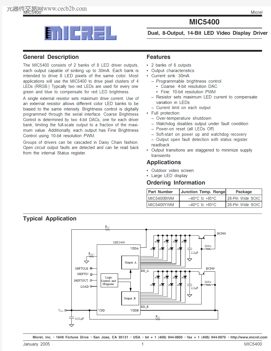
Typical Application
V DD
Micrel, Inc. ? 1849 Fortune Drive ? San Jose, CA 95131 ? USA ? tel + 1 (408) 944-0800 ? fax + 1 (408) 944-0970 ? https://www.360docs.net/doc/119191610.html,
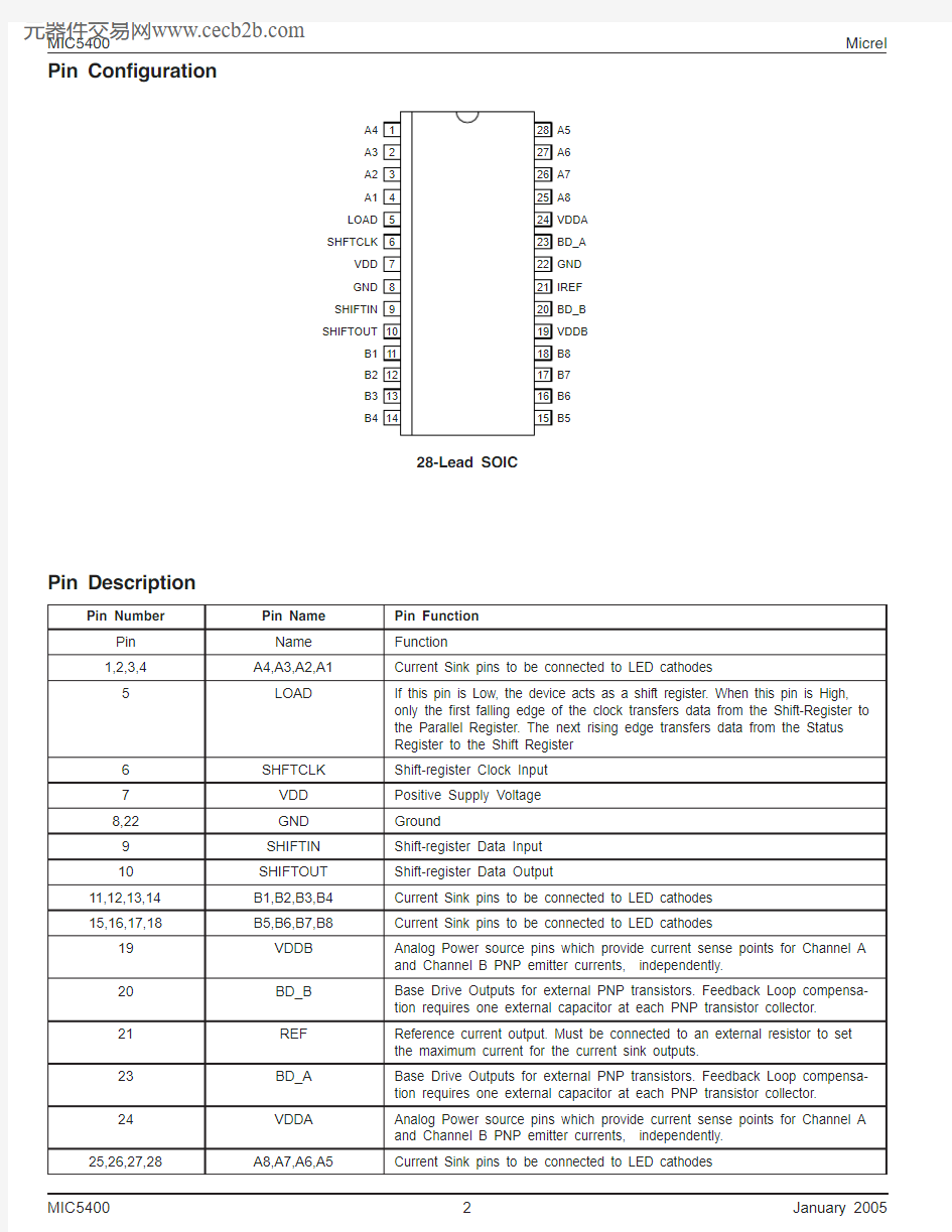
Pin Description
Pin Number
Pin Name Pin Function Pin Name Function
1,2,3,4A4,A3,A2,A1
Current Sink pins to be connected to LED cathodes
5
LOAD
If this pin is Low, the device acts as a shift register. When this pin is High,
only the first falling edge of the clock transfers data from the Shift-Register to the Parallel Register. The next rising edge transfers data from the Status Register to the Shift Register 6SHFTCLK Shift-register Clock Input 7VDD Positive Supply Voltage 8,22GND Ground
9SHIFTIN Shift-register Data Input 10SHIFTOUT Shift-register Data Output
11,12,13,14B1,B2,B3,B4Current Sink pins to be connected to LED cathodes 15,16,17,18
B5,B6,B7,B8Current Sink pins to be connected to LED cathodes
19VDDB Analog Power source pins which provide current sense points for Channel A and Channel B PNP emitter currents, independently.
20BD_B Base Drive Outputs for external PNP transistors. Feedback Loop compensa-tion requires one external capacitor at each PNP transistor collector.21REF Reference current output. Must be connected to an external resistor to set the maximum current for the current sink outputs.
23BD_A Base Drive Outputs for external PNP transistors. Feedback Loop compensa-tion requires one external capacitor at each PNP transistor collector.24VDDA Analog Power source pins which provide current sense points for Channel A and Channel B PNP emitter currents, independently.25,26,27,28
A8,A7,A6,A5
Current Sink pins to be connected to LED cathodes
Pin Configuration
A4A3A2A1LOAD SHFTCLK VDD GND SHIFTIN SHIFTOUT A5A6A7A8VDDA BD_A GND IREF BD_B VDDB B1B8B2B7B3B6B4B5
28-Lead SOIC
Absolute Maximum Ratings (Note 1)
Supply Voltage (7)
Input Voltage.......................................–0.3V to V CC + 0.3V Base Drive Voltage. (7)
Output Sink Current (per output)................................35mA Lead Temperature (soldering, 5 sec)........................260°C Junction Temperature (T J)(max)...............................125°C Operating Ratings (Note 2)
Supply Voltage (V CC)................................+4.75V to +5.5V Junction Temperature (T J).......................–40°C to +125°C Package Thermal Resistance
SOIC (θJC).......................................................... 28°C/W SOIC (θJA).........................................................100°C/W
DC Electrical Characteristics
V DD = 4.75V to 5.5 V, T A = 25°C, bold values indicate –40°C ≤ T A≤ +85°C. R BIAS = 500?. Applies to all channels unless noted. Symbol Parameter Condition Min Typ Max Units I OUT Output Sink Current2635mA ?I OUT Output Current Matching7% I OUT(OFF)Output Off Leakage V OUT = 5V–11μA I DD Supply Current V DD = 5.5V02mA I B PNP Base Drive Current V BD = 4V750mA V REF Reference Output Voltage I REF = –4mA 1.9 2.1V V IH Logic 1 Input Threshold 2.2V V IL Logic 0 Input Threshold0.8V V OH Logic 1 Output Level I LOAD = 1mA 2.4V V OL Logic 0 Output Level I LOAD = 1mA0.4V T SHUTDOWN Thermal Shutdown Temperature165°C
AC Electrical Characteristics
V DD = 4.75V to 5.5V, T A = 25°C, bold values indicate –40°C ≤ T A≤ +85°C. R BIAS = 500?. Applies to all channels unless noted Symbol Parameter Conditions Min Typ Max Units f SHIFT Shift Frequency15MHz t SET-DATA Set Up Time for Data In Note 57ns t HOLD-DATA Hold Time for Data In Note 513ns t SET-LOAD Set Up Time for Load Note 520ns t HOLD-LOAD Hold Time for Load Note 513ns I OUT(tr)Rise Time I OUT Note 4, 5125ns I OUT(ttf)Fall Time I OUT Note 4, 550ns t D-SHIFT Clock to Shift Out Delay Rise and Fall, 50% C LOAD = 30pF, Note 523ns t r,f-OUT Shift Out Rise and Fall Time10% to 90%; C LOAD =30pF, Note 510ns t WD-TIMEOUT Watch Dog Timeout Delay No Shiftclock25200μs t r,f[in]Logic Input Rise and Fall Times10ns Note 1.Exceeding the absolute maximum rating may damage the device.
Note 2.The device is not guaranteed to function outside its operating rating.
Note 3.Devices are ESD sensitive. Handling precautions recommended. Human body model, 1.5k in series with 100pF.
Note 4.Test circuit shown in Figure 1.
Note 5.Guaranteed by design; not production tested.
Test Circuit
V OUT to FET Probe (C < 1.5pF)
V DD = 5V
Figure 1.AC Output Test Circuit
Timing Diagrams
SHFTCLK
LOAD
Control Register Contents
Shift Register Contents Status Register Contents
Figure 2.MIC5400 Timing Diagram
Linearity
5
10
15202530354045
I O U T ( m A )
I REF (mA)
Typical Global Full Scale Linearity
(any output)
Figure 3.Typical Global Full Scale Linearity
Functional Diagram
SHIFTIN
SHFTCLK
MIC5400 Functional Diagram
Address Data A Data B Watchdog Divisor DAC B DAC B
3 Bits10 bits10 Bits 1 Bit
4 Bits 4 Bits 4 Bits
Q1 to Q3Q4 to Q13Q14 to Q23Q24Q25 to Q28Q29 to Q32Q33 to Q36 [Q1 = LSB]
Bit Description
1Address bit 1
2Address Bit 2
3Address Bit 3
4Data A Bit 1
5Data A Bit 2
6Data A Bit 3
7Data A Bit 4
8Data A Bit 5
9Data A Bit 6
10Data A Bit 7
11Data A Bit 8
12Data A Bit 9
13Data A Bit 10
14Data B Bit 1
15Data B Bit 2
16Data B Bit 3
17Data B Bit 4
18Data B Bit 5
19Data B Bit 6
20Data B Bit 7
21Data B Bit 8
22Data B Bit 9
23Data B Bit 10
24Watchdog Bit [Disable = 1]
25Divisor Bit 1
26Divisor Bit 2
27Divisor Bit 3
28Divisor Bit 4
29DAC A Bit 1
30DAC A Bit 2
31DAC A Bit 3
32DAC A Bit 4
33DAC B Bit 1
34DAC B Bit 2
35DAC B Bit 3
36DAC B Bit 4
Table 1. Shift Register Data Format
Status A Status B Watchdog Thermal Mask Revision Alternating Bits [1 = Open Circuit][1 = Open Circuit][1 = Timeout][1 = Overtemp]
8 Bits8 Bits 1 Bit 1 Bit 3 Bits15 Fixed Bits
D1-D8D9-D16D17D18D19 to D21D22 to D36
Bit Description
1Status A - Bit 1 (Output Open Circuit = 0)
2Status A - Bit 2 (Output Open Circuit = 0)
3Status A - Bit 3 (Output Open Circuit = 0)
4Status A - Bit 4 (Output Open Circuit = 0)
5Status A - Bit 5 (Output Open Circuit = 0)
6Status A - Bit 6 (Output Open Circuit = 0)
7Status A - Bit 7 (Output Open Circuit = 0)
8Status A - Bit 8 (Output Open Circuit = 0)
9Status B - Bit 1 (Output Open Circuit = 0)
10Status B - Bit 2 (Output Open Circuit = 0)
11Status B - Bit 3 (Output Open Circuit = 0)
12Status B - Bit 4 (Output Open Circuit = 0)
13Status B - Bit 5 (Output Open Circuit = 0)
14Status B - Bit 6 (Output Open Circuit = 0)
15Status B - Bit 7 (Output Open Circuit = 0)
16Status B - Bit 8 (Output Open Circuit = 0)
17Watchdog Status [0 = Normal, 1 = Time Out]
18Thermal Status [0 = Normal, 1 = Overtemp]
19Mask Revision Bit 1
20Mask Revision Bit 2
21Mask Revision Bit 3
220 [Fixed Pattern Filler Bits]
231
240
251
260
271
280
291
300
311
320
331
340
351
360
Table 2. Status Word Format
Applications Information
Output Current Drive
The MIC5400 includes several ways to program LED output current. These output current controls are superimposed and have an additive effect on LED output current as follows:Global Full Scale Current Limit:
This function sets the Global Full Scale (GFS) current at each of the outputs. The G FS value current is about 8.1 times ISET.ISET is the current through the single resistor, RBIAS,connected from VREF to Ground. VREF is regulated to 2V (nominal) so:
I V R V R SET REF BIAS BIAS =
=()2 and GFS V R BIAS
=[]×[]812.For R BIAS = 500?, GFS = ≈32.4mA
The recommended value for I SET is 4mA or less for linear operation. See Figure 3.Brightness Control
Brightness contol is provided by two, 4-bit DACs, one DAC for each of the two output banks of 8 outputs. The output current is varied between 0*GFS and (15/16) *GFS in 15 equal steps based on the 4 Bit DAC code from the shift register Data Word; Bits Q29 -Q32 control Output Bank A and Bits QA33-36 control Output Bank B. (See Table 1: Data Word Format).Watchdog Status is read back from Status Word Bit Q17.Thermal Status is read from Status Word Bit Q18.Output Intensity
Each LED Output intensity is further controlled by a Pulse Width Modulator providing 10-bit resolution intensity varia-tion. One LED output per bank can be set up for each Data Word. A 3-bit address selects 1 of the 8 PWMs for each of the two output banks. Programming bits Q1-Q3 determine the PWM address, bits Q4-Q13 control the PWMs driving Bank A, bits Q14-Q23 control the PWMs driving Bank B. The PWM is created by comparing the count of a 10-bit counter with the 10-bit programming word. If the count output is greater than the programming word, the output is “OFF”.
The PWM frequency is also programmable, in ratio to the frequency of the shift register clock. The ratio value is set by the Divisor, loaded into bits Q25-Q28 of the Data Word. See Table 3.
Watchdog and Thermal Shutdown
The MIC5400 incorporates both a watchdog and thermal shutdown.
The watchdog shuts off all outputs and sets watchdog
status bit to logic 1 if the shift clock is absent for more than 200 microseconds. Watchdog status remains logic 0 for shift clocks more frequent than 25 microseconds. The watchdog is enabled by data word bit Q24. Watchdog status is read back from status word bit D17.
As a result of the 25 microsecond minimum watchdog timeout delay, the lower limit of clock frequency is 40kHz.The thermal shutdown typically activates if the die tem-perature exceeds 165°C. Thermal shutdown shuts off all outputs and sets the Thermal status bit to logic 1 if over-temperature is detected. Thermal status is read back from status word bit D18.
External PNP Transistors
The external PNPs have a dual role. As part of a voltage regulator loop they aid in limiting package power dissipation.Sensing current in the PNP emitters also allows setting an overall limit to the current available to one bank of 8 LEDs.Power dissipation: The regulator loop controls the voltage at the LED drive output to limit power dissipation. The outputs are typically controlled to 1.1V. A 2.2 μF capactor is required at the collector of each PNP for frequency compensation.PNP Current Limit
The current limit of the external PNP can be set by conncting a sense resistor R CS from VDD to VDDA and VDDB respec-tively. The current limit is:
I LIM = 48mV
R
SC
If current limit is not used, short VDDA and VDDB to VDD.Daisy Chains
Parts may be cascaded in groups of arbitrary size. The SHIFTOUT pin of one part is connected to the SHIFTIN pin of the following part. Data bit 36 is the first bit data to be shifted in. Status bit 36 is the first status bit to be shifted out. (See Table 1 and Table 2)
When loading the 36-bit data words, the user must keep track of the number of SHIFTCLOCK cycles to determine when data is aligned for transfer to the control and PWM registers.For example, if one daisy chains 10 parts, 360 SHIFTCLK cycles are required to clock in all the data words.LOAD and the Data/Control and Status Registers:
When LOAD is low, the MIC5400 acts as a 36-bit shift register. When LOAD goes high, the part no longer shifts data. Data is transferred from the Shift Register to the parallel control registers on the first falling edge of SHIFTCLK after LOAD goes high. While LOAD remains high, the next rising edge of SHIFTCLOCK transfers data from the status regis-ters to the shift register. The first status bit to appear on SHIFTOUT is Status Filler Bit 36 (Logic 0). See Table 2 for description and Figure 2 for timing.
Status A or Status B = 0 if the output is open circuit, i.e., open LED.
After LOAD returns low, normal shift register operation re-sumes and status data is shifted out as new data words are shifted in on the rising edge of SHIFTCLK.
Divisor Code 0123456789A B C D E F Divide by R 12345678910111213141516Table 3. PWM Clock Ratio to Shift Clock [PWM Clock Freq. = (Shift Clock Freq)/R]
TIME (2.5ns/div)
(2V /d i v )
(1V /d i v
)TIME (2.5ns/div)
(1V /d i v )
TIME (2.5ns/div)
(1V /d i v
)
Output Current Sink Rise Time Clock to Shiftout Delay Time
Output Current Sink Fall Time
Package Information
Rev. 02
28-Pin Wide SOIC
MICREL, INC.1849 FORTUNE DRIVE SAN JOSE, CA95131USA
TEL + 1 (408) 944-0800 FAX + 1 (408) 944-0970 WEB https://www.360docs.net/doc/119191610.html,
The information furnished by Micrel in this datasheet is believed to be accurate and reliable. However, no responsibility is assumed by Micrel for its use.
Micrel reserves the right to change circuitry and specifications at any time without notification to the customer.
Micrel Products are not designed or authorized for use as components in life support appliances, devices or systems where malfunction of a product can reasonably be expected to result in personal injury. Life support devices or systems are devices or systems that (a) are intended for surgical implant into the body or (b) support or sustain life, and whose failure to perform can be reasonably expected to result in a significant injury to the user. A Purchaser’s use or sale of Micrel Products for use in life support appliances, devices or systems is at Purchaser’s own risk and Purchaser agrees to fully indemnify
Micrel for any damages resulting from such use or sale.
? 2005 Micrel, Incorporated.