(DA14580_bootloader)官方手册
DA14580如何添加配对密码

= user_app_on_tk_exch_nomitm,
.app_on_irk_exch
= NULL,
.app_on_csrk_exch
= NULL,
.app_on_ltk_exch
= default_app_on_ltk_exch,
.app_on_pairing_succeded
= user_app_on_pairing_succeeded,
2
中电港 钟志峰
#if (BLE_APP_SEC) void user_app_on_tk_exch_nomitm(uint8_t connection_idx, struct gapc_bond_req_ind const *param); void user_app_on_encrypt_req_ind(uint8_t connection_idx, struct gapc_encrypt_req_ind const *param); void user_app_on_pairing_succeeded(void); #endif // BLE_APP_SEC
// By default we send hardcoded oob data uint8_t oob_tk[KEY_LEN] = APP_SECURITY_OOB_TK_VAL;
app_easy_security_tk_exch(connection_idx, (uint8_t*) oob_tk, KEY_LEN); } #else default_app_on_tk_exch_nomitm(connection_idx, param); #endif }
DA14580蓝牙智能系统级芯片(SoC)

DA14580蓝牙智能系统级芯片(SoC)推出的号称全球功率最低、体积最小的SmartBond DA14580智能系统级芯片(),与竞争计划相比,该产品可将搭载应用的智能型手机配件,或计算机周边商品的电池巡航时光延伸一倍。
DA14580简介:Dialog推出的号称全球功率最低、体积最小的SmartBond DA14580蓝牙智能系统级芯片(SoC),与竞争计划相比,该产品可将搭载应用的智能型手机配件,或计算机周边商品的电池巡航时光延伸一倍。
该款芯片的设计目的是透过无线方式将键盘、鼠标或遥控器与平板计算机、笔记型计算机或智能电视户相衔接;让消费者能够透过智能型手机和平板计算机上的各种创新应用,与手表、护腕或智能卷标建立衔接,实现如“自我评测”健康和身体情况,和寻觅遗失的钥匙等各种功能。
SmartBond是首款突破4mA无线收发极限的蓝牙智能解决计划,能够让设计人员将产品的电池续航时光延伸一倍,或缩减所需电池的数量和大小。
其独特的低功率架构的无线收发电流仅消耗3.8mA,比市场上其它蓝牙智能解决计划低50%,而且其深度睡眠模式的电流低于600nA。
这表示在一个每秒发送20字节的产品中,一颗 225mAh纽扣电池可以让其持续运作4年5个月;与此相比,前几代蓝牙智能技术仅能维持2年时光。
DA14580拥有一个功率管理区块,内含一个DC-DC转换器以及全部须要的,从而降低对外部组件以及总物料清单的需求。
透过精准地打开和关闭每个芯片块的供电,Dialog能够将功耗降至最低。
SmartBond 的运作可降低至此前所未有的0.9V,从而实现用法一颗碱性电池或镍锰电池就能运作计算机或智能电视周边商品,而过去则需要两颗电池。
这为设计人员放开了通往很多新设计思路的大门,让他们能够开发出超紧密和新尺寸的产品,同时降低系统的总成本。
能源采集技术,如采集到的光能或动能,也可以用于对支持系统运作的可充电电池举行充电。
第1页共5页。
DA14580 SUOTA在IOS平台的使用方法

BD0006-DA14580 SUOTA在IOS平台的使用方法文档版本:v0.0.4本文只介绍在IOS下用SUOTA APP给DA14580升级新程序,关于DA14580的img 文件怎么制作,怎么烧录到DA14580,请查阅其他文章。
SUOTA需要DA14580外挂1Mbits以上的FLASH或者EEPROM,当然DA14583不需要,因为它已经内置了1M FLASH。
本文的演示需要用到事先制作好的img文件,关于img文件怎么制作,请查看我的其他文档。
这里再啰嗦一点,除了用IOS升级,也可以用Android,当然,官方的文档说Android 会不稳定。
这里我们以IOS版SUOTA为例:当然,先别急着打开APP,在此之前,我们要把要升级的img文件拷贝到手机。
工具可以选择iTunes或者iTools,其道理是一样的,这里以iTools为例,将手机连上iTools,然后选择:打开SUOTA的文件共享,并选择以下文件夹,将要升级的文件拷贝到该文件夹下,这里我拷贝了3个文件,可以根据自己的需求来拷,反正升级只需要一个:拷贝完毕后关闭iTools,断开手机。
然后打开手机APP,点击搜索,之前请让DA14580工作在广播状态。
不一会儿,就会出现SUOTA02这个设备,这是我们事先烧录好的程序(相关方法请查阅我的其他文档,下文不再重复说明),点击SUOTA02与设备建立连接。
点击Update,选择fw03.img(SUOTA02是fw02.img,所以我们选择新的)。
正常的话会出现以下界面:由于我们用的是FLASH,所以选择SPI,然后根据自己的硬件选择SPI口的配置,关于Image bank,可以选择Oldest-自动选择老的区块覆盖,Bank1-覆盖区块1,Bank2-覆盖区块2,Block size-一般选择默认好了,完毕后点击Send to device。
然后出现以下界面:等待它升级完成,会跳出以下界面:选择reboot,再刷新界面,可以看到更新后的设备—SUOTA03:说明更新成功。
DA14580 蓝牙模块

蓝牙4.1 低功耗BLE 模块YH-001_V1.01(主芯片Dialog_ DA14580)模块概述YH-001_V1.01 是一个蓝牙4.1 单模低功耗(BLE)数传模块,高度集成了蓝牙低功耗射频、协议栈、profile 以及应用程序于系统级芯片DA14580 (内置蓝牙+ARMcortex-M0),它不仅无需外接MCU,而且提供足够的I/O 用于硬件设计和程序开发,非常适合应用于需要超低功耗的系统上。
主要特性1.蓝牙4.1 单模低功耗模块2.完美支持主从模式(Master/Slave)3.集成蓝牙低功耗BLE 协议栈16MHz/32bit ARM Cortex M0,无需要外接MCU4.内置AES-128bit 加密程序5.内置专用链路层处理器6.射频特性TX 功率:-20dBm 至0dBm RX 灵敏度:-93dBm7.通信传输有效距离:30M(无外置功放)8.处理器16MHz 32 位ARM Cortex M0,带有SWD 接口9.内存32kB 的一次性可编程(OTP)闪存42K SRAM 84kB ROM 8kB 保留SRAM10. 工作电压典型值3.0V 建议范围 2.5V-3.3V (支持普通7 号、5 号和纽扣电池供电)11. RF 收发器3V 供电,理想状态TX:3.4mA RX:3.7mA12. 接口4 通道10 位ADC 2 个UART 接口SPI 接口I2C 接口PWM 输出20 通用I/O 接口13. 封装尺寸23.2mm * 17mm * 1.8mm应用领域:1.医疗保健设备2.运动及健康设备3.家庭智能设备4.手机和PC 配件5.工业自动化设备6. 物联网节点设备及网关7. 智能遥控器(含语音识别)8. 手机APP 控制互动玩具9. 手机APP 控制四轴飞行器10.HID 外设,键盘、鼠标……YH-001_V1.01 方框图YH001-V1.01电气特性:绝对最大额定值建议工作条件NOTE1:基于蓝牙芯片RAM 工作特性,要求蓝牙设备冷启动时VDD ≧2.5 V,所以建议模块供电稳定VDD=3V外形尺寸:YH-001_V1.01 的总体尺寸,长23.2 毫米,宽17 毫米,厚1.8 毫米。
DA14580学习总结

DA14580学习汇总简介芯片名称:DA14580内核:Cortex-M0 32-bit系统时钟:16MHZ 睡眠时钟:32K (所以要外挂两个晶振)协议栈:不开源,采用Riviera Waves授权协议栈IPRam:42 kB System SRAM(存放运行数据)8 kB RetentionSRAM(低漏电存储器,暂存休眠状态下的运行数据)存储方式:32k的OTP(一次性烧录),要实现反复烧录则需要外挂一个flash或者EEPROM 84 kBROM(存放协议栈)最小系统只需7个元件支持仿真烧录方式:串口烧录(JTAG也可以烧录,烧录到外挂的芯片中)封装:34 pins,40pins, 48 pins功耗:首款突破4mA无线收发电流极限的蓝牙智能解决方案(小米手环可满足30天续航)术语Profile:配置文件(在GATT的基础上进行数据的本地处理)GATT:Generic Attribute Profile 通用的配置文件(负责基础的数据通信)DISS:设备信息服务(显示设备的制造商信息)UUID:全球唯一识别码,如0x2A45位设备序列号的UUID(任意蓝牙都可以通过他获取到设备序列号)。
AES:Advanced Encryption Standard 是DA14580中内置的128 位加密处理器development_guide:开发手册GAP:Generic Access Profile 通用接口配置。
跟蓝牙的advertising相关GTL: Generic Transport Layer 通用传输层。
当工作于外部主控模式时,用来传输主控到DA14580的数据NVDS: Non-Volatile Data Storage 非易失性数据存储器OTP: One Time Programmable (memory) 单次可编程存储器PHY:physical layer物理层LL:Link Layer链路层外挂EEPROMDA14580的芯片是没有flash空间的(其实有个32kb的OTP,但只能烧写一次),也可以使用烧录到内存,但是掉电过后就没有程序了。
BLE-DA14580-Part-9-Da14580
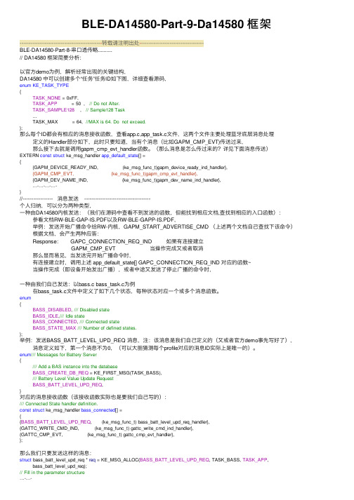
BLE-DA14580-Part-9-Da14580 框架----------------------------------------------转载请注明出处------------------------------------BLE-DA14580-Part-8-串⼝透传略..........// DA14580 框架简要分析:以官⽅demo为例,解析经常出现的关键结构,DA14580 中可以创建多个“任务”任务ID如下图,详细查看源码,enum KE_TASK_TYPE{TASK_NONE = 0xFF,TASK_APP = 50 , // Do not Alter.TASK_SAMPLE128 , // Sample128 Task...TASK_MAX = 64, //MAX is 64. Do not exceed.};那么每个ID都会有相应的消息接收函数,查看app.c,app_task.c⽂件,这两个⽂件主要处理蓝⽛底层消息处理定义的Handler部分如下,此时只要知道,当有个消息(⽐如GAPM_CMP_EVT)传送过来,那么接下去就是调⽤gapm_cmp_evt_handler函数。
(那么消息是怎么传过来的?详见下⾯消息传送)EXTERN const struct ke_msg_handler app_default_state[] ={{GAPM_DEVICE_READY_IND, (ke_msg_func_t)gapm_device_ready_ind_handler},{GAPM_CMP_EVT, (ke_msg_func_t)gapm_cmp_evt_handler},{GAPM_DEV_NAME_IND, (ke_msg_func_t)gapm_dev_name_ind_handler},…-…-…-…-}//----------------- 消息发送 -------------------------------------个⼈归纳,可以分为两种类型,⼀种由DA14580内核发送:(我们在源码中查看不到发送的函数,但能找到相应⽂档,查找到相应的⼊⼝函数):参看⽂档RW-BLE-GAP-IS.PDF以及RW-BLE-GAPP-IS.PDF,举例:发送开始⼴播命令给RW-内核,GAPM_START_ADVERTISE_CMD (上述两个⽂档⾃⼰查找下该命令)根据⽂档,会产⽣两种应答:Response: GAPC_CONNECTION_REQ_IND 如果有连接建⽴GAPM_CMP_EVT 当操作完成⼜或者取消那么显⽽易见,当发送完开始⼴播命令时,有连接建⽴时,调⽤上述 app_default_state[] GAPC_CONNECTION_REQ_IND 对应的函数~当操作完成(即设备开始发出⼴播),或者中途⼜发送了停⽌⼴播的命令时,⼀种由我们⾃⼰发送:以bass.c bass_task.c为例在bass_task.c⽂件中定义了如下⼏个状态,每种状态对应⼀个或多个消息函数。
DA14580官方培训资料中文版5
…personal…portable…connectedDialog SDK 5.0.3 培训材料5–配对,绑定和安全2016.6BLE安全特性概览自定义服务源码讨论输出结果我们一起做一个demo…在我们开始前,我们建议你…看一下培训材料2关于自定义服务的应用 你将会从这个培训里面学到…基本理解BLE的安全特性和问题什么是配对?什么是绑定?‘Just-Works(立即工作)’配对方式单设备绑定基本理解多设备绑定如何在自定义服务数据库里加入配对接下来…看一下这份PPT的参考文档部分通用接入服务的低功耗安全特性和注意事项•在BLE通信中的相关安全特性考虑:•Man-in-the-Middle (MITM)MITM模式要求攻击者有能力去监听和改变传往通信链路中的信息。
一个例子是主动监听,攻击者会对被攻击设备发起独立主动的连接,并传递消息,使得设备相信自己是在一条私有连接上在进行通信。
攻击者可以理解所有往来交互的信息,并有能力加入额外的消息。
对应MITM的攻击,保护方式主要是使用万能钥匙的配对方式,或者使用带外配对的方式。
通用接入服务的低功耗安全特性•在BLE通信中的相关安全特性考虑:•被动监听被动监听是私下接收配对数据,或者没有配对下的普通交互数据;然后在没有得到同意的情况下(用sniffer工具)监听。
BLE v4.0针对这种情况没有保护机制(在BLE v4.2的安全连接特性里会采用ECDH的公共密钥来应对这种被动监听攻击—不在此次讨论范围之内)•隐私/身份追踪BLE支持隐私特性,会在一段时间内更新蓝牙地址,降低被跟踪的风险。
这种修改后的地址叫做私有地址,被信任的设备可以解析地址。
通入接入服务低功耗绑定•为了消除MITM和被动监听攻击带来的风险,两个BLE设备间需要进行配对.•配对是这样一个过程,两个设备间交互安全和身份信息,创建一种信任关系.•这些安全和身份信息就是所谓的绑定信息。
当设备开始存储这些绑定信息,意味着绑定已经建立,或者设备间已经被绑定在一起•一旦秘钥交互后,每一次的连接结束之后都会存储这些绑定信息。
DA14580中基于SDK5.03的SUOTA使用方法
BD0005-基于SDK5.03的SUOTA使用方法文档版本:v0.0.1DA14580开发的蓝牙产品,很多情况下要用到空中升级,本文介绍了如何使用SUOTA,并如何利用Dongle更新新版本程序,本文只针对SDK5.0.3版本,后续有版本更新请参考新的文档。
DA1458x的空中升级需要对编译好的hex文件做适当处理,本文以SDK5.0.3为例,为您演示DA14580芯片如何制作和烧录SUOTA程序,要成功使用SUOTA,芯片外部必须外挂1M以上FLASH,我这里使用的是2Mbits SPI FLASH。
首先,我们有以下两个工具,第一个hex2bin是将hex文件转换为bin文件,第二个是制作SUOTA 的img文件,hex2bin是网上找的,如果你有类似的工具也可以使用,mkimage(关于这两个工具,的源码可以在SDK5.0.3中找到,用VC编译后可生成exe文件。
需要的话可以在附录中的地址下载到)这里我们以SDK5.0.3中的prox_reporter工程为例,首先打开工程:这里我们要生成两个版本的hex文件,fw01.hex和fw02.hex,作为两个不同版本的程序。
首先找到以下位置:修改设备名称为SUOTA01,作为第一个hex,编译并生成hex,找到刚生成的hex 复制到跟工具一起的文件夹,改名为fw01.hex(这里的名字可以随便改,但是相应命令也需要修改,下同,不再重复说明):用同样的方法,修改名称为SUOTA02,并生成fw02.hex找到以下文件,复制两份到前面的工具文件夹,分别更名为fw01_version.h和fw02_version.h:分别修改fw01_version.h和fw02_version.h的内容,切记前一个版本号要比后一个小,时间要早,否则升级会失败:找到以下工程,编译生成bootloader的hex文件:最后得到我们要的所有文件如下:打开命令提示符窗口,修改目录为你存放工具和hex的文件夹:用以下命令生成fw01.bin文件:再用以下命令生成对应的img文件:再用同样的方法生成fw02.img和secondary_bootloader.bin文件,然后生成最终的img文件multi_part.bin:完成后,打开SmartSnippets工具:确保SPI口与你的硬件对应一致,如果你都是参考默认设计,则不需要修改:然后打开FLASH Programmer窗口并选择我们最终生成的img文件:按照提示步骤选择连接DA14580芯片,擦除并烧录,中途可能需要你reset芯片,按照提示操作即可:最后烧录的时候会提示你选择,请选择NO:烧录完毕后,重启芯片,然后用手机的Lightblue可以搜到SUOTA01:好了,程序烧录完毕,一般出厂这样就可以了。
- 1、下载文档前请自行甄别文档内容的完整性,平台不提供额外的编辑、内容补充、找答案等附加服务。
- 2、"仅部分预览"的文档,不可在线预览部分如存在完整性等问题,可反馈申请退款(可完整预览的文档不适用该条件!)。
- 3、如文档侵犯您的权益,请联系客服反馈,我们会尽快为您处理(人工客服工作时间:9:00-18:30)。
Company confidentialUser manualDA14580 Creation of a secondaryboot loaderUM-B-012AbstractThis document provides an overview of the booting sequence of the DA14580 and it describes the implementation steps for the development of a secondary boot loader application An extension of the secondary boot loader to support a dual boot images scheme is also presented.ContentsContents (2)Figures (2)Tables (2)1 Terms and definitions (3)2 References (3)3 Introduction (4)4 How DA14580 Boots (4)5 Secondary Boot loader application (4)5.1Booting from SPI master (4)5.2Booting from UART (4)5.3Booting from SPI (5)5.4Booting from an I2C/EEPROM (6)6 Dual Image Bootloader (6)6.1Non-volatile memory map (6)6.2Booting Sequence (8)6.3How to prepare the non-volatile memory (8)7 Application Description (9)7.1System Initialization (9)8 Getting Started (12)8.1Writing application HEX file to SPI Flash (12)Writing boot loader HEX file to OTP memory (13)8.28.3Measuring the booting time (13)9 Revision history (15)FiguresFigure 1: Non-volatile memory map (7)Figure 2: File Structure (10)Figure 3: SPI Flash Programmer (12)Figure 4: OPT Prograrmmer (13)Figure 5: Booting sequence using the secondary loader (14)Figure 6: Normal booting sequence (14)TablesTable 1: Transmission sequence (5)Table 2: SPI Header (5)Table 3: EEPROM Header (6)Table 4: Product header format (7)Table 5: Image header format (8)1 Terms and definitionsEEPROM Electrically Erasable Programmable MemoryGPIO General Purpose Input OutputOTP One Time Programmable (memory)SDK Software Development KitSPI Serial Peripheral InterfaceSUOTA Software Update Over The AirUART Universal Asynchronous Receiver/TransmitterURX UART Receive portUTX UART Transmit port2 References1. DA14580 Datasheet, Dialog Semiconductor.2. AN-B-001, Booting from Serial Interfaces, Dialog Semiconductor3. UM-B-014, DA14580 Development Kit, Dialog Semiconductor.4. UM-B-003, DA14580 Peripherals Drivers, Dialog Semiconductor.5. UM-B-009, DA14580 Proximity Application, Dialog Semiconductor.6. AN-B-023, DA14580 interfacing with external memory, Dialog Semiconductor3 IntroductionThis document provides an overview of the booting sequence of DA14580 and describes the steps for creating a secondary bootloader application. The application structure, the steps for testing it and a methodology for measuring the booting time are presented.The secondary boot loader allows DA14580 to boot from a SPI or EEPROM flash memory or UART interface. It can be used to replace the ROM boot loader in case a faster booting sequence is needed.An extension of the secondary bootloader based on dual images is also represented in this document. The dual image bootloader can be used together with the Software Upgrade Over The Air (SUOTA) application for the product firmware upgrade.4 How DA14580 BootsDA14580 operates in two modes [1, 2], namely the “Normal Mode” and the “Development/Calibration Mode” hereafter address as “DevMode”.At power up or reset of the DA14580, the primary boot code (ROM code) will check if the OTP memory is programmed. When this is the case the DA14580 enters “Normal Mode”. It proceeds with mirroring the OTP contents to System RAM and it will program execution.Otherwise, it enters “DevMode”. It scans a predefined number of pins to communicate with external devices, using the three interfaces available on chip:∙UART,∙SPI,∙I2C.Due to the time it requires to scan the interfaces (SPI as slave, UART, SPI as master and I2C) in DevMode the start-up time is longer than in Normal Mode. The difference in start-up time is around a few milliseconds in Normal Mode to several decades of milliseconds in DevMode [2].For applications requiring to run from an empty OTP and at the same time have a short boot time a dedicated secondary loader can be developed, that will skip the long sequence of scanning interfaces. Such a dedicated secondary loader will start communicating directly on a selected interface to download instead of DevMode.The flow chart of the booting is shown in Error! Reference source not found.5 Secondary Boot loader applicationIn this section three use cases of the secondary bootloader are described: booting form UART interface, booting from EEPROM and booting from SPI flash.5.1Booting from SPI masterIt is possible for a host controller to act as a SPI master. In this case the DA14580 is the SPI slave. Via the host controller the booting can take place.No further details are mentioned now, about this way of booting.5.2Booting from UARTThe secondary loader application reads the UART RX Pin status with GPIO_GetPinStatus() command and if it is high (1), it starts the booting procedure from the UART interface.The protocol for booting from UART is the same [2], as that of ROM boot code and it is implemented in function FwDownload() (uart_booter.c).It starts with the DA14580 UART TX pin transmitting 0x02 (Start TX, STX). The external device is expected to answer a 0x01 (Start of Header, SOH) byte followed by 2 more bytes (LEN_LSB,LEN_MSB) which defines the length of the code to be downloaded (first byte is the least significant, second byte is the most significant). The DA14580 answers with 0x06 (ACK) if 3 bytes have been received and SOH identified or with 0x15 (NACK) if anything went wrong or the size if greater that the expected one.Table 1: Transmission sequenceAt this point connection has been successfully established and the SW code will start being downloaded. The next N bytes are received and placed into the System RAM.Following the completion of the required code bytes, the boot code will calculate the CRC and send it over the UART. The booting sequence ends with by reading the value 0x06 (ACK) at the URX line. CRC is calculated by XORing every successive byte with the previous value. Initial CRC value is0x00.During the final step of the boot code, the UART GPIO pins are initialized to the default state.SYS_CTRL_REG is programmed to Remap to System RAM and apply a SW reset or perform a branch to System RAM. It is depended of the base address of the application code, so the system starts executing the code.Booting from UART method can be used by the user to download the flash programmer application in order to upgrade the application firmware stored in SPI flash. This option is provided by the SPI programmer tool of Smart Snippets.5.3Booting from SPIThe secondary boot loader application initializes the SPI interface and the SPI flash memory if no UART is detected the options SPI_FLASH_SUPPORTED and SUPPORT_AN_B_001 are defined in the file bootloader.h. Then, it checks if the header described in AN-B-001 [2] (Table 2) is present by checking the first two bytes of the header for the signature (0x70, 0x50) and if a valid header is detected it copies a number of bytes equal to Code Size to System Ram and starts the user application.Table 2: SPI Header5.4Booting from an I2C/EEPROMThe secondary boot loader application initials the I2C/EEPROM flash memory if no UART is detected and the option EEPROM_FLASH_SUPPORTED and SUPPORT_AN_B_001 are defined in the file bootloader.h. Then, it checks if the header described in AN-B-001 (Table 2) is present by checking the first two bytes of the header for the signature (0x70, 0x50) and if a valid header is detected it copies a number of bytes equal to Code Size to System Ram. Finally, it verifies the checksum of the code data and if it matches the CRC field of the header and starts the user application.Table 3: EEPROM Header6 Dual Image BootloaderThis section describes an extension of the secondary boot loader to support a dual image bootloader scheme which is used in SUOTA application for the product firmware upgrade in the field.6.1Non-volatile memory mapThe non-volatile memory map to meet the needs of the dual image bootloader scheme is represented in Figure 1.The first part is the boot loader , in case it’s stored in the nonThe images with the corresponding headers are stored at offset #1 and offset #2 which are defined in the product header. The product header is suggested to be programmed at the last sector of the non-volatile memory.Figure 1: Non-volatile memory mapNote 1 The bootloader is stored either in the first sector of the non-volatile memory according to AN-B-001 or in OTP flash memory.The product header (Table 3) defines the addresses of the two firmware images stored in the non-volatile memory. It is programmed in the production line and the corresponding flash sector may be protected if it’s supported by the flash characteristics.■signature (0x70, 0x52): It is a magic number identifying the product header .■version:Two bytes reserved for the versioning of the product header■offset #1: It defines the address of the first image stored in non-volatile memory. Four bytes in Little Endian format.■offset #2: It defines the address of the second image stored in non-volatile memory. Four bytes in Little Endian format.Note 2 The product header may contain more information or configuartion settings i.e. NVDS data , DB address, XTAL16 trim settings. The use of these parameter is explained in the [6].Table 4: Product header formatThe image header includes the following fields as shown in Figure XX:■signature (0x70, 0x51): It is a magic number identifying the image header■validflag: The validation field. It identify if the image has been downloaded correctly and the checksum has been verified. The value 0xFF defines a new image, the 0xAA defines a valid image and any other value defines an invalid image.■imageid: An increment counter which defines the active image.■code_size: It defines the size of the firmware image.■CRC: It defines the checksum calculated over the image data.■version: A 16 bytes string is used for the image version.■timestamp: It defines the image creation time based on seconds since standard epoch of 1/1/1970.Table 5: Image header format6.2Booting SequenceDuring the booting phase, the bootloader checks the product header and reads the addresses of the two images stored in the non-volatile memory and reads the contents of the two image header to find out the valid image with the greater imageid and load it to system ram if the checksum of the code data matches the value of the CRC header field.6.3How to prepare the non-volatile memorySmart Snippets tool can be used for burning the bootloader in non-volatile memory or OTP and the product header and the dual images in the non-volatile memory.For example, the SPI memory preparation is done in 3 steps. The steps are described below:1. Program the product header (0x1F000):Create a text file to describe the product header as shown below , load it using the Memory header option of the SmartSnippets toolkit, enter the following values in the product header fields Signature: 0x70, 0x52Version: 1234Offset1: 00800000 (it corresponds to offset 0x8000)Offset2: 00300100 (it corresponds to offset 0x13000)and burn it to SPI flash at address 0x1F000. For more information how to create the product header refer to HELP menu of the SmartSnippets toolkit.2 Signature MagicNumber2 Version VersionNumber4 Offset1 Offset_image_14 Offset2 Offset_image_22. Program the image binaries:Build the integrated processor proximity reporter application and convert the HEX to BIN file. Use the mkimage tool (located in tools\mkimage of the SDK distribution) to convert the BIN to IMG file. For more information how to use this tool, run mkimage without arguments.Load the image.img file using the SPI Flash Programmer option of the SmartSnippets toolkit and burn it to SPI flash at address 0x8000 (image #1) and 0x13000 ((image #2).3. Program the bootloader:Build the secondary_bootloader as described below and burn the HEX file at address 0x0 using the SPI Flash Programmer option of the SmartSnippets toolkit. (Select ‘Yes’, in the question to make the SPI memory bootable.)7 Application Description7.1System InitializationThe secondary loader application executes in the retention memory in order the System Ram memory to be available for storing the application data when the system boots either form UART or SPI interface. It sets the system clock and memory configuration as below:SetWord16(CLK_AMBA_REG, 0x00); //fastestSetBits32(GP_CONTROL_REG, EM_MAP, 7);SetBits16(PMU_CTRL_REG, RETENTION_MODE, 0xF);In the main function, secondary loader disables the Watch dog timer, sets all the peripherals in active mode and waits until the system is ready:SetWord16(SET_FREEZE_REG,FRZ_WDOG); // disable Watch DogSetBits16(PMU_CTRL_REG, PERIPH_SLEEP,0); // exit peripheral power downwhile (!(GetWord16(SYS_STAT_REG) & PER_IS_UP)); // Power up peripherals' power domain For special designs when the system must work at 1.8Voltage, the following command must be enabled.#ifdef SUPPORT_1_8_VSetBits16(DCDC_CTRL2_REG, DCDC_VBAT3V_LEV, 0x0); ///--Support 1.8V boot#endifNext, the application detects the UART RX pin level and decides whether the UART or SPI booting function will be performed.The file structure of the secondary_bootloader project is shown in Figure 2.System initialization files: startup_CMSDK_CM0.s, system_CMSDK.c, bootloader.sct and sysram.ini are included in folder secondary_bootloader/boot.Figure 2: File Structure∙startup_CMSDK_CM0.s: The startup file for ARM Cortex-M0. It contains stack and heap configuration and the vector table.∙system_CMSDK.c : It contains the functions which initializes the system and update the SystemFrequency variable.∙bootloader.sct : It is the scatter-Loading description file∙sysram.ini: Keil debugger init script.∙Source files (.c): main.c,bootloader.c, uart_booter.c, timer.c and uart.c spi_commands.c crc32.c are included in the folder secondary_bootloader/src. Drivers files spi.c, spi_flash.c and gpio.c are located in folder dk_apps\src\plf\refip\src\driver\∙main.c: It contains the main function, system initialization function and the main loop of the application.∙bootloader.c: It contains the functions for booting from SPI and EEPROM and the implementation of the dual image bootloader.∙Uart_booter.c: It contains the functions for booting from UART.∙timer.c. In this file the timer functions are implemented. A software timer is used for the timeouts required by the UART boot protocol.∙spi_commands.c; It contains the additional commands for accessing the SPI flash.∙spi.c, spi_flash.c, gpio.c: Peripherals Drivers for SPI , SPI flash and GPIO interfaces.Detailed information for the drivers can be found in [3].∙Include files (.h): periph_setup.h, timer.h and uart.h are included in the folder secondary_bootloader/includes.∙periph_setup.h: This file contains the configuration settings for the peripherals (UART, SPI, SPI flash) used by the secondary boot loader application.The main configuration settings are listed below:// Select EEPROM characteristics#define I2C_EEPROM_SIZE 0x20000 // EEPROM size in bytes#define I2C_EEPROM_PAGE 256 // EEPROM's page size in bytes#define I2C_SLAVE_ADDRESS 0x50 // Set slave device address#define I2C_SPEED_MODE I2C_FAST // 1: standard mode (100 kbits/s), 2: fast mode (400 kbits/s)#define I2C_ADDRESS_MODE I2C_7BIT_ADDR // 0: 7-bit addressing, 1: 10-bit addressing #define I2C_ADDRESS_SIZE I2C_2BYTES_ADDR // 0: 8-bit memory address, 1: 16-bit memory address, 3: 24-bit memory address// SPI Flash settings// SPI Flash Manufacturer and ID#define W25X10CL_MANF_DEV_ID (0xEF10) // W25X10CL Manufacturer and ID#define W25X20CL_MANF_DEV_ID (0xEF11) // W25X10CL Manufacturer and ID// SPI Flash options#define W25X10CL_SIZE 131072 // SPI Flash memory size in bytes#define W25X20CL_SIZE 262144 // SPI Flash memory size in bytes#define W25X10CL_PAGE 256 // SPI Flash memory page size in bytes#define W25X20CL_PAGE 256 // SPI Flash memory page size in bytes#define SPI_FLASH_DEFAULT_SIZE 131072 // SPI Flash memory size in bytes#define SPI_FLASH_DEFAULT_PAGE 256 // SPI Flash memory page size in bytes//SPI initialization parameters#define SPI_WORD_MODE SPI_8BIT_MODE#define SPI_SMN_MODE SPI_MASTER_MODE#define SPI_POL_MODE SPI_CLK_INIT_HIGH#define SPI_PHA_MODE SPI_PHASE_1#define SPI_MINT_EN SPI_NO_MINT#define SPI_CLK_DIV SPI_XTAL_DIV_2// UART GPIOs assignment#define UART_GPIO_PORT GPIO_PORT_0#define UART_TX_PIN GPIO_PIN_4#define UART_RX_PIN GPIO_PIN_5#define UART_BAUDRATE baudrate_57K6// SPI GPIO assignment#define SPI_GPIO_PORT GPIO_PORT_0#define SPI_CS_PIN GPIO_PIN_3#define SPI_CLK_PIN GPIO_PIN_0#define SPI_DO_PIN GPIO_PIN_6#define SPI_DI_PIN GPIO_PIN_5// EEPROM GPIO assignment#define I2C_GPIO_PORT GPIO_PORT_0#define I2C_SCL_PIN GPIO_PIN_2#define I2C_SDA_PIN GPIO_PIN_3W25X10CL SPI flash is supported. The W25X10CL arrays are organized into 512 programmable pages of 256-bytes each. Up to 256 bytes can be programmed at a time. The W25X10CLhave 32 erasable sectors, 4 erasable 32KB blocks and 2 erasable 64KB blocks respectively. The W25X20CL SPI flash is also supported.Other SPI Flash types can be supported by changing above configuration settings (i.e.SPI_FLASH_SIZE, SPI_FLASH_PAGE etc.)GPIO Port 0 is used by default as it’s supported by all DA14580 types (WLCSP, QFN40 andQFN48).GPIO Pin 4 and 5 are assigned to UART TX and RX respectively.GPIO Pin 0, 3, 5 and 6 are assigned to SPI CS, CLK, DI and DO respectively.The conflict in GPIO Pin 5 is solved by sequential access to it from UART and SPI interface.8 Getting StartedThis section describes how to program the secondary bootloader and an application (i.e. integrated proximity reporter) in the SPI flash or the OTP memory and measure the system booting time. A comparison with normal booter (ROMbooter) is also provided.Smart Snippets toolkit supports tools for SPI Flash and OTP memory programming. The SPI Flash must be programmed with proximity application and the OTP memory with boot loader application.8.1Writing application HEX file to SPI FlashSmart Snippets SPI Flash Programmer is used for downloading an image file to the DA14580 SPI Flash Memory. Figure 2 shows the main screen of the SPI Flash programmer tool.The following three steps are required for preparing the Proximity Reporter application:Open Proximity Reporter project, dk_apps\keil_projects\proximity\reporter_fh.Figure 3: SPI Flash ProgrammerCompile Proximity Reporter Application to generate the executable file full_emb_sysram.hex.Open Smart Snippets and burn full_emb_sysram.hex to SPI Flash memory at offset 0x20. Header is automatically added by the Flash programmer firmware. SPI flash bootable for optimizing the boot time as the boot loader will copy only the actual application data written in SPI header. Make SPI flash non bootable to measure the max booting time as boot loader will copy 32KB from SPI flash.8.2Writing boot loader HEX file to OTP memoryOTP programmer tool enables downloading the default firmware into the System RAM and burning the OTP memory with a user-defined HEX and BIN file. Figure 3 shows the main screen of the OPT programmer.Figure 4: OPT PrograrmmerCompile the project to generate the executable file secondary_bootloader.hexThe following steps are required for programming the executable secondary_bootloader.hex in OTP memory:Open Smart Snippets applicationburn secondary bootloader.hex in OTP imageEnable Application Flag 1 and Application Flag 2, set DMA Length and burn OTP headerNote 3 J12 and J25 must be connected for OTP burning and UART interface, respectively. Make sure 6.8V is connected to the VPP pin. When doing this on the Dialog hardware development kit [3].8.3Measuring the booting timeThis section describes the procedure for measuring the booting time of an application stored in SPI flash with the secondary boot loader described in this document and it’s compared with the time required with the normal loader stored n ROM.The Power Profiler tool of the Smart Snippets toolset is used to measure the time takes between power up and first advertising point.In Figure 4, the booting time of the Proximity application with the secondary loader is shown. The point A corresponds to DA14580 power up time, point B corresponds to the first advertising point, points C and D illustrate the start and end point of the application data transfer from SPI to the system RAM and point C corresponds to the first application entry point (main()). The time required until the first advertisement is 158.8msec. The data transfer from the SPI flash takes 36msec (Note 2) and the time required until the first application entry point is 145msec.Note 4 32KB data transferred instead of the actual application data size.In Figure 5, the booting time of the Proximity application with the normal booting sequence is shown. The point A corresponds to DA14580 power up time, point B corresponds to the first advertising point, points C and D illustrate the start and end point of the application data transfer from SPI to the system RAM and point C corresponds to the first application entry point (main()). The time required until the first advertisement is 309.47msec. The data transfer from the SPI flash takes 100msec and the time required until the first application entry point is 295msec.The secondary loader achieves faster boot time as it skips the scanning sequence of the normal mode while the SPI operation is optimized for the specific used SPI flash.Figure 5: Booting sequence using the secondary loaderFigure 6: Normal booting sequence9 Revision historyStatus definitionsDisclaimerInformation in this document is believed to be accurate and reliable. However, Dialog Semiconductor does not give any representations or warranties, expressed or implied, as to the accuracy or completeness of such information. Dialog Semiconductor furthermore takes no responsibility whatsoever for the content in this document if provided by any information source outside of Dialog Semiconductor.Dialog Semiconductor reserves the right to change without notice the information published in this document, including without limitation the specification and the design of the related semiconductor products, software and applications.Applications, software, and semiconductor products described in this document are for illustrative purposes only. Dialog Semiconductor makes no representation or warranty that such applications, software and semiconductor products will be suitable for the specified use without further testing or modification. Unless otherwise agreed in writing, such testing or modification is the sole responsibility of the customer and Dialog Semiconductor excludes all liability in this respect. Customer notes that nothing in this document may be construed as a license for customer to use the Dialog Semiconductor products, software and applications referred to in this document. Such license must be separately sought by customer with Dialog Semiconductor.All use of Dialog Semiconductor products, software and applications referred to in this document are subject to Dialog Semiconductor’s Standard Terms and Conditions of Sale, unless otherwise stated.© Dialog Semiconductor GmbH. All rights reserved.RoHS ComplianceDialog Semiconductor complies to European Directive 2001/95/EC and from 2 January 2013 onwards to European Directive 2011/65/EU concerning Restriction of Hazardous Substances (RoHS/RoHS2).Dialog Semiconductor’s statement on RoHS can be found on the customer portal https:///. RoHS certificates from our suppliers are available on request.Contacting Dialog SemiconductorGermany Headquarters Dialog Semiconductor GmbH Phone: +49 7021 805-0United KingdomDialog Semiconductor (UK) Ltd Phone: +44 1793 757700The NetherlandsDialog Semiconductor B.V. Phone: +31 73 640 8822 North AmericaDialog Semiconductor Inc.Phone: +1 408 845 8500JapanDialog Semiconductor K. K.Phone: +81 3 5425 4567TaiwanDialog Semiconductor TaiwanPhone: +886 281 786 222SingaporeDialog Semiconductor SingaporePhone: +65 64 849929ChinaDialog Semiconductor ChinaPhone: +86 21 5178 2561KoreaDialog Semiconductor KoreaPhone: +82 2 3469 8291Email: Web site:。