FDEQUI-084 AI SMT New Program Input Procedure AI SMT 新机种导入程序
Pro face错误报警代码
Pro face错误报警代码pro-face错误报警代码史趋势图)等。
检查地址时,请从gp-proex的[系统设置]窗口选择[外接设备列表],然后查看[控制器/plc管理地址列表]。
5.3.13[系统设置]-[外接设备列表]设置指南如果错误仅出现在某些特定画面中,请通过特定画面中运行的函数来检查地址。
*2掌控继续执行或暂停通讯读取的位地址的设置范围就是内部控制器地址的ls9550至ls9557。
从十一位0已经开始的每个控制器/plc地址,将被依次分配给每个驱动程序的控制器/plc(从第一个设备开始)。
比如,您可以将掌控驱动程序1的第1个至第16个设备的通讯读取的位地址设置为ls9550。
ls9550位0:启动/停止驱动程序1的第一个plc的扫描。
通过将位0复置on,暂停驱动程序1的第一个plc的读取(读取第一关)。
将位0复置off则再次已经开始读取。
如果为设备指定了系统区起始地址,则您不能停止对该设备的通讯扫描。
但是,如果您没有使用系统数据区,则可以停止通讯扫描。
5.3.6[系统设置]-[主机]-[系统区]设置指南在有些控制器/plc上,可以将ls区的地址设置为32位。
此时,使用低16位作为控制通讯扫描的位地址。
当关闭通讯扫描时,所显示部件的数据仍将保留。
但是,如果您切换画面后再次显示该画面,将不显示部件数据。
以raaa结尾的错误(应用程序错误)错误代码错误消息原因及解决方法参照34.2.1usb传输-从pc传输到人机界面(发送)34.3.1传输-从pc传输至人机界面(传送)raaa001noprojectdataexists.(transfer工程文件不存有。
aproject.)恳请传输一个工程。
raaa002工程数据大小少于最小容量*。
或者,画面数量超过了16000个文件。
请参阅中的gp-proextheprojectdatasizeexceeds工程信息,保证它不少于总容thecapacity.量。
FPGA可编程逻辑器件芯片EP4CE40F23I7N中文规格书
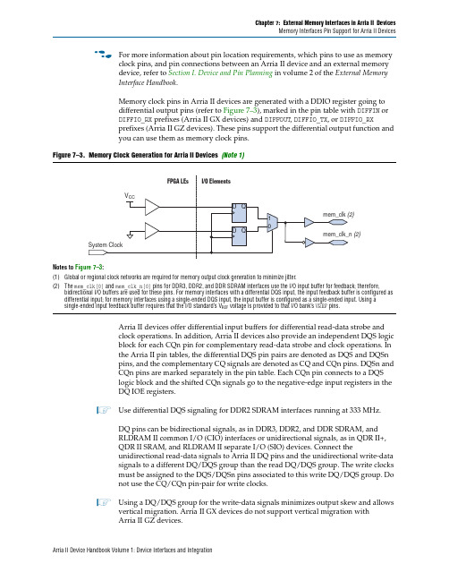
Chapter 7:External Memory Interfaces in Arria II DevicesMemory Interfaces Pin Support for Arria II Devicesf For more information about pin location requirements, which pins to use as memoryclock pins, and pin connections between an Arria II device and an external memorydevice, refer to Section I. Device and Pin Planning in volume 2 of the External MemoryInterface Handbook.Memory clock pins in Arria II devices are generated with a DDIO register going todifferential output pins (refer to Figure7–3), marked in the pin table with DIFFIN orDIFFIO_RX prefixes (Arria II GX devices) and DIFFOUT, DIFFIO_TX, or DIFFIO_RXprefixes (Arria II GZ devices). These pins support the differential output function andyou can use them as memory clock pins.Figure7–3.Memory Clock Generation for Arria II Devices(Note1)Notes to Figure7–3:(1)Global or regional clock networks are required for memory output clock generation to minimize jitter.(2)The mem_clk[0] and mem_clk_n[0] pins for DDR3, DDR2, and DDR SDRAM interfaces use the I/O input buffer for feedback; therefore,bidirectional I/O buffers are used for these pins. For memory interfaces with a differential DQS input, the input feedback buffer is configured as differential input; for memory interfaces using a single-ended DQS input, the input buffer is configured as a single-ended input. Using a single-ended input feedback buffer requires that the I/O standard’s V REF voltage is provided to that I/O bank’s VREF pins.Arria II devices offer differential input buffers for differential read-data strobe andclock operations. In addition, Arria II devices also provide an independent DQS logicblock for each CQn pin for complementary read-data strobe and clock operations. Inthe Arria II pin tables, the differential DQS pin pairs are denoted as DQS and DQSnpins, and the complementary CQ signals are denoted as CQ and CQn pins. DQSn andCQn pins are marked separately in the pin table. Each CQn pin connects to a DQSlogic block and the shifted CQn signals go to the negative-edge input registers in theDQ IOE registers.1Use differential DQS signaling for DDR2 SDRAM interfaces running at 333MHz.DQ pins can be bidirectional signals, as in DDR3, DDR2, and DDR SDRAM, andRLDRAM II common I/O (CIO) interfaces or unidirectional signals, as in QDR II+,QDR II SRAM, and RLDRAM II separate I/O (SIO) devices. Connect theunidirectional read-data signals to Arria II DQ pins and the unidirectional write-datasignals to a different DQ/DQS group than the read DQ/DQS group. The write clocksmust be assigned to the DQS/DQSn pins associated to this write DQ/DQS group. Donot use the CQ/CQn pin-pair for write clocks.1Using a DQ/DQS group for the write-data signals minimizes output skew and allows vertical migration. Arria II GX devices do not support vertical migration withArria II GZ devices.Arria II Device Handbook Volume 1: Device Interfaces and IntegrationChapter 6:I/O Features in Arria II DevicesTermination Schemes for I/O Standardsmini-LVDSArria II GX devices support true mini-LVDS with a three-resistor network using twosingle-ended output buffers for external three-resistor networks.For Arria II GZ devices, use two single-ended output buffers with external one- orthree-resistor networks (mini-LVDS_E_1R or mini-LVDS_E_3R). Arria II GZ row I/Obanks support mini-LVDS output using true LVDS output buffers without an externalresistor network.Figure6–18 shows the one-resistor and three-resistor topology for RSDS andmini-LVDS I/O standard termination.Figure6–18.RSDS and mini-LVDS I/O Standard Termination for Arria II Devices(Note1)Notes to Figure6–18:(1)R p = 170 Ω and R s= 120 Ω(2)mini-LVDS_E_1R is applicable for Arria II GZ devices only.A resistor network is required to attenuate the LVDS output-voltage swing to meetRSDS and mini-LVDS specifications. You can modify the three-resistor networkvalues to reduce power or improve the noise margin. The resistor values chosenshould satisfy the equation shown in Equation6–1.Equation6–1.Resistor Network1To validate that custom resistor values meet the RSDS requirements, Alterarecommends performing additional simulations with IBIS models.f For more information about the RSDS I/O standard, refer to the RSDS Specificationfrom the National Semiconductor website at .f For more information about the mini-LVDS I/O standard, see the mini-LVDSSpecification from the Texas Instruments website at .Arria II Device Handbook Volume 1: Device Interfaces and IntegrationChapter 6:I/O Features in Arria II DevicesArria II OCT CalibrationArria II OCT CalibrationArria II GX devices support calibrated R S OCT and Arria II GZ devices supportcalibrated R S and R T OCT on all I/O pins. You can calibrate the I/O banks with any ofthe OCT calibration blocks available in the device provided the V CCIO of the I/O bankwith the pins using calibrated OCT matches the V CCIO of the I/O bank with thecalibration block and its associated RUP and RDN pins.f For more information about the location of the OCT calibration blocks in Arria IIdevices, refer to the Arria II Device Family Connection Guidelines and Arria II DevicePin-Outs.OCT Calibration BlockAn OCT calibration block has the same V CCIO as the I/O bank that contains the block.R S OCT calibration is supported on all user I/O banks with different V CCIO voltagestandards, up to the number of available OCT calibration blocks. You can configureI/O banks to receive calibrated codes from any OCT calibration block with the sameV CCIO. All I/O banks with the same V CCIO can share one OCT calibration block, even ifthat particular I/O bank has an OCT calibration block.For example, Figure6–10 shows a group of I/O banks that has the same V CCIOvoltage. If a group of I/O banks has the same V CCIO voltage, you can use one OCTcalibration block to calibrate the group of I/O banks placed around the periphery.Because banks 3B, 4C, 6C, and 7B have the same V CCIO as bank 7A, you can calibrateall four I/O banks (3B, 4C, 6C, and 7B) with the OCT calibration block (CB7) locatedin bank 7A. You can enable this by serially shifting out R S OCT calibration codes fromthe OCT calibration block located in bank 7A to the I/O banks located around theperiphery.1I/O banks that do not contain calibration blocks share calibration blocks with I/O banks that do contain calibration blocks.Arria II Device Handbook Volume 1: Device Interfaces and Integration。
MB90F546GSPF中文资料

2
MB90540/540G/545/545G Series
(Continued) • UART 1 With full-duplex double buffer (8-bit length) Clock asynchronized or clock synchronized serial (extended I/O serial) can be used. • External interrupt circuit (8 channels) A module for starting an extended intelligent I/O service (EI2OS) and generating an external interrupt which is triggered by an external input. • Delayed interrupt generation module Generates an interrupt request for switching tasks. • 8/10-bit A/D converter (8 channels) 8/10-bit resolution can be selectively used. Starting by an external trigger input. Conversion time : 26.3 µs • FULL-CAN interfaces MB90540 series : 2 channel MB90545 series : 1 channel Conforming to Version 2.0 Part A and Part B Flexible message buffering (mailbox and FIFO buffering can be mixed) • External bus interface : Maximum address space 16 Mbytes • Package: QFP-100, LQFP-100
ADF4158_cn

ADF4158
特性
RF带宽达6.1 GHz 25位固定模数可提供次赫兹频率分辨率 频率与相位调制能力 频域中的锯齿波和三角波 抛物线斜坡 斜坡与FSK叠加 具有2种不同扫描速率的斜坡 斜坡延迟 斜坡频率回读 斜坡中断 2.7 V至3.3 V电源供电 独立的电荷泵电源VP可提供扩展的调谐电压 可编程电荷泵电流 三线式串行接口 数字锁定检测 关断模式 减少周跳以缩短锁定时间 在宽带宽内快速锁定模式 通过汽车应用认证
概述
ADF4158是一款具有调制和波形产生能力的6.1 GHz小数N分 频频率合成器,包含25位固定模数,可在6.1 GHz下提供次 赫兹频率分辨率。它由低噪声数字鉴频鉴相器 (PFD)、精 密电荷泵和可编程参考分频器组成。该器件内置一个 Σ-Δ 型小数插值器,能够实现可编程模数小数 N分频。 INT和 FRAC寄存器可构成一个总N分频器(N = INT + (FRAC/225))。 ADF4158 可用于实现频移键控 (FSK) 和相移键控 (PSK) 调 制。可用的频率扫描模式也有很多,可在频域内产生各种 波形,例如锯齿波和三角波。 ADF4158 具有周跳减少电 路,可进一步缩短锁定时间,而无需修改环路滤波器。 所有片内寄存器均通过简单的三线式接口进行控制。该器 件采用2.7 V至3.3 V电源供电,不用时可以关断。
ADI中文版数据手册是英文版数据手册的译文,敬请谅解翻译中可能存在的语言组织或翻译错误,ADI不对翻译中存在的差异或由此产生的错误负责。如需确认任何词语的准确性,请参考ADI提供 的最新英文版数据手册。
08728-001
ADF4158 目录
特性 ...............................................
ATM8F8040 数据手册说明书
第1共13页页ATM8F8040数据手册版本号更新时间更新内容V1.02020-09-05V1.0正式版本发布V1.12020-09-16V1.1版本发布,修正DNL参数V1.22020-12-10统一数据手册和应用手册的关于T2CAP的描述V1.32021-3-1增加16脚SOP16封装信息V1.42021-3-8更新IDD2测试条件第2页1.主要特色CPU 特性通信8位1T 8051内核支持两路UART 支持1/2/4/8系统分频模拟模块支持双DPTR 支持12路12位ADC 支持双线调试支持上电复位ROM支持低压复位16K 字节FLASH(擦写寿命1000次)时钟128字节EEPROM(擦写寿命10000次)内部时钟频率最高到32MHz,1%精度数据保持时间:10年内部时钟32KHz 低频振荡器RAM支持外部1-20MHz 晶振256字节内部IRAM 工作模式512字节外部XRAM 正常模式GPIO待机模式(IDLE)最多支持18个GPIO 停机模式(Stop),最小电流<1uA 支持任意端口变化中断工作条件Timer/PWM工作频率:最大32MHz 16位8051标准定时器T0/T1工作电压: 2.7~5.5V 带捕获和可编程输出的16位定时器T2工作温度:-40℃~85℃7路16位带互补输出PWM 输出模块封装唤醒Timer 20-TSSOP 看门狗定时器20-QFN 4x4SOP16其他CRC16循环冗余检测模块可配置逻辑计算单元(CPL)外部晶振停振检测1.主要特色 (2)2.概述 (4)2.1.说明 (4)2.2.应用方向 (4)3.设计框图 (4)4.引脚分布图 (5)5.封装尺寸图 (7)5.1.20-TSSOP (7)5.2.20-QFN (8)5.3.SOP16 (9)6.电气特性 (10)6.1.极限参数 (10)6.2.DC特性 (10)6.3.ADC特性 (11)6.4.内部高频振荡器特性 (11)6.5.内部低频振荡器特性 (11)6.6.外部振荡器特性 (12)6.7.存储器工作特性 (12)6.8.外部复位及中断管脚特性 (12)7.芯片选型 (13)2.概述2.1.说明ATM8F8040是一款内嵌16K字节FLASH的8位单片机。
Artisan Technology Group 产品说明说明书

Calibration Services OverviewWith National Instruments Calibration Services,you can have confidence in your measurements andkeep your measurement devices operating in peakprecision.NI recommends that you externallycalibrate most of your measurement hardwareannually,or at intervals recommended in theproduct’s specification.What Is Calibration?Calibration determines the error associated witha measurement,and,if possible,reduces that error.This means that calibration is more than just adjusting themeasurement capability of a device.Instead,the calibrationprocess includes three parts:•Verifying that the measurement capability of the measurement device is within specification•Adjusting the device to reduce its measurement error •Verifying the new measurement capability of the deviceto ensure that it is operating within specificationsInternational committees have created calibration guidelines to ensure procedural consistency and calibration acceptance among companies and countries.Benefits of CalibrationCalibration improves your measurement accuracy and ensures that your product meets its required specifications.Calibration also provides a number of other benefits,such as:•Increased production yields•Overall measurement consistency•Standardization of qualityTo maintain your measurement accuracy,you must calibrate your measurement device at set intervals.External Calibration and Self-CalibrationY ou can externally calibrate all National Instruments measurement products and self-calibrate many of them.With external calibration, you can ensure that measurement accuracy is traceable to a known standard.External calibration requires the use of high-precision calibration standards.Metrology laboratories or other facilities maintain traceable standards for this type of calibration.Through self-calibration,you adjust the measurement device for use in environments other than those in which it was externally calibrated. In essence,self-calibration acts as the autocalibration or autozero found on benchtop instruments.System CalibrationEven if all of your measurement components are properly calibrated, your system still can have uncertainties associated with cabling and transducers.You can reduce these uncertainties by performing a system calibration.Also known as end-to-end calibration,system calibration is a software compensation method to remove system errors from measurements.By applying a known source to the input of your measurement system and taking readings,you can quickly determine the correction factor to apply to future measurements. System calibration does not replace the need to externally calibrate each component of your system according to the recommended calibration time interval of each component.You can perform a system calibration on any computer-based system you have. For more information on how to perform a system calibration, visit /calibration.Calibration CertificatesNational Instruments ships all hardware products with a Certificate of Conformance.This certificate states that the product has been tested and meets all of its performance standards.In addition,for many products NI provides an online Basic Calibration Certificate. The Basic Calibration Certificate provides NIST-traceable documentation and states that the calibration process conforms to relevant ISO 9002 clauses.You can view your Basic Calibration Certificate at /calibration.If you need a higher level of certification or detailed calibration data,NI can supply ANSI/NCSL Z540-1-compliant certificates for selected products.Calibration Services2National Instruments •Tel: (800) 813 3693•***********•National Instruments and Calibration ServicesNI offers two levels of calibration services – Basic Calibration Service and Detailed Calibration Service.Both are traceable to national and international standards.For situations requiring ANSI Z540compliance,or detailed calibration data,you can purchase Detailed Calibration Service.Simply return your measurement device to National Instruments and order the service as needed or on a regularly scheduled basis.Basic Calibration ServiceDepending on your calibration requirements,you can return your measurement product for basic,traceable recalibration.NI provides an online Basic Calibration Certificate stating that the calibration process conforms to relevant ISO 9002 clauses.Detailed Calibration ServiceInternational committees have created calibration guidelines,such as ANSI/NCSL Z540-1,to ensure acceptable calibration verification and adjustment between companies and countries.For situations requiring ANSI Z540 compliance or detailed calibration data,you can purchase Detailed Calibration service.Manual Calibration ProceduresFor metrology laboratories and companies that maintain calibration facilities,NI offers manual calibration procedures for selected products.These procedures eliminate the need to send your product to National Instruments or a metrology laboratory for calibration.However,to use these procedures,you must have a good working knowledge of metrology and access to traceable calibration standards.You can access NI manual calibration procedures at /calibration .Automated CalibrationManual calibration can be time-consuming and costly.The National Instruments Calibration Executive,developed primarily for metrology laboratories,automates the verification and adjustment of your NI products.By using NI Calibration Executive,you easily can automate your calibration operations and benefit from NI technology such as National Instruments LabVIEW,NI-VISA,Interchangeable Virtual Instruments (IVI),andNational Instruments TestStand.Figure 1. To view your basic certificate, visit /calibration .3National Instruments •Tel: (800) 813 3693•***********•Calibration ServicesNI Calibration ExecutiveNational Instruments Calibration Executive provides an integrated software environment for verifying andadjusting NI measurement devices.Calibration Executive is designed using NI LabVIEW,NI-VISA,IVI,and NI TestStand.Additional HardwareCalibration Executive includes all of the software you need for calibrating your NI measurement device.In addition to your calibration instruments,you also need hardware such as adapters,cables,and chassis.Order the appropriate calibration-specific hardware for your measurement device.For a complete list of required NI hardware and recommended calibration instruments,visit /calibration .Contacting NI for Calibration ServicesTo return your product to NI for calibration services,please contact us to obtain pricing,terms of service,and a return material authorization (RMA) for recalibration.If you require calibration services in your local area,NI also offers calibration through metrology laboratories in selected countries.Visit /calibration for a list of applicable products and calibration service providers in your local area.Calibration ServicesBasic Certificate of CalibrationDetailed Certificate of Calibration forhigh-speed digitizers,DSA,DMMs,signal generators,loggers,or analog output products E Series,M Series,and S Series devices SCXI products NI FieldPoint Calibration Executive SoftwareNI Calibration Executive..............................................777608-02Calibration-Specific HardwareCalibration Executive hardware adapterfor E Series,M Series,and S Series devices ............778056-03Calibration Executive hardware adapterfor NI 435x devices ..................................................778031-03FieldPoint FP-TB-CAL calibration base......................777519-90BUY NOW!For complete product specifications,pricing,andaccessory information,call (800) 813 3693 (U.S.only) or go to /calibration .Ordering Information© 2005 National Instruments Corporation. All rights reserved. FieldPoint, LabVIEW, National Instruments, National Instruments Alliance Partner, NI, ,NI TestStand, NI-VISA, and SCXI are trademarks of National Instruments. Other product and company names listed are trademarks or trade names of their respective NI Services and Supportand development through deployment and ongoing maintenance.We offer services and service levels to meet customer requirements in research,design,validation,Visit /services .Training and CertificationNI training is the fastest,most certain route to productivity with our products.NI training can shorten your learning curve,save development time,and reduce maintenance costs over the application life cycle.We schedule instructor-led courses in cities worldwide,or we can hold a course at your facility.We also offer a professional certification program that identifies individuals who have high levels of skill and knowledge on using NI products.Visit /training .Professional ServicesOur Professional Services Team is comprised of NI applications engineers,NI Consulting Services,and a worldwide National Instruments Alliance Partner program of more than 600 independent consultantsand integrators.Services range from start-up assistance to turnkey system integration.Visit /alliance .OEM SupportWe offer design-in consulting and product integration assistance if you want to use our products for OEM applications.For information about special pricing and services for OEM customers,visit /oem .Local Sales and Technical SupportIn offices worldwide,our staff is local to the country,giving you access to engineers who speak your language.NI delivers industry-leading technical support through online knowledge bases,our applications engineers,and access to 14,000 measurement and automation professionals within NI Developer Exchange forums.Find immediate answers to your questions at /support .We also offer service programs that provide automatic upgrades to your application development environment and higher levels of technical support.Visit /ssp .Hardware ServicesNI Factory Installation ServicesNI Factory Installation Services (FIS) is the fastest and easiest way to use your PXI or PXI/SCXI combination systems right out of the box.Trained NI technicians install the software and hardware and configure the system to your specifications.NI extends the standard warranty by one year on hardware components (controllers,chassis,modules) purchased with FIS.To use FIS,simply configure your system online with /pxiadvisor .Calibration ServicesNI recognizes the need to maintain properly calibrated devices for high-accuracy measurements.We provide manual calibration procedures,services to recalibrate your products,and automated calibration software specifically designed for use by metrology laboratories.Visit /calibration .Repair and Extended WarrantyNI provides complete repair services for our products.Express repairand advance replacement services are also available.We offer extended warranties to help you meet project life-cycle requirements.Visit /services .National Instruments • *********** • (800) 813 36932005_5630_812_101_D。
c8051f340定时器八位重装使用程序附头文件

// Pinout://// P2.2 -> LED#include <C8051F340.h> // SFR declarations show at the end of the file#define SYSCLK 12000000/8 // SYSCLK in Hz (12 MHz internal// oscillator / 8)// the internal oscillator has a// tolerance of +/- 2%#define TIMER_PRESCALER 48 // Based on Timer CKCON settings// There are SYSCLK/TIMER_PRESCALER timer ticks per second, so// SYSCLK/TIMER_PRESCALER/1000 timer ticks per millisecond.#define TIMER_TICKS_PER_MS SYSCLK/TIMER_PRESCALER/1000// Note: TIMER_TICKS_PER_MS should not exceed 255 (0xFF) for the 8-bit timer#define AUX1 TIMER_TICKS_PER_MS#define AUX2 -AUX1#define LED_TOGGLE_RATE 100 // LED toggle rate in milliseconds// if LED_TOGGLE_RATE = 1, the LED will// be on for 1 millisecond and off for// 1 millisecond#define TIMER0_RELOAD_HIGH AUX2 // Reload value for Timer0 high bytesbit LED = P2^2; // LED//-----------------------------------------------------------------------------// Function Prototypes//-----------------------------------------------------------------------------void Port_Init (void); // Port initialization routinevoid Timer0_Init (void); // Timer0 initialization routine//-----------------------------------------------------------------------------// main() Routine//-----------------------------------------------------------------------------void main (void){PCA0MD &= ~0x40; // WDTE = 0 (clear watchdog timer// enable)Timer0_Init (); // Initialize the Timer0Port_Init (); // Init PortsEA = 1; // Enable global interruptswhile (1); // Loop forever}//-----------------------------------------------------------------------------// Initialization Subroutines//-----------------------------------------------------------------------------//-----------------------------------------------------------------------------// Port_Init//-----------------------------------------------------------------------------//// Return Value : None// Parameters : None//// This function configures the crossbar and GPIO ports.//// Pinout://// P2.2 -> LED//// all other port pins unused////-----------------------------------------------------------------------------void Port_Init (void){XBR1 = 0x40; // Enable crossbarP2MDOUT = 0x0C; // Set LEDs}//-----------------------------------------------------------------------------// Timer0_Initvoid Timer0_Init(void){TH0 = TIMER0_RELOAD_HIGH; // Init Timer0 High registerTL0 = TH0; // Set the intial Timer0 valueTMOD = 0x02; // Timer0 in 8-bit reload modeCKCON = 0x02; // Timer0 uses a 1:48 prescaler ET0=1; // Timer0 interrupt enabled TCON = 0x10; // Timer0 ON}//-----------------------------------------------------------------------------// Interrupt Service Routines//-----------------------------------------------------------------------------//-----------------------------------------------------------------------------// Timer0_ISR//-----------------------------------------------------------------------------//// Here we process the Timer0 interrupt and toggle the LED when appropriate ////-----------------------------------------------------------------------------void Timer0_ISR (void) interrupt 1{static int counter = 0;if((counter++) == LED_TOGGLE_RATE){LED = ~LED; // Toggle the LEDcounter = 0;}}//-----------------------------------------------------------------------------// End Of File//-----------------------------------------------------------------------------//C8051f340.h//-----------------------------------------------------------------------------#ifndef C8051F340_H#define C8051F340_H//-----------------------------------------------------------------------------// Byte Registers//-----------------------------------------------------------------------------sfr P0 = 0x80; // Port 0 Latchsfr SP = 0x81; // Stack Pointersfr DPL = 0x82; // Data Pointer Lowsfr DPH = 0x83; // Data Pointer Highsfr EMI0TC = 0x84; // EMIF Timingsfr EMI0CF = 0x85; // EMIF Configurationsfr OSCLCN = 0x86; // Internal Low-Freq Oscillator Control sfr PCON = 0x87; // Power Controlsfr TCON = 0x88; // Timer/Counter Controlsfr TMOD = 0x89; // Timer/Counter Modesfr TL0 = 0x8A; // Timer/Counter 0 Lowsfr TL1 = 0x8B; // Timer/Counter 1 Lowsfr TH0 = 0x8C; // Timer/Counter 0 Highsfr TH1 = 0x8D; // Timer/Counter 1 Highsfr CKCON = 0x8E; // Clock Controlsfr PSCTL = 0x8F; // Program Store R/W Controlsfr P1 = 0x90; // Port 1 Latchsfr TMR3CN = 0x91; // Timer/Counter 3Controlsfr TMR3RLL = 0x92; // Timer/Counter 3 Reload Lowsfr TMR3RLH = 0x93; // Timer/Counter 3 Reload Highsfr TMR3L = 0x94; // Timer/Counter 3Lowsfr TMR3H = 0x95; // Timer/Counter 3 Highsfr USB0ADR = 0x96; // USB0 Indirect Address Registersfr USB0DAT = 0x97; // USB0 Data Registersfr SCON0 = 0x98; // UART0 Controlsfr SBUF0 = 0x99; // UART0 Data Buffersfr CPT1CN = 0x9A; // Comparator1 Controlsfr CPT0CN = 0x9B; // Comparator0 Controlsfr CPT1MD = 0x9C; // Comparator1 Mode Selectionsfr CPT0MD = 0x9D; // Comparator0 Mode Selectionsfr CPT1MX = 0x9E; // Comparator1 MUX Selectionsfr CPT0MX = 0x9F; // Comparator0 MUX Selectionsfr P2 = 0xA0; // Port 2 Latchsfr SPI0CFG = 0xA1; // SPI Configurationsfr SPI0CKR = 0xA2; // SPI Clock Rate Controlsfr SPI0DAT = 0xA3; // SPI Datasfr P0MDOUT = 0xA4; // Port 0 Output Mode Configuration sfr P1MDOUT = 0xA5; // Port 1 Output Mode Configuration sfr P2MDOUT = 0xA6; // Port 2 Output Mode Configuration sfr P3MDOUT = 0xA7; // Port 3 Output Mode Configuration sfr IE = 0xA8; // Interrupt Enablesfr CLKSEL = 0xA9; // Clock Selectsfr EMI0CN = 0xAA; // External Memory Interface Control sfr SBCON1 = 0xAC; // UART1 Baud Rate Generator Control sfr P4MDOUT = 0xAE; // Port 4 Output Mode Configuration sfr PFE0CN = 0xAF; // Prefetch Engine Controlsfr OSCXCN = 0xB1; // External Oscillator Controlsfr OSCICN = 0xB2; // Internal Oscillator Controlsfr OSCICL = 0xB3; // Internal Oscillator Calibrationsfr SBRLL1 = 0xB4; // UART1 Baud Rate Generator Lowsfr SBRLH1 = 0xB5; // UART1 Baud Rate Generator High sfr FLSCL = 0xB6; // Flash Scalesfr FLKEY = 0xB7; // Flash Lock and Keysfr IP = 0xB8; // Interrupt Prioritysfr CLKMUL = 0xB9; // Clock Multipliersfr AMX0N = 0xBA; // AMUX0 Negative Channel Select sfr AMX0P = 0xBB; // AMUX0 Positive Channel Selectsfr ADC0CF = 0xBC; // ADC0 Configurationsfr ADC0L = 0xBD; // ADC0 Lowsfr ADC0H = 0xBE; // ADC0 Highsfr SMB0CN = 0xC0; // SMBus Controlsfr SMB0CF = 0xC1; // SMBus Configurationsfr SMB0DAT = 0xC2; // SMBus Datasfr ADC0GTL = 0xC3; // ADC0 Greater-Than Compare Low sfr ADC0GTH = 0xC4; // ADC0 Greater-Than Compare High sfr ADC0LTL = 0xC5; // ADC0 Less-Than Compare Word Low sfr ADC0LTH = 0xC6; // ADC0 Less-Than Compare Word High sfr P4 = 0xC7; // Port 4 Latchsfr TMR2CN = 0xC8; // Timer/Counter 2 Controlsfr REG0CN = 0xC9; // Voltage Regulator Controlsfr TMR2RLL = 0xCA; // Timer/Counter 2 Reload Lowsfr TMR2RLH = 0xCB; // Timer/Counter 2 Reload Highsfr TMR2L = 0xCC; // Timer/Counter 2 Lowsfr TMR2H = 0xCD; // Timer/Counter 2 Highsfr PSW = 0xD0; // Program Status Wordsfr REF0CN = 0xD1; // Voltage Reference Controlsfr SCON1 = 0xD2; // UART1 Controlsfr SBUF1 = 0xD3; // UART1 Data Buffersfr P0SKIP = 0xD4; // Port 0 Skipsfr P1SKIP = 0xD5; // Port 1 Skipsfr P2SKIP = 0xD6; // Port 2 Skipsfr USB0XCN = 0xD7; // USB0 Transceiver Controlsfr PCA0CN = 0xD8; // PCA0 Controlsfr PCA0MD = 0xD9; // PCA0 Modesfr PCA0CPM0 = 0xDA; // PCA0 Module 0 Mode Registersfr PCA0CPM1 = 0xDB; // PCA0 Module 1 Mode Registersfr PCA0CPM2 = 0xDC; // PCA0 Module 2 Mode Registersfr PCA0CPM3 = 0xDD; // PCA0 Module 3 Mode Registersfr PCA0CPM4 = 0xDE; // PCA0 Module 4 Mode Registersfr ACC = 0xE0; // Accumulatorsfr XBR0 = 0xE1; // Port I/O Crossbar Control 0sfr XBR1 = 0xE2; // Port I/O Crossbar Control 1sfr XBR2 = 0xE3; // Port I/O Crossbar Control 2sfr IT01CF = 0xE4; // INT0/INT1 Configurationsfr SMOD1 = 0xE5; // UART1 Modesfr EIE1 = 0xE6; // Extended Interrupt Enable 1sfr EIE2 = 0xE7; // Extended Interrupt Enable 2sfr ADC0CN = 0xE8; // ADC0 Controlsfr PCA0CPL1 = 0xE9; // PCA0 Capture 1 Lowsfr PCA0CPH1 = 0xEA; // PCA0 Capture 1 Highsfr PCA0CPL2 = 0xEB; // PCA0 Capture 2 Lowsfr PCA0CPH2 = 0xEC; // PCA0 Capture 2 Highsfr PCA0CPL3 = 0xED; // PCA0 Capture 3 Lowsfr PCA0CPH3 = 0xEE; // PCA0 Capture 3 Highsfr RSTSRC = 0xEF; // Reset Source Configuration/Status sfr B = 0xF0; // B Registersfr P0MDIN = 0xF1; // Port 0 Input Mode Configuration sfr P1MDIN = 0xF2; // Port 1 Input Mode Configuration sfr P2MDIN = 0xF3; // Port 2 Input Mode Configuration sfr P3MDIN = 0xF4; // Port 3 Input Mode Configuration sfr P4MDIN = 0xF5; // Port 4 Input Mode Configuration sfr EIP1 = 0xF6; // Extended Interrupt Priority 1sfr EIP2 = 0xF7; // Extended Interrupt Priority 2sfr SPI0CN = 0xF8; // SPI0 Controlsfr PCA0L = 0xF9; // PCA0 Counter Lowsfr PCA0H = 0xFA; // PCA0 Counter Highsfr PCA0CPL0 = 0xFB; // PCA0 Capture 0 Lowsfr PCA0CPH0 = 0xFC; // PCA0 Capture 0 Highsfr PCA0CPL4 = 0xFD; // PCA0 Capture 4 Lowsfr PCA0CPH4 = 0xFE; // PCA0 Capture 4 Highsfr VDM0CN = 0xFF; // VDD Monitor Control//-----------------------------------------------------------------------------// Bit Definitions//-----------------------------------------------------------------------------// TCON 0x88sbit TF1 = 0x8F; // Timer1 overflow flagsbit TR1 = 0x8E; // Timer1 on/off controlsbit TF0 = 0x8D; // Timer0 overflow flagsbit TR0 = 0x8C; // Timer0 on/off controlsbit IE1 = 0x8B; // Ext interrupt 1 edge flagsbit IT1 = 0x8A; // Ext interrupt 1 typesbit IE0 = 0x89; // Ext interrupt 0 edge flagsbit IT0 = 0x88; // Ext interrupt 0 type// SCON0 0x98sbit S0MODE = 0x9F; // Serial mode control bit 0// Bit6 UNUSEDsbit MCE0 = 0x9D; // Multiprocessor communication enable sbit REN0 = 0x9C; // Receive enablesbit TB80 = 0x9B; // Transmit bit 8sbit RB80 = 0x9A; // Receive bit 8sbit TI0 = 0x99; // Transmit interrupt flagsbit RI0 = 0x98; // Receive interrupt flag// IE 0xA8sbit EA = 0xAF; // Global interrupt enablesbit ESPI0 = 0xAE; // SPI0 interrupt enablesbit ET2 = 0xAD; // Timer2 interrupt enablesbit ES0 = 0xAC; // UART0 interrupt enablesbit ET1 = 0xAB; // Timer1 interrupt enablesbit EX1 = 0xAA; // External interrupt 1 enablesbit ET0 = 0xA9; // Timer0 interrupt enablesbit EX0 = 0xA8; // External interrupt 0 enable// IP 0xB8// Bit7 UNUSEDsbit PSPI0 = 0xBE; // SPI0 interrupt prioritysbit PT2 = 0xBD; // Timer2 prioritysbit PS0 = 0xBC; // UART0 prioritysbit PT1 = 0xBB; // Timer1 prioritysbit PX1 = 0xBA; // External interrupt 1 prioritysbit PT0 = 0xB9; // Timer0 prioritysbit PX0 = 0xB8; // External interrupt 0 priority// SMB0CN 0xC0sbit MASTER = 0xC7; // Master/slave indicatorsbit TXMODE = 0xC6; // Transmit mode indicatorsbit STA = 0xC5; // Start flagsbit STO = 0xC4; // Stop flagsbit ACKRQ = 0xC3; // Acknowledge requestsbit ARBLOST = 0xC2; // Arbitration lost indicatorsbit ACK = 0xC1; // Acknowledge flagsbit SI = 0xC0; // SMBus interrupt flag// TMR2CN 0xC8sbit TF2H = 0xCF; // Timer2 high byte overflow flagsbit TF2L = 0xCE; // Timer2 low byte overflow flagsbit TF2LEN = 0xCD; // Timer2 low byte interrupt enablesbit T2SOF = 0xCC; // Timer2 start-of-frame capture enable sbit T2SPLIT = 0xCB; // Timer2 split mode enablesbit TR2 = 0xCA; // Timer2 on/off control// Bit1 UNUSEDsbit T2XCLK = 0xC8; // Timer2 external clock select// PSW 0xD0sbit CY = 0xD7; // Carry flagsbit AC = 0xD6; // Auxiliary carry flagsbit F0 = 0xD5; // User flag 0sbit RS1 = 0xD4; // Register bank select 1sbit RS0 = 0xD3; // Register bank select 0sbit OV = 0xD2; // Overflow flagsbit F1 = 0xD1; // User flag 1sbit P = 0xD0; // Accumulator parity flag// PCA0CN 0xD8sbit CF = 0xDF; // PCA0 counter overflow flagsbit CR = 0xDE; // PCA0 counter run control// Bit5 UNUSEDsbit CCF4 = 0xDC; // PCA0 module4 capture/compare flag sbit CCF3 = 0xDB; // PCA0 module3 capture/compare flag sbit CCF2 = 0xDA; // PCA0 module2 capture/compare flag sbit CCF1 = 0xD9; // PCA0 module1 capture/compare flag sbit CCF0 = 0xD8; // PCA0 module0 capture/compare flag// ADC0CN 0xE8sbit AD0EN = 0xEF; // ADC0 enablesbit AD0TM = 0xEE; // ADC0 track modesbit AD0INT = 0xED; // ADC0 converision complete interrupt flag sbit AD0BUSY = 0xEC; // ADC0 busy flagsbit AD0WINT = 0xEB; // ADC0 window compare interrupt flag sbit AD0CM2 = 0xEA; // ADC0 conversion mode select 2sbit AD0CM1 = 0xE9; // ADC0 conversion mode select 1sbit AD0CM0 = 0xE8; // ADC0 conversion mode select 0// SPI0CN 0xF8sbit SPIF = 0xFF; // SPI0 interrupt flagsbit WCOL = 0xFE; // SPI0 write collision flagsbit MODF = 0xFD; // SPI0 mode fault flagsbit RXOVRN = 0xFC; // SPI0 rx overrun flagsbit NSSMD1 = 0xFB; // SPI0 slave select mode 1sbit NSSMD0 = 0xFA; // SPI0 slave select mode 0sbit TXBMT = 0xF9; // SPI0 transmit buffer empty sbit SPIEN = 0xF8; // SPI0 SPI enable//-----------------------------------------------------------------------------// Interrupt Priorities//-----------------------------------------------------------------------------#define INTERRUPT_INT0 0 // External Interrupt 0#define INTERRUPT_TIMER0 1 // Timer0 Overflow#define INTERRUPT_INT1 2 // External Interrupt 1#define INTERRUPT_TIMER1 3 // Timer1 Overflow#define INTERRUPT_UART0 4 // Serial Port 0#define INTERRUPT_TIMER2 5 // Timer2 Overflow#define INTERRUPT_SPI0 6 // Serial Peripheral Interface 0#define INTERRUPT_SMBUS0 7 // SMBus0 Interface#define INTERRUPT_USB0 8 // USB Interface#define INTERRUPT_ADC0_WINDOW 9 // ADC0 Window Comparison #define INTERRUPT_ADC0_EOC 10 // ADC0 End Of Conversion#define INTERRUPT_PCA0 11 // PCA0 Peripheral#define INTERRUPT_COMPARATOR0 12 // Comparator0#define INTERRUPT_COMPARATOR1 13 // Comparator1#define INTERRUPT_TIMER3 14 // Timer3 Overflow#define INTERRUPT_VBUS_LEVEL 15 // VBUS level-triggered interrupt #define INTERRUPT_UART1 16 // Serial Port 1//-----------------------------------------------------------------------------// Header File PreProcessor Directive//-----------------------------------------------------------------------------#endif // #define C8051F340_H//-----------------------------------------------------------------------------// End Of File//-----------------------------------------------------------------------------。
SMT设备的最新发展趋势

表 面 安 装 技 术 ( T)作 为 新 一 SM 代 电子 组 装 技 术 已 经 渗 透 到 各 个 领
域 ,S MT发 展 迅 速 、 应 用 广 泛 , 在
这 适 应 了双 路 贴 装 和 焊 接 的需 要 。
中 , 焊 膏 长 时 间 暴 露 在 开 放 环 境
下 是 引 起 印 刷 缺 陷 的 重 要 原 因 。 而
上 。
( 新 型 的 模 板 印 刷 设 备 正 朝 2) 智 能 化 方 向 发 展 。 新 型 的 M 1 板 P、模 印 刷 设 备 利 用 改 进 的 视 觉 算 法 , 可
压 力 来 充填 焊膏 , 并 提 供 动压 力 , 使 焊 膏 进 入 开 孔 。这 一 P roF w技 lo 术从根本 上消除 _ r影 响 焊 膏 印 刷 的 最 大 变 量 因 素 , 使 用 户 无 需 考 虑 印
这 种 新 型 的 印刷 设 备 在 保 留 印刷 机
主 要 性 能 的基 础 上 , 将 传 统 的输 送 和 印 刷 单 路 结 构 改 为 双 路 结 构 , 可
以 进 行 双 路 PCB的 输 入 、 定 位 、 校
D EK公 司 推 出 的 IroFlo w封 闭 挤 压 式 印 刷 头 可 有 效 解 决 上 述 问 题 。 与 焊膏 在 开放 的环 境 中滚 动 不 同 ,
维普资讯
.: 。 ■ ■ ■ ● ■ ■ ■ ■ .; ■ ● ■ 。 ■ ■ — ■ . 二
质 量 工 程 卷
Qu i ngne r aly E i e ng t i
Mou t ec n lg a e n d v o e uc l n o d p l a o l t n T h o o y h sb e e  ̄ p d q iky a d g t wi e a pi f n i eecr i ci n onc
- 1、下载文档前请自行甄别文档内容的完整性,平台不提供额外的编辑、内容补充、找答案等附加服务。
- 2、"仅部分预览"的文档,不可在线预览部分如存在完整性等问题,可反馈申请退款(可完整预览的文档不适用该条件!)。
- 3、如文档侵犯您的权益,请联系客服反馈,我们会尽快为您处理(人工客服工作时间:9:00-18:30)。
Doc No. 文件編號: FDEQUI-084Revision 版本: 8AI&SMT New Program Input ProcedureAI&SMT新机種导入程序Page 頁碼: Page 1 of 10Doc No. 文件編號: FDEQUI-084Revision 版本: 8AI&SMT New Program Input ProcedureAI&SMT新机種导入程序Page 頁碼: Page 2 of 101.PURPOSE 目的:Provide regulation regarding how to generate new program of AI& SMT and management the program.规范AI& SMT新程序的制作以及程序的管理.2.SCOPE 範圍:This file is applicable for new AI& SMT placement program .适用于所有新导入AI &SMT贴片程序.3.DEFINITIONS 定義:N/A4.REFERENCE DOCUMENT 參考文件:N/A5.RESPONSIBILITY 職責:AI& SMT engineers or technicians are responsible to edit all the programs and run it.AI& SMT 工程師,技朮員負責編輯程序和試產.6.PROCEDURE 程序:6.1 Get the CAD data. gerber file, BOM, component layout and PCB from engineering department.向工程部索取CAD资料.Gerber文件.位置圖,BOM和PCB.6.2 Whether in SIEMENS. FUJI or Universal machine, all SMT/AI placement program is generated by usingfunction of “CAD Import” in each system. All acceptable CAD data should be in ASCII format that can beopened and edited by text editor such as win notepad and word pad.无论在西门子,富士还是在環球机器中,所有SMT/AI贴片程序都经由系统中 CAD import功能来完成.能够被接受的CAD资料必须是能用文本编辑器打开并编辑的ASCII码格式.6.3 In order to fit this function, CAD data source must include at least coordinates for X,Y and orientation ofeach components, and its Reference ID, Besides, each line of the data source must consist of above mentioned fields with valid field-separator that can be identified by machine system. Commonly, valid separator includes comma, period, slash, back-slash, pipe, space, TAB, colon, semi-colon, @, swung dash, number-sign, etc.,and every line of data source should have same format and same sequence for each field.为了满足“CAD Import”这项功能的要求,所有CAD资料来源都必须包含至少有每一个组件的X,Y坐标及角度,它们的Reference number 以及Part Number. 资料来源的每一行都应包含有前面提及的数据块以及适当的可以被机器系统识别的块分隔符。
一般合法的分隔符包括:,. | / \ ~ @ # ; : 以及TAB和空格。
并且所有行都应有相同的格式以及块排列的顺序。
6.4 Following is CAD data example that can be successfully converted by machine system.下边提供能够被机器系统成功转换的CAD样本。
Doc No. 文件編號: FDEQUI-084Revision 版本: 8AI&SMT New Program Input ProcedureAI&SMT新机種导入程序Page 頁碼: Page 3 of 10 ITEM X Y Angle Location1 20.57, -2.290.0 C242 143.76 25.27 90.00 C413 100.84 5.08 0.0 C44…….6.5 Following is BOM example that can be successfully converted by machine system.下边提供能够被机器系统成功转换的BOM样本。
Item P/N Location1-33268R15,16,20,352-22993C98,45,65,3 -77999IC1,3,8,9,……6.6 In case the CAD data source that customer provided does not meet above requirement, it should be properlyedited until can be successfully converted. If customer provides gerber file instead of CAD data, softwareGC-Place will be used to generate CAD data.如果客户提供的CAD数据不能满足要求,应该先编辑直到能被正确转换。
如果客户提供的是Gerber file 而不是CAD数据时,应优先使用专用软件GC-Place来转换出合适的CAD数据。
6.7 Subsequently, we will utilize “PCB Editor” function in FUJI CAM Line Computer/ Universal machine ,orutilize “siplace-pro” in master database sever computer. In the following editing, whatever machine we use, it all comes down to one strategy: settle down parameter of PCB including length, width, height, and zeropoint of PCB, Vision fiducial, sub-PCB offsets. After that, this file is completed that is able to transmit tomachine for fine tune till production.然后利用FUJI CAM computer 或環球机器中“Program Editor”功能来完成贴片程序, 或用 “Siplace-pro”在主数据服务器电脑是完成贴片程序。
在随后步骤中,不论使用何种机器,都终将归结于:设定PCB 长、宽、厚度以及零点与边距,光学基准点的位置,各子板之间的跨度等完成该程序。
此时该文件即是一个完整的贴片文件,可以传送至机器进行调试并生产.6.8 New part data nomenclature for separate SMT machine in generate program progress as following:新的零件外型命名以不同品牌贴片机按以下几点来命名.6.8.1 For standard CHIP component such as 1005,1608,2012,3216 and standard diode, transistor, IC etc., weDoc No. 文件編號: FDEQUI-084Revision 版本: 8AI&SMT New Program Input ProcedureAI&SMT新机種导入程序Page 頁碼: Page 4 of 10 can copy the existed component from part data library. standard component library according to thedescription of components in the BOM or the actual shape dimension we’ve known . Component namedby its part number for GSM’s programs in proper library . all component’s dimension must use mm unit.针对标准CHIP组件(1005,1608,2012,3216,etc.)以及标准二极管三极管以及标准IC的part data的制定,我们根据组件在BOM上Description或实际的外形尺寸来拷贝现有part data标准组件库中的组件。
例如:CHXXYYTT,表示CHIP零件, DODXXYYTT,表示二极管零件, SOTXXYYTT,表示三极管零件,SOICPPPXXYYTT,表示IC零件, SOPPPPXXYYTT,表示SOP零件,BGAPPPXXYYTT,表示BGA零件, QFPPPPXXYYTT,表示QFP零件, PLCPPPXXYYTT,表示PLACC零件,SOJPPPXXYYTT,表示SOJ零件, CONPPPXXYYTT,表示CONNECTION零件﹐GSM程序的零件按其P/N來命名﹐其他的異型零件給一個合適的命名.所有零件尺寸用毫米為單位。
Doc No. 文件編號: FDEQUI-084Revision 版本: 8AI&SMT New Program Input ProcedureAI&SMT 新机種导入程序Page 頁碼:Page 5 of 106.8.2 Additionally, aim at siemens. Take enactment number code to verification shape code for siemensaccording to siemens manual “job guide”, for standard CHIP component such as1005,1608,2012,3216 and standard diode, transistor, IC etc., we can arrange in pairs from shape data library according to the description of components in the BOM or the actual shape dimension we’ve known 。