红外热像仪使用说明——经典案例分享之LED芯片
LED芯片散热检测-福禄克
查看。
图 3B
2 福禄克公司 LED 芯片散热检测
看见您所看不见的 无论您是设计下一代移动设备、按比例缩减客运 车辆还是开发功能更强大、更轻质的全新聚合物, 都要确保获得最佳的热数据。为了进行准确而高 效的研发红外测试,我们推荐使用 Fluke RSE 系 列 RSE300 和 RSE600 在线式红外热像仪。凭借 可测量低至 40mK 数据的热灵敏度和高达 640 x 480 的分辨率,在线式热像仪可将数据传输到您 的 PC,以进行研发和质量保证分析。 若要详细了解这些多功能、高分辨率、高准确度热 像仪如何帮助您更快速地开发更出色的产品, 请咨询您的福禄克销售代表或访问 /infrared 了解更多信息。
在研发过程中检查 LED 散热片 时,可以使用红外热像仪。热像仪 的读数可以帮助制造商发现材料 和设计方面的潜在问题,以更好地 分析和改善散热片质量。
LED 芯片的温度与散热片的 关系
要持续正常工作,LED 芯片的温度 不得超过 120 °C。芯片随着温度 的升高,使用寿命会缩短。因此, 如果芯片温度非常高,甚至超过 120 °C,芯片的使用寿命将缩短。
因此,为保持芯片性能和使用寿 命,保持在 120 °C 以下非常重要。 这凸显了散热片的重要性,散热片 是用于冷却 LED 芯片的部件。如 果没有散热片、散热片设计不合理 或材料不合适,散热效果将受到严 重影响,从而缩短 LED 的使用寿 命或导致 LED 颜色发生变化。
在引入红外热像仪之前,在 LED 芯片散热研发过程中用什 么来测量温度?
在引入红外热像仪之前,热电偶是 在散热过程中测量温度最常用的 方法。
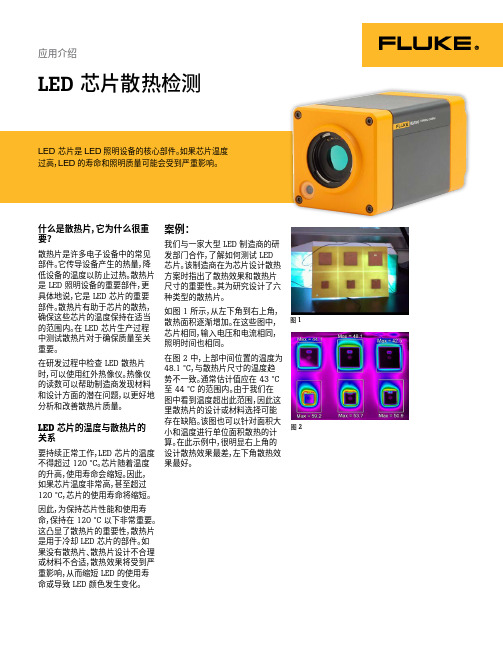
在图 3A 中,LED 芯片(圆形部 分)使用条状散热片,使用 Fluke SmartView® 桌面报告和分析软件 图 4A 对不同距离处的温度分布进行线 性分析,如图 3B 所示。
红外热成像仪高端应用——微米级电子器件检测
红外热成像仪高端应用——微米级电子器件检测随着红外技术的不断发展,红外热像仪逐渐被应用于越来越多的民生行业,吃、穿、住、行无所不在。
美国福禄克热像仪作为行业佼佼者,通过多年的推广和开发,已获得各领域工程师的广泛认可,此文将通过真实案例和热图的解说来阐述美国福禄克热像仪是如何助力微米级电子器件检测的。
微米级小目标通常是温度检测的难点,接触式温度计由于其传感器尺寸限制,对于1mm 以下的目标是无法检测的,高端红外热像仪配套专用的微距镜头, 可对最小32微米的目标进行有效检测,本文以案例叙述使用福禄克大师之选系列热像仪对微米级芯片进行温度检测的过程和系统解决方案。
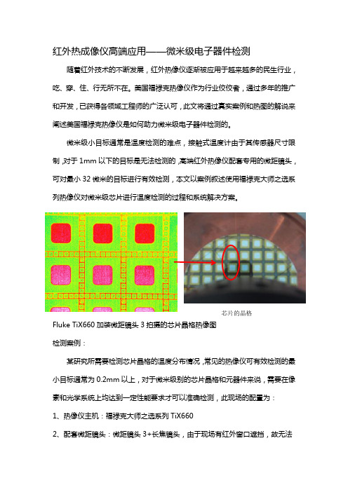
Fluke TiX660加装微距镜头3拍摄的芯片晶格热像图检测案例:某研究所需要检测芯片晶格的温度分布情况,常见的热像仪可有效检测的最小目标通常为0.2mm 以上,对于微米级别的芯片晶格和元器件来说,需要在像素和光学系统上均达到一定性能要求才可以准确检测,此现场的配置为:1、热像仪主机:福禄克大师之选系列TiX6602、配套微距镜头:微距镜头3+长焦镜头,由于现场有红外窗口遮挡,故无法 芯片的晶格近距离检测,需要在10厘米处才可以安放热像仪,微距镜头3+长焦镜头的配置正好可以满足检测小目标和较远的对焦距离的双重需求(微距镜头2必须在2-4厘米处才可有效检测小目标)。
3、为使现场检测对焦方便,使用三脚架+二维可调精密位移云台。
从现场的检测情况来看,两排晶格器件,上排器件的温度为34.1℃,而下排器件的温度为34.2℃,说明在散热方面,各方位排列的器件的散热情况是不相同的,研究人员可以据此测试不同的排列对器件的影响,并对某些问题器件进行单独检测。
大师之选系列热像仪的最小检测目标为32微米,可以充分满足研究人员对微米级小目标的检测需求。
福禄克大师之选系列共配置了三种微距镜头,因检测距离近,故微距镜头不适合用激光自动对焦和自动对焦;若使用手动对焦,需要非常精准的光学系统的调整,而手动对焦在微距检测时容易造成对焦过近或过远,影响检测效果。
红外LED产品说明书.pdf_1718588846.4382489

Dimensions: [mm]Scale - 7:115414194BA21015414194BA21015414194BA21015414194BA21015414194BA210T e m p e r a t u r eT pT L15414194BA210Cautions and Warnings:The following conditions apply to all goods within the product series of Optoelectronic Components of Würth Elektronik eiSos GmbH & Co. KG:General:•This optoelectronic component is designed and manufactured for use in general electronic equipment.•Würth Elektronik must be asked for written approval (following the PPAP procedure) before incorporating the components into any equipment in fields such as military, aerospace, aviation, nuclear control, submarine, transportation (automotive control, train control, ship control), transportation signal, disaster prevention, medical, public information network, etc. where higher safety and reliability are especially required and/or if there is the possibility of direct damage or human injury.•Optoelectronic components that will be used in safety-critical or high-reliability applications, should be pre-evaluated by the customer.•The optoelectronic component is designed and manufactured to be used within the datasheet specified values. If the usage and operation conditions specified in the datasheet are not met, the wire insulation may be damaged or dissolved.•Do not drop or impact the components, the component may be damaged•Würth Elektronik products are qualified according to international standards, which are listed in each product reliability report. Würth Elektronik does not warrant any customer qualified product characteristics beyond Würth Elektroniks’ specifications, for its validity and sustainability over time.•The responsibility for the applicability of the customer specific products and use in a particular customer design is always within the authority of the customer. All technical specifications for standard products also apply to customer specific products.•Unless Würth Elektroik has given its express consent, the customer is under no circumstances entitled to reverse engineer, disassemble or otherwise attempt to extract knowledge or design information from the optoelectronic componentProduct specific:Soldering:•The solder profile must comply with the technical product specifications. All other profiles will void the warranty.•All other soldering methods are at the customers’ own risk.•The soldering pad pattern shown above is a general recommendation for the easy assembly of optoelectronic component. If a high degree of precision is required for the selected application (i.e. high density assembly), the customer must ensure that the soldering pad pattern is optimized accordingly.Cleaning and Washing:•Washing agents used during the production to clean the customer application might damage or change the characteristics of the optoelectronic component body, marking or plating. Washing agents may have a negative effect on the long-term functionality of the product.•Using a brush during the cleaning process may break the optoelectronic component body. Therefore, we do not recommend using a brush during the PCB cleaning process.Potting:• If the product is potted in the customer application, the potting material might shrink or expand during and after hardening. Shrinking could lead to an incomplete seal, allowing contaminants into the optoelectronic component body, pins or termination. Expansion could damage the components. We recommend a manual inspection after potting to avoid these effects.Storage Conditions:• A storage of Würth Elektronik products for longer than 12 months is not recommended. Within other effects, the terminals may suffer degradation, resulting in bad solderability. Therefore, all products shall be used within the period of 12 months based on the day of shipment.•Do not expose the optoelectronic component to direct sunlight.•The storage conditions in the original packaging are defined according to DIN EN 61760-2.•For a moisture sensitive component, the storage condition in the original packaging is defined according to IPC/JEDEC-J-STD-033. It is also recommended to return the optoelectronic component to the original moisture proof bag and reseal the moisture proof bag again.•The storage conditions stated in the original packaging apply to the storage time and not to the transportation time of the components. Packaging:•The packaging specifications apply only to purchase orders comprising whole packaging units. If the ordered quantity exceeds or is lower than the specified packaging unit, packaging in accordance with the packaging specifications cannot be ensured. Handling:•Violation of the technical product specifications such as exceeding the nominal rated current, will void the warranty.•The product design may influence the automatic optical inspection.•Certain optoelectronic component surfaces consist of soft material. Pressure on the top surface has to be handled carefully to prevent negative influence to the function and reliability of the optoelectronic components.•ESD prevention methods need to be applied for manual handling and processing by machinery.•Resistors for protection are obligatory.•Luminaires in operation may harm human vision or skin on a photo-biological level. Therefore direct light impact shall be avoided.•In addition to optoelectronic components testing, products incorporating these devices have to comply with the safety precautions given in IEC 60825-1, IEC 62471 and IEC 62778•Please be aware that Products provided in bulk packaging may get bent and might lead to derivations from the mechanicalmanufacturing tolerances mentioned in our datasheet, which is not considered to be a material defect.Würth Elektronik eiSos GmbH & Co. KGEMC & Inductive SolutionsMax-Eyth-Str. 174638 WaldenburgGermanyCHECKED REVISION DATE (YYYY-MM-DD)GENERAL TOLERANCE PROJECTIONMETHODZAn001.0022021-03-15DIN ISO 2768-1mDESCRIPTIONWL-SITW SMT Infrared TOP LEDWaterclear ORDER CODE15414194BA210SIZE/TYPE BUSINESS UNIT STATUS PAGETechnical specification:•The typical and/or calculated values and graphics of technical parameters can only reflect statistical figures. The actual parameters of each single product, may differ from the typical and/or calculated values or the typical characteristic line.•On each reel, only one bin is sorted and taped. The bin is defined on intensity, chromaticity coordinate or wavelength and forward voltage.•In order to ensure highest availability, the reel binning of standard deliveries can vary. A single bin cannot be ordered. Please contact us in advance, if you need a particular bin sorting before placing your order.•Test conditions are measured at the typical current with pulse duration < 30ms. •Optical properties are measured according the CIE 127:2007 standard.•Wavelength tolerance under measurement conditions ± 2nm.•Optical intensity tolerance under measurement conditions ±15%.•Forward voltage tolerance under measurement conditions ± 0.1V.•CCT tolerance of x and y coordinate of ± 0.01and CRI tolerance of ± 2 is allowed In the characteristics curves, all values given in dotted lines may show a higher deviation than the parameters mentioned above.These cautions and warnings comply with the state of the scientific and technical knowledge and are believed to be accurate and reliable.However, no responsibility is assumed for inaccuracies or incompleteness.The customer has the sole responsibility to ensure that he uses the latest version of this datasheet, which is available on Würth Elektronik’s homepage. Unless otherwise agreed in writing (i.e. customer specific specification), changes to the content of this datasheet may occurwithout notice, provided that the changes do not have a significant effect on the usability of the optoelectronic componentsWürth Elektronik eiSos GmbH & Co. KG EMC & Inductive Solutions Max-Eyth-Str. 174638 Waldenburg GermanyCHECKED REVISION DATE (YYYY-MM-DD)GENERAL TOLERANCEPROJECTION METHODZAn001.0022021-03-15DIN ISO 2768-1mDESCRIPTIONWL-SITW SMT Infrared TOP LED WaterclearORDER CODE15414194BA210SIZE/TYPEBUSINESS UNITSTATUSPAGEImportant NotesThe following conditions apply to all goods within the product range of Würth Elektronik eiSos GmbH & Co. KG:1. General Customer ResponsibilitySome goods within the product range of Würth Elektronik eiSos GmbH & Co. KG contain statements regarding general suitability for certain application areas. These statements about suitability are based on our knowledge and experience of typical requirements concerning the areas, serve as general guidance and cannot be estimated as binding statements about the suitability for a customer application. The responsibility for the applicability and use in a particular customer design is always solely within the authority of the customer. Due to this fact it is up to the customer to evaluate, where appropriate to investigate and decide whether the device with the specific product characteristics described in the product specification is valid and suitable for the respective customer application or not.2. Customer Responsibility related to Specific, in particular Safety-Relevant ApplicationsIt has to be clearly pointed out that the possibility of a malfunction of electronic components or failure before the end of the usual lifetime cannot be completely eliminated in the current state of the art, even if the products are operated within the range of the specifications.In certain customer applications requiring a very high level of safety and especially in customer applications in which the malfunction or failure of an electronic component could endanger human life or health it must be ensured by most advanced technological aid of suitable design of the customer application that no injury or damage is caused to third parties in the event of malfunction or failure of an electronic component. Therefore, customer is cautioned to verify that data sheets are current before placing orders. The current data sheets can be downloaded at .3. Best Care and AttentionAny product-specific notes, cautions and warnings must be strictly observed. Any disregard will result in the loss of warranty.4. Customer Support for Product SpecificationsSome products within the product range may contain substances which are subject to restrictions in certain jurisdictions in order to serve specific technical requirements. Necessary information is available on request. In this case the field sales engineer or the internal sales person in charge should be contacted who will be happy to support in this matter.5. Product R&DDue to constant product improvement product specifications may change from time to time. As a standard reporting procedure of the Product Change Notification (PCN) according to the JEDEC-Standard inform about minor and major changes. In case of further queries regarding the PCN, the field sales engineer or the internal sales person in charge should be contacted. The basic responsibility of the customer as per Section 1 and 2 remains unaffected.6. Product Life CycleDue to technical progress and economical evaluation we also reserve the right to discontinue production and delivery of products. As a standard reporting procedure of the Product Termination Notification (PTN) according to the JEDEC-Standard we will inform at an early stage about inevitable product discontinuance. According to this we cannot guarantee that all products within our product range will always be available. Therefore it needs to be verified with the field sales engineer or the internal sales person in charge about the current product availability expectancy before or when the product for application design-in disposal is considered. The approach named above does not apply in the case of individual agreements deviating from the foregoing for customer-specific products.7. Property RightsAll the rights for contractual products produced by Würth Elektronik eiSos GmbH & Co. KG on the basis of ideas, development contracts as well as models or templates that are subject to copyright, patent or commercial protection supplied to the customer will remain with Würth Elektronik eiSos GmbH & Co. KG. Würth Elektronik eiSos GmbH & Co. KG does not warrant or represent that any license, either expressed or implied, is granted under any patent right, copyright, mask work right, or other intellectual property right relating to any combination, application, or process in which Würth Elektronik eiSos GmbH & Co. KG components or services are used.8. General Terms and ConditionsUnless otherwise agreed in individual contracts, all orders are subject to the current version of the “General Terms and Conditions of Würth Elektronik eiSos Group”, last version available at .Würth Elektronik eiSos GmbH & Co. KGEMC & Inductive SolutionsMax-Eyth-Str. 174638 WaldenburgGermanyCHECKED REVISION DATE (YYYY-MM-DD)GENERAL TOLERANCE PROJECTIONMETHODZAn001.0022021-03-15DIN ISO 2768-1mDESCRIPTIONWL-SITW SMT Infrared TOP LEDWaterclear ORDER CODE15414194BA210SIZE/TYPE BUSINESS UNIT STATUS PAGE。
胜利仪器 VICTOR 328D .328E 双视场手机红外热成像仪产品使用说明书

目录产品简介 (1)产品特性 (2)规格 (3)APP功能介绍 (4)4.1界面简介 (4)4.2功能介绍 (5)4.2.1设置 (5)4.2.2超温告警 (6)4.2.3界面重置 (7)4.2.4拍照 (7)4.2.5录像 (8)4.2.6图库 (8)4.2.7色板 (9)4.2.8区域测温 (11)4.2.9显示模式 (11)4.2.10融合偏移调整 (14)4.2.11图像锁定和镜像 (14)4.2.12高温速查 (15)4.2.13温度锁定 (15)使用注意事项 (17)双视场手机红外热成像仪仪采用像元间距小、高分辨率的工业级红外探测器,搭配3.2mm 镜头,是一款高精度快响应的便携红外热成像分析仪,同时应用了一款可见光的相机用以辅助红外成像,相比较单红外的产品可以更加清晰的显示出被测物体。
产品轻巧便携、即插即用,配合定制专业级热像分析APP,可以连接安卓手机对目标物体进行红外观测及测温。
∙优质光学镜头搭配高分辨率红外热成像,可见光数字相机采用640x480辅助成像,成像效果出色;∙相比较传统的手机热像仪,更多支持可见光模式、多种可见光和红外融合模式的测温,图像效果更加清晰细腻;∙轻巧便携,配合手机APP使用,随时随地进行专业热成像分析;∙测温范围广:-15℃~600℃;∙支持高温警报,自定义警报门限值;∙支持显示自定义温度区间画面,高温区域显示使用场景众多;∙支持高低温追踪;∙支持添加点、线、矩形框进行区域测温,线和矩形框支持高低温追踪和高温报警;∙铝合金外壳,坚固耐用。
规格红外热成像分辨率256x192160x120工作波长8~14μm帧率25HzNETD<50mK@25℃镜头 3.2mm视场角56°x42°35°x27°测温范围-15℃~600℃测温精度±2℃或读数的±2%可见光分辨率640x480帧率25Hz软件功能(APP)温度测量支持高低温自动追踪、中心点测温、点测温、区域测温、线测温,温度范围查看图像显示模式支持可见光模式,多种可见光和红外融合模式,单红外模式显示。
红外感应LED亮度调节(附单片机程序)
西南科技大学毕业设计第1页 共19页摘 要为了解决长明灯所造成的能源浪费而设计出了利用红外热释传感器控制楼道灯开关的电路。
当白天光照很好时,不管有多少路过的行人,都不会使灯泡发亮。
夜晚光暗,热释红外探测头就开始工作,只要检测到人体温度,就会自动亮为行人照明,过几十秒钟后又自动熄灭,并且在电路中加入亮度可选功能。
这样的电路不但安全省电、结构简单而且安装方便、使用寿命也长。
此电路由一块开关集成芯片(SM9100)、红外热释传感器探头、VT1-VT3晶体管、继电器、逻辑门,光敏电阻、二极管、单片机(AT89C51)、LED 等元器件组成。
本设计对电路原理作出详细分析并阐述元器件的作用及其实现功能的方式,介绍电路的组装与调试。
关键词:红外热释传感器探头;晶体管;集成电路;单片机西南科技大学毕业设计目录摘要 (1)第1章绪论 (3)第2章系统框图及原理 (4)2.1系统框图 (4)2.2系统工作原理 (5)第3章单元电路设计 (6)3.1电源电路设计 (6)3.1.1变压器的选择 (6)3.2整流电路的原理与选用 (7)3.3光控电路设计 (8)3.3.1光敏电阻器的特性及主要参数 (9)3.3.2 光控电路的工作原理 (10)3.4红外控制电路设计 (10)3.4.1 小信号放大电路 (15)3.4.2 继电器 (16)3.4.3红外模块与手动PWM调节模块电路 (16)3.4.4红外发射部分电路设计 (17)3.4.5手动PWM调节LED (20)致谢 (22)参考文献 (23)西南科技大学毕业设计第1章绪论在学校、机关、厂矿企业等单位的公共场所以及居民区的公共楼道,长明灯现象十分普遍,这造成了能源的极大浪费。
另外,由于频繁开关或者人为因素,墙壁开关的损坏率很高,增大了维修量、浪费了资金。
为此我们设计了利用红外热释传感器控制的楼道灯开关。
这是一种电路新颖、安全省电、结构简单、安装方便、使用寿命长的红外热释传感楼道灯开关。
胜利仪器 VICTOR 326红外热成像仪说明书

目录1、概述2、注意事项及安全保养4、性能指标5、产品描述5.1、结构介绍6、常规操作说明8、“图像”子菜单介绍9、“调色板”子菜单介绍10、“发射率”子菜单介绍11、“设置”子菜单介绍1234468910135.2、显示内容说明55.3、按键描述68.1、查看图像89.1、调色板说明910.1、发射率说明1010.2、发射率设置1110.3、普通材料的发射率值1211.1、时间设置1411.2、最高/最低温度光标的开启与关闭158.2、删除图像81.概述本产品是表面温度测量和实时热图像相结合的红外热成像仪。
传统的红外测温仪需要逐一测量每个部件,而红外热成像仪则无需如此,从而节省了时间。
潜在问题可清晰地显示在彩色显示屏上,而且通过中心点测量光标能快速准确地定位并测量目标物体的温度。
为了增加辨识度,该产品还配有一个可见光摄像机。
热图像和可见光图像都可以保存到本设备中,通过USB读取图像或将其保存至电脑用于生成报告和打印。
该产品广泛应用于医疗、消防、考古、交通、农业、地质、能源、治炼、电子制造等领域,是电工和维护技术人员的理想之选,可用于快速找到问题区域。
以下几大功能增加了产品的测量准确性和可用性:可以调节辐射系数来提高半反射表面物体测量的准确性。
最高温度和最低温度光标可将用户引导至热图像温度最高和最低的区域。
具有可选调色板。
9.2、调色板应用103、读取图像27、“图像重合”菜单介绍74.性能指标2.注意事项及安全保养为确保正确的使用本产品,请仔细阅读使用说明:切勿私自拆卸和改装本产品。
不要在易燃易爆、潮湿或腐蚀性环境下使用本产品。
本产品含有精密电子和敏感光学器件,请勿撞击和跌落,以免造成损坏。
本产品的外壳用湿布或弱肥皂清洁,不要使用研磨剂、异丙醇或溶剂清洁,镜头和屏幕使用专业的光学镜片清洗剂。
本产品工作时每隔几秒会有轻微的咔咔声,这是镜头捕捉图像的正常现象。
内置可充电1800mAh电池3.2英寸全视角TFT显示屏220×160固定调焦方式9Hz彩虹/铁红/冷色/白热/黑热内置3G(可存储图像2万张以上)JPG可选择:5分钟/20分钟/不自动关机Micro USB 2.0显示屏型号VICTOR 326红外热图像分辨率可见光图像分辨率视场角最短焦距热灵敏度温度测量范围测量精度发射率热图像帧率波长范围调色板储存介质图像格式自动关机时间产品尺寸(长×宽×高)工作温度存储温度相对湿度640×480(30万像素)LCD分辨率320×24027°x35°0.15米0.07℃-20℃至300℃(-4°F至572°F)0.01至1.00可调8μm至14μm 140mm×80mm×28mm 208g0℃至45℃-20℃至60℃<85%RH开机稳定测温时间0分钟工作时间2-3小时产品重量电池类型USB±2℃或±2% 3.读取图像使用USB线连接电脑,可读取图像或将其保存至电脑中。
Everlight IR15 -21C TR8 红外LED数据手册说明书

1 1206 Package Chip Infrared LED IR15-21C/TR8Features․Small double-end package ․High reliability․Low forward voltage․Good spectral matching to Si photodetector ․Pb free․The product itself will remain within RoHS compliant version. ․Compliance with EU REACHDescriptions․IR15-21C/TR8 is an infrared emitting diode in miniature SMD package which is molded in a water clear plastic With flat top view lens.․The device is spectrally matched with silicon photodiode and phototransistor.Applications․PCB mounted infrared sensor․Infrared emitting for miniature light barrier ․Floppy disk drive․Optoelectronic switch ․Smoke detector2Package DimensionsNotes: 1.All dimensions are in millimeters2.Tolerances unless dimensions ±0.1mm3.Suggested pad dimension is just for reference onlyPlease modify the pad dimension based on individual need3Notes: *1: Soldering time ≦5 seconds.45Typical Electro-Optical Characteristics Curves6 Precautions For Use1. Over-current-proofCustomer must apply resistors for protection, otherwise slight voltage shift will cause big current change (Burn out will happen). 2. Storage2.1 Do not open moisture proof bag before the products are ready to use.2.2 Before opening the package, the LEDs should be kept at 10℃~30℃ and 90%RH or less. 2.3 The LEDs suggested be used within one year.2.4 After opening the package, the devices must be stored at 10°C~30°C and 60%RH, and usedwithin 168 hours (floor life). If unused LEDs remain, it should be stored in moisture proof packages.2.5 If the moisture absorbent material (desiccant material) has faded or unopened bag hasexceeded the shelf life or devices (out of bag) have exceeded the floor life, baking treatment is required.2.6 If baking is required, refer to IPC/JEDEC J-STD-033 for bake procedure or recommend the following conditions:96 hours at 60°C ± 5°C and < 5 % RH (reeled/tubed/loose units) 3. Soldering Condition3.1 Pb-free solder temperature profile3.2 Reflow soldering should not be done more than two times. 3.3 When soldering, do not put stress on the LEDs during heating. 3.4 After soldering, do not warp the circuit board.7 4.Soldering IronEach terminal is to go to the tip of soldering iron temperature less than 350℃ for 3 seconds within once in less than the soldering iron capacity 25W. Leave two seconds and more intervals, and do soldering of each terminal. Be careful because the damage of the product is often started at the time of the hand solder. 5.RepairingRepair should not be done after the LEDs have been soldered. When repairing isunavoidable, a double-head soldering iron should be used (as below figure). It should be confirmed8Note : The tolerances unless mentioned are ±0.1mm, Unit: mm9 Label Form SpecificationCPN: Customer’s Production Number P/N : Production Number LOT No: Lot Number QTY: Packing Quantity HUE: Peak Wavelength CAT: RanksREF: Reference MSL-X: MSL LevelMade In: Manufacture placeNotes1. Above specification may be changed without notice. EVERLIGHT will reserve authority on material change for above specification.2. The graphs shown in this datasheet are representing typical data only and do not show guaranteed values.3. When using this product, please observe the absolute maximum ratings and the instructionsforuse outlined in these specification sheets. EVERLIGHT assumes no responsibility for any damage resulting from use of the product which does not comply with the absolute maximum ratings and the instructions included in these specification sheets.4. These specification sheets include materials protected under copyright of EVERLIGHT. Reproduction in any form is prohibited without the specific consent of EVERLIGHT.5. This product is not intended to be used for military, aircraft, automotive, medical, life sustaining or life saving applications or any other application which can result in human injury or death.Please contact authorized Everlight sales agent for special application request.。
FLIR T6xx系列 红外热像仪说明书

专业红外热像仪FLIRT6xx 系列释放FLIR 红外热像仪的终极威力为确保设备可靠运行,您需要可靠的故障排除工具,以帮助您快速查找并报告问题。
这正是FLIR 红外热像仪不可或缺的原因所在。
它们能够让您及早检测到因电阻、机械磨损等问题引起的隐形热源,从而助您实现安全操作,避免代价高昂的停机。
T6xx 系列热像仪能够让获取并共享检测结果变得简单,而没有任何其它的热像仪产品系列可与之相媲美。
极致完美最佳人体工程学设计• 将光学块镜头顺时针或逆时针旋转120°,从而更 易于瞄准和观察。
• 自动定向功能可将屏幕温度数据切换至竖立或横立的图像中。
• 最快速的自动调焦和手动控制,实现精密成像。
• T640和T660具有连续自动调焦功能,自动呈现 对焦目标的高清图像。
提高工作效率• 触摸屏工具与智能手机中所用的一样直观• 简单按钮,即便手带手套也可访问界面• GPS 和内置指南针指示方向和地理位置• 照亮较暗区域的LED 和标记位置的激光指示器• 轻松将语音、文本和草图注释存储至辐射图像中极限分辨率与灵敏度• 高达640 x 480原始分辨率• UltraMax TM (超级放大)可提供高达120万像素的分辨率 — 提高至4倍• MSX ®增强实时视频、存储图像和UltraMax (超级放大)图像• 领先同类产品的灵敏度,低至<0.02 ˚C , 提供卓越的图像质量• 温度校正范围最高可达2,000 ˚C加快通信速度• 通过FLIR Tools Mobile 应用程序,可将T 系列热像仪连接至智能手机和平板电脑,从而能在现场快速分析并分享图像,同时可实现视频流传输和远程控制,以获得更安全的监控。
• MeterLink ®将FLIR T&M 数据传送至热像仪,并快速整合入图像和报告中。
• 适用于PC 和Mac 的FLIR Tools 软件提供额外的文档编制能力和热像仪固件升级。
- 1、下载文档前请自行甄别文档内容的完整性,平台不提供额外的编辑、内容补充、找答案等附加服务。
- 2、"仅部分预览"的文档,不可在线预览部分如存在完整性等问题,可反馈申请退款(可完整预览的文档不适用该条件!)。
- 3、如文档侵犯您的权益,请联系客服反馈,我们会尽快为您处理(人工客服工作时间:9:00-18:30)。
红外热像仪使用说明——经典案例分享之LED芯片
红外热像仪使用说明里包含了红外热像仪的相关应用场景,红外热像仪的应用范围极其广泛,并且随着红外技术的不断发展及普及,新的应用被不断开发,下面我们来看红外热像仪如何助力LED芯片研发。
看最新技术助力LED芯片研发
LED芯片是LED产业的最核心器件,芯片温度过高会严重影响LED产品质量;但芯片及芯片内部的温度分布一直是检测难点。
对LED芯片接通电源后发热和散热区域进行连续检测,并对其中需要分析的瞬间拍摄热像图后进行温度分析,工程师可以通过红外热像仪检测发热状态调整设计方案,以确保产品质量。
Smartview®软件分析:使用Fluke热像仪标准配套的Smartview®软件,可对图像上任一点或区域的温度进行图像展现,并导出标注区域的所有温度数据。
含有任意点和区域的温度、颜色与温度热像图上直线的温度分布,横坐标为
对应关系的调色板的热像图像素点、纵坐标为各像素点的温度值
使用Smartview®软件导出3D效果图,底部(X和Y轴)为热像图,Z轴为温度,并可进行360°旋转。
趋势分析软件:使用福禄克锐智系列热像仪(Ti400/300/200),将视频信号中的高低温自动捕捉点和中心点温度进行数字化保存,保存的内容为温度值和时间,并建立趋势分析曲线图:横坐标为时间、纵坐标为温度的曲线图。
如下图:
趋势分析软件界面
用趋势分析软件导出的最高、最低、中心点温度随时间变化的曲线图
该检测方法可普遍适用于如电路板、产品外壳检测、散热器等研发邻域,结合Smartview ®软件强大的分析功能和趋势分析软件,充分满足客户对变化的温度状态的分析需求。
最高、最低、中
心点温度实时曲
线图显示(画面
大小可调)。