78系列三端稳压
78,79系列三端稳压器器件资料

7805 790578XX系列集成稳压器的典型应用电路如下图所示,这是一个输出正5V直流电压的稳压电源电路。
IC采用集成稳压器7805,C1、C2分别为输入端和输出端滤波电容,RL为负载电阻。
当输出电较大时,7805应配上散热板。
下图为提高输出电压的应用电路。
稳压二极管VD1串接在78XX稳压器2脚与地之间,可使输出电压Uo得到一定的提高,输出电压Uo为78XX稳压器输出电压与稳压二极管VC1稳压值之和。
VD2是输出保护二极管,一旦输出电压低于VD1稳压值时,VD2导通,将输出电流旁路,保护7800稳压器输出级不被损坏。
下图为输出电压可在一定范围内调节的应用电路。
由于R1、RP电阻网络的作用,使得输出电压被提高,提高的幅度取决于R P与R1的比值。
调节电位器RP,即可一定范围内调节输出电压。
当RP=0时,输出电压Uo等于78XX稳压器输出电压;当RP逐步增大时,Uo也随之逐步提高。
下图为扩大输出电流的应用电路。
VT2为外接扩流率管,VT1为推动管,二者为达林顿连接。
R1为偏置电阻。
该电路最大输出电流取决于VT2的参数。
下图为提高输入电压的应用电路。
78XX稳压器的最大输入电压为35V(7824为40V),当输入电压高于此值时,可采用下图所示的电路。
VT、R1和VD组成一个预稳压电路,使得加在7800稳压器输入端的电压恒定在VD的稳压值上(忽略VT的b-e结压降)。
Ui端的最大输入电压仅取决于VT的耐压。
集成稳压器还可以用作恒流源。
下图为78XX稳压器构成的恒流源电路,其恒定电流Io等于78XX稳压器输出电压与R1的比值。
79XX系列集成压器是常用的固定负输出电压的三端集成稳压器,除输入电压和输出电压均为负值外,其他参数和特点与78XX系列集成稳压器相同。
79XX系列集成稳压的三个引脚为:1脚为接地端,2脚为输入端,3脚为输出端。
79XX系列集成稳压器的应用电路也很简单。
下图所示为输出-5V直流电压的稳压电源电路,IC采用集成稳压器7905,输出电流较大时应配上散热板。
三端稳压78L09中文PDF资料

V V V V V V mV mV mA mA mV/ V dB V
2 2
VO
17.5V 17.5V
V I 30V V I VMAX V I 30V V I VMAX
IO=1mA—40mA IO=1mA—70mA IO=1mA—40mA IO=1mA—70mA VI=17.5—30V VI=20—30V IO=1mA-100mA IO=1mA—40mA
V V V 2 V V V 2 mV mV mA mA mV/ V dB V
V I 33V V I VMAX V I 33V V I VMAX
IO=1mA—40mA IO=1mA—70mA IO=1mA—40mA IO=1mA—70mA VI=21—33V VI=22—33V IO=1mA-100mA IO=1mA—40mA
5.0
8 6 11 5 2.0
5.2 5.25 5.25 5.1 5.15 5.15 150 100 60 30 6.0 0.1 1.5
V V V 2 V V V 2 mV mV mA mA mV/ V dB V
41
-0.65 40 80 1.7
X78L06
VO
0
Tj 125 ,IO=40mA,VI=12V,CI=0.33 F,CO=0.1 5.75 5.7 5.7 5.88 5.82 5.82 6.0
6.0
9 7 12.8 5.8 2.0
6.25 6.3 6.3 6.12 6.18 6.18 175 125 80 40 6.0 0.1 1.5
V V V 2 V V V 2 mV mV mA mA mV/ V dB V
40
-0.75 49 64 1.7
X78L09
78L00系列0.1A三端稳压器英文数据手册

L78L00SERIESPOSITIVE VOLTAGE REGULATORS®February 1999s OUTPUT CURRENT UP TO 100mAsOUTPUT VOLTAGESOF 3.3;5;6;8;9;12;15;18;24Vs THERMAL OVERLOAD PROTECTION s SHORT CIRCUIT PROTECTIONsNO EXTERNAL COMPONENTS ARE REQUIREDsAVAILABLEIN EITHER ±5%(AC)OR ±10%(C)SELECTIONDESCRIPTIONThe L78L00series of three-terminal positive regulators employ internal current limiting and thermal shutdown,making them essentially indestructible.If adequate heatsink is provided,they can deliver up to 100mA output current.They are intended as fixed voltage regulators in a wide range of applications including local or on-card regulation for elimination of noise and distribution problems associated with single-point regulation.In addition,they can be used with power pass elements to make high-current voltage regulators.The L78L00series used as Zener diode/resistor combination replacement,offers an effectiveBLOCK DIAGRAMSO-8TO-92output impedance improvement of typically two orders of magnetude,along with lower quiescent current and lower noise.SOT-891/19ABSOLUTE MAXIMUM RATINGSymbol ParameterValue Unit V iDC Input VoltageV o =3.3V to 9V 30V V o =12V to 15V 35V V o =18V to 24V40V I o Output Current 100mA P tot Power DissipationInternally limited (*)T st g Storage Temperature Range-40to 150o C T opOperating Junction Temperature RangeFor L78L00C,L78L00AC For L78L00AB0to 125-40to 125o C oC(*)Our SO-8package used for Voltage Regulators is modified internally to have pins 2,3,6and 7electrically commoned to the die attach flag.This particular frame decreases the total thermal resistance of the package and increases its ability to dissipate power when an appropriate area of copper on the printed circuit board is available for heatsinking.The external dimensions are the same as for the standard SO-8TEST CIRCUITSTHERMAL DATASymbolParameterSO-8TO-92SOT-89UnitR thj-ca se R thj-amb Thermal Resistance Junction-case Max Thermal Resistance Junction-ambientMax2055(*)20015o C/W oC/W(*)Considering 6cm 2of copper Board heat-sinkL78L002/19CONNECTION DIAGRAM AND ORDERING NUMBERS(top view)ORDERING NUMBERSType SO-8TO-92SOT-89Output VoltageL78L33AC L78L33AB L78L05C L78L05AC L78L05AB L78L06C L78L06AC L78L06AB L78L08C L78L08AC L78L08AB L78L09C L78L09AC L78L09AB L78L12C L78L12AC L78L12AB L78L15C L78L15AC L78L15AB L78L18C L78L18AC L78L18AB L78L24C L78L24AC L78L24ABL78L33ACDL78L33ABDL78L05CDL78L05ACDL78L05ABDL78L06CDL78L06ACDL78L06ABDL78L08CDL78L08ACDL78L08ABDL78L09CDL78L09ACDL78L09ABDL78L12CDL78L12ACDL78L12ABDL78L15CDL78L15ACDL78L15ABDL78L18CDL78L18ACDL78L18ABDL78L24CDL78L24ACDL78L24ABDL78L33ACZL78L33ABZL78L05CZL78L05ACZL78L05ABZL78L06CZL78L06ACZL78L06ABZL78L08CZL78L08ACZL78L08ABZL78L09CZL78L09ACZL78L09ABZL78L12CZL78L12ACZL78L12ABZL78L15CZL78L15ACZL78L15ABZL78L18CZL78L18ACZL78L18ABZL78L24CZL78L24ACZL78L24ABZL78L33ACUL78L33ABUL78L05ACUL78L05ABUL78L06ACUL78L06ABUL78L08ACUL78L08ABUL78L09ACUL78L09ABUL78L12ACUL78L12ABUL78L15ACUL78L15ABUL78L18ACUL78L18ABUL78L24ACUL78L24ABU3.3V3.3V5V5V5V6V6V6V8V8V8V9V9V9V12V12V12V15V15V15V18V18V18V24V24V24VSO-8TO-92pin1=V OUTpin2=GNDpin3=V INBOTTOM VIEWSOT-89L78L003/19ELECTRICAL CHARACTERISTICS FOR L78L05(refer to the test circuits,T j=0to125o C,V i=10V,I o=40mA,C i=0.33µF,C o=0.1µF unless otherwise specified)Symbol Parameter Test Conditions Min.Typ.Max.Unit V o Output Voltage T j=25o C 4.65 5.4VV o Output Voltage I o=1to40mA V i=7to20VI o=1to70mA V i=10V 4.54.55.55.5VV∆V o Line Regulation V i=7to20V T j=25o CV i=8to20V T j=25o C 200150mVmV∆V o Load Regulation I o=1to100mA T j=25o CI o=1to40mA T j=25o C 6030mVmVI d Quiescent Current T j=25o CT j=125o C65.5mAmA∆I d Quiescent Current Change I o=1to40mA0.2mA ∆I d Quiescent Current Change V i=8to20V 1.5mA eN Output Noise Voltage B=10Hz to100KHz T j=25o C40µV SVR Supply Voltage Rejection I o=40mA f=120Hz T j=25o CV i=8to18V4049dB V d Dropout Voltage 1.7VELECTRICAL CHARACTERISTICS FOR L78L06(refer to the test circuits,T j=0to125o C,V i=12V,I o=40mA,C i=0.33µF,C o=0.1µF unless otherwise specified)Symbol Parameter Test Conditions Min.Typ.Max.Unit V o Output Voltage T j=25o C 5.526 6.48VV o Output Voltage I o=1to40mA V i=8.5to20VI o=1to70mA V i=12V 5.45.46.66.6VV∆V o Line Regulation V i=8.5to20V T j=25o CV i=9to20V T j=25o C 200150mVmV∆V o Load Regulation I o=1to100mA T j=25o CI o=1to40mA T j=25o C 6030mVmVI d Quiescent Current T j=25o CT j=125o C65.5mAmA∆I d Quiescent Current Change I o=1to40mA0.2mA ∆I d Quiescent Current Change V i=8to20V 1.5mA eN Output Noise Voltage B=10Hz to100KHz T j=25o C50µV SVR Supply Voltage Rejection I o=40mA f=120Hz T j=25o CV i=9to20V3846dB V d Dropout Voltage 1.7V L78L004/19ELECTRICAL CHARACTERISTICS FOR L78L08(refer to the test circuits,T j=0to125o C,V i=14V,I o=40mA,C i=0.33µF,C o=0.1µF unless otherwise specified)Symbol Parameter Test Conditions Min.Typ.Max.Unit V o Output Voltage T j=25o C7.3688.64VV o Output Voltage I o=1to40mA V i=10.5to23VI o=1to70mA V i=14V 7.27.28.88.8VV∆V o Line Regulation V i=10.5to23V T j=25o CV i=11to23V T j=25o C 200150mVmV∆V o Load Regulation I o=1to100mA T j=25o CI o=1to40mA T j=25o C 8040mVmVI d Quiescent Current T j=25o CT j=125o C65.5mAmA∆I d Quiescent Current Change I o=1to40mA0.2mA ∆I d Quiescent Current Change V i=11to23V 1.5mA eN Output Noise Voltage B=10Hz to100KHz T j=25o C60µV SVR Supply Voltage Rejection I o=40mA f=120Hz T j=25o CV i=12to23V3645dB V d Dropout Voltage 1.7VELECTRICAL CHARACTERISTICS FOR L78L09(refer to the test circuits,T j=0to125o C,V i=15V,I o=40mA,C i=0.33µF,C o=0.1µF unless otherwise specified)Symbol Parameter Test Conditions Min.Typ.Max.Unit V o Output Voltage T j=25o C8.2899.72VV o Output Voltage I o=1to40mA V i=11.5to23VI o=1to70mA V i=15V 8.18.19.99.9VV∆V o Line Regulation V i=11.5to23V T j=25o CV i=12to23V T j=25o C 250200mVmV∆V o Load Regulation I o=1to100mA T j=25o CI o=1to40mA T j=25o C 8040mVmVI d Quiescent Current T j=25o CT j=125o C65.5mAmA∆I d Quiescent Current Change I o=1to40mA0.2mA∆I d Quiescent Current Change V i=12to23V 1.5mA eN Output Noise Voltage B=10Hz to100KHz T j=25o C70µV SVR Supply Voltage Rejection I o=40mA f=120Hz T j=25o CV i=12to23V3644dBV d Dropout Voltage 1.7VL78L005/19ELECTRICAL CHARACTERISTICS FOR L78L12(refer to the test circuits,T j=0to125o C,V i=19V,I o=40mA,C i=0.33µF,C o=0.1µF unless otherwise specified)Symbol Parameter Test Conditions Min.Typ.Max.Unit V o Output Voltage T j=25o C11.11212.9VV o Output Voltage I o=1to40mA V i=14.5to27VI o=1to70mA V i=19V 10.810.813.213.2VV∆V o Line Regulation V i=14.5to27V T j=25o CV i=16to27V T j=25o C 250200mVmV∆V o Load Regulation I o=1to100mA T j=25o CI o=1to40mA T j=25o C 10050mVmVI d Quiescent Current T j=25o CT j=125o C 6.56mAmA∆I d Quiescent Current Change I o=1to40mA0.2mA ∆I d Quiescent Current Change V i=16to27V 1.5mA eN Output Noise Voltage B=10Hz to100KHz T j=25o C80µV SVR Supply Voltage Rejection I o=40mA f=120Hz T j=25o CV i=15to25V3642dB V d Dropout Voltage 1.7VELECTRICAL CHARACTERISTICS FOR L78L15(refer to the test circuits,T j=0to125o C,V i=23V,I o=40mA,C i=0.33µF,C o=0.1µF unless otherwise specified)Symbol Parameter Test Conditions Min.Typ.Max.Unit V o Output Voltage T j=25o C13.81516.2VV o Output Voltage I o=1to40mA V i=17.5to30VI o=1to70mA V i=23V 13.513.516.516.5VV∆V o Line Regulation V i=17.5to30V T j=25o CV i=20to30V T j=25o C 300250mVmV∆V o Load Regulation I o=1to100mA T j=25o CI o=1to40mA T j=25o C 15075mVmVI d Quiescent Current T j=25o CT j=125o C 6.56mAmA∆I d Quiescent Current Change I o=1to40mA0.2mA ∆I d Quiescent Current Change V i=20to30V 1.5mA eN Output Noise Voltage B=10Hz to100KHz T j=25o C90µV SVR Supply Voltage Rejection I o=40mA f=120Hz T j=25o CV i=18.5to28.5V3339dB V d Dropout Voltage 1.7V L78L006/19ELECTRICAL CHARACTERISTICS FOR L78L18(refer to the test circuits,T j=0to125o C,V i=27V,I o=40mA,C i=0.33µF,C o=0.1µF unless otherwise specified)Symbol Parameter Test Conditions Min.Typ.Max.Unit V o Output Voltage T j=25o C16.61819.4VV o Output Voltage I o=1to40mA V i=22to33VI o=1to70mA V i=27V 16.216.219.819.8VV∆V o Line Regulation V i=22to33V T j=25o CV i=22to33V T j=25o C 320270mVmV∆V o Load Regulation I o=1to100mA T j=25o CI o=1to40mA T j=25o C 17085mVmVI d Quiescent Current T j=25o CT j=125o C 6.56mAmA∆I d Quiescent Current Change I o=1to40mA0.2mA ∆I d Quiescent Current Change V i=23to33V 1.5mA eN Output Noise Voltage B=10Hz to100KHz T j=25o C120µV SVR Supply Voltage Rejection I o=40mA f=120Hz T j=25o CV i=23to33V3238dB V d Dropout Voltage 1.7VELECTRICAL CHARACTERISTICS FOR L78L24(refer to the test circuits,T j=0to125o C,V i=33V,I o=40mA,C i=0.33µF,C o=0.1µF unless otherwise specified)Symbol Parameter Test Conditions Min.Typ.Max.Unit V o Output Voltage T j=25o C22.12425.9VV o Output Voltage I o=1to40mA V i=27to38VI o=1to70mA V i=33V 21.621.626.426.4VV∆V o Line Regulation V i=27to38V T j=25o CV i=28to38V T j=25o C 350300mVmV∆V o Load Regulation I o=1to100mA T j=25o CI o=1to40mA T j=25o C 200100mVmVI d Quiescent Current T j=25o CT j=125o C 6.56mAmA∆I d Quiescent Current Change I o=1to40mA0.2mA∆I d Quiescent Current Change V i=28to38V 1.5mA eN Output Noise Voltage B=10Hz to100KHz T j=25o C200µV SVR Supply Voltage Rejection I o=40mA f=120Hz T j=25o CV i=29to35V3037dBV d Dropout Voltage 1.7VL78L007/19ELECTRICAL CHARACTERISTICS FOR L78L33AB AND L78L33AC(refer to the test circuits,V i=8.3V,I o=40mA,C i=0.33µF,C o=0.1µF,T j=0to125o C for L78L33AC,T j=-40to125o C for L78L33AB,unless otherwise specified)Symbol Parameter Test Conditions Min.Typ.Max.Unit V o Output Voltage T j=25o C 3.168 3.3 3.432VV o Output Voltage I o=1to40mA V i=5.3to20VI o=1to70mA V i=8.3V 3.1353.1353.4653.465VV∆V o Line Regulation V i=5.3to20V T j=25o CV i=6.3to20V T j=25o C 150100mVmV∆V o Load Regulation I o=1to100mA T j=25o CI o=1to40mA T j=25o C 6030mVmVI d Quiescent Current T j=25o CT j=125o C65.5mAmA∆I d Quiescent Current Change I o=1to40mA0.1mA ∆I d Quiescent Current Change V i=6.3to20V 1.5mA eN Output Noise Voltage B=10Hz to100KHz T j=25o C40µV SVR Supply Voltage Rejection I o=40mA f=120Hz T j=25o CV i=6.3to16.3V4149dB V d Dropout Voltage 1.7VELECTRICAL CHARACTERISTICS FOR L78L05AB AND L78L05AC(refer to the test circuits,V i=10V,I o=40mA,C i=0.33µF,C o=0.1µF,T j=0to125o C for L78L05AC,T j=-40to125o C for L78L05AB,unless otherwise specified)Symbol Parameter Test Conditions Min.Typ.Max.Unit V o Output Voltage T j=25o C 4.85 5.2VV o Output Voltage I o=1to40mA V i=7to20VI o=1to70mA V i=10V 4.754.755.255.25VV∆V o Line Regulation V i=7to20V T j=25o CV i=8to20V T j=25o C 150100mVmV∆V o Load Regulation I o=1to100mA T j=25o CI o=1to40mA T j=25o C 6030mVmVI d Quiescent Current T j=25o CT j=125o C65.5mAmA∆I d Quiescent Current Change I o=1to40mA0.1mA ∆I d Quiescent Current Change V i=8to20V 1.5mA eN Output Noise Voltage B=10Hz to100KHz T j=25o C40µV SVR Supply Voltage Rejection I o=40mA f=120Hz T j=25o CV i=8to18V4149dB V d Dropout Voltage 1.7V L78L008/19ELECTRICAL CHARACTERISTICS FOR L78L06AB AND L78L06AC(refer to the test circuits,V i=12V,I o=40mA,C i=0.33µF,C o=0.1µF,T j=0to125o C for L78L06AC,T j=-40to125o C for L78L06AB,unless otherwise specified)Symbol Parameter Test Conditions Min.Typ.Max.Unit V o Output Voltage T j=25o C 5.766 6.24VV o Output Voltage I o=1to40mA V i=8.5to20VI o=1to70mA V i=12V 5.75.76.36.3VV∆V o Line Regulation V i=8.5to20V T j=25o CV i=9to20V T j=25o C 150100mVmV∆V o Load Regulation I o=1to100mA T j=25o CI o=1to40mA T j=25o C 6030mVmVI d Quiescent Current T j=25o CT j=125o C65.5mAmA∆I d Quiescent Current Change I o=1to40mA0.1mA ∆I d Quiescent Current Change V i=9to20V 1.5mA eN Output Noise Voltage B=10Hz to100KHz T j=25o C50µV SVR Supply Voltage Rejection I o=40mA f=120Hz T j=25o CV i=9to20V3946dB V d Dropout Voltage 1.7VELECTRICAL CHARACTERISTICS FOR L78L08AB AND L78L08AC(refer to the test circuits,V i=14V,I o=40mA,C i=0.33µF,C o=0.1µF,T j=0to125o C for L78L08AC,T j=-40to125o C for L78L08AB,unless otherwise specified)Symbol Parameter Test Conditions Min.Typ.Max.Unit V o Output Voltage T j=25o C7.6888.32VV o Output Voltage I o=1to40mA V i=10.5to23VI o=1to70mA V i=14V 7.67.68.48.4VV∆V o Line Regulation V i=10.5to23V T j=25o CV i=11to23V T j=25o C 175125mVmV∆V o Load Regulation I o=1to100mA T j=25o CI o=1to40mA T j=25o C 8040mVmVI d Quiescent Current T j=25o CT j=125o C65.5mAmA∆I d Quiescent Current Change I o=1to40mA0.1mA∆I d Quiescent Current Change V i=11to23V 1.5mA eN Output Noise Voltage B=10Hz to100KHz T j=25o C60µV SVR Supply Voltage Rejection I o=40mA f=120Hz T j=25o CV i=12to23V3745dBV d Dropout Voltage 1.7VL78L009/19ELECTRICAL CHARACTERISTICS FOR L78L09AB AND L78L09AC(refer to the test circuits,V i=15V,I o=40mA,C i=0.33µF,C o=0.1µF,T j=0to125o C for L78L09AC,T j=-40to125o C for L78L09AB,unless otherwise specified)Symbol Parameter Test Conditions Min.Typ.Max.Unit V o Output Voltage T j=25o C8.6499.36VV o Output Voltage I o=1to40mA V i=11.5to23VI o=1to70mA V i=15V 8.558.559.459.45VV∆V o Line Regulation V i=11.5to23V T j=25o CV i=12to23V T j=25o C 225150mVmV∆V o Load Regulation I o=1to100mA T j=25o CI o=1to40mA T j=25o C 8040mVmVI d Quiescent Current T j=25o CT j=125o C65.5mAmA∆I d Quiescent Current Change I o=1to40mA0.1mA ∆I d Quiescent Current Change V i=12to23V 1.5mA eN Output Noise Voltage B=10Hz to100KHz T j=25o C70µV SVR Supply Voltage Rejection I o=40mA f=120Hz T j=25o CV i=12to23V3744dB V d Dropout Voltage 1.7VELECTRICAL CHARACTERISTICS FOR L78L12AB AND L78L12AC(refer to the test circuits,V i=19V,I o=40mA,C i=0.33µF,C o=0.1µF,T j=0to125o C for L78L12AC,T j=-40to125o C for L78L12AB,unless otherwise specified)Symbol Parameter Test Conditions Min.Typ.Max.Unit V o Output Voltage T j=25o C11.51212.5VV o Output Voltage I o=1to40mA V i=14.5to27VI o=1to70mA V i=19V 11.411.412.612.6VV∆V o Line Regulation V i=14.5to27V T j=25o CV i=16to27V T j=25o C 250200mVmV∆V o Load Regulation I o=1to100mA T j=25o CI o=1to40mA T j=25o C 10050mVmVI d Quiescent Current T j=25o CT j=125o C 6.56mAmA∆I d Quiescent Current Change I o=1to40mA0.1mA ∆I d Quiescent Current Change V i=16to27V 1.5mA eN Output Noise Voltage B=10Hz to100KHz T j=25o C80µV SVR Supply Voltage Rejection I o=40mA f=120Hz T j=25o CV i=15to25V3742dB V d Dropout Voltage 1.7V L78L0010/19ELECTRICAL CHARACTERISTICS FOR L78L15AB AND L78L15AC(refer to the test circuits,V i=23V,I o=40mA,C i=0.33µF,C o=0.1µF,T j=0to125o C for L78L15AC,T j=-40to125o C for L78L15AB,unless otherwise specified)Symbol Parameter Test Conditions Min.Typ.Max.Unit V o Output Voltage T j=25o C14.41515.6VV o Output Voltage I o=1to40mA V i=17.5to30VI o=1to70mA V i=23V 14.2514.2515.7515.75VV∆V o Line Regulation V i=17.5to30V T j=25o CV i=20to30V T j=25o C 300250mVmV∆V o Load Regulation I o=1to100mA T j=25o CI o=1to40mA T j=25o C 15075mVmVI d Quiescent Current T j=25o CT j=125o C 6.56mAmA∆I d Quiescent Current Change I o=1to40mA0.1mA ∆I d Quiescent Current Change V i=20to30V 1.5mA eN Output Noise Voltage B=10Hz to100KHz T j=25o C90µV SVR Supply Voltage Rejection I o=40mA f=120Hz T j=25o CV i=18.5to28.5V3439dB V d Dropout Voltage 1.7VELECTRICAL CHARACTERISTICS FOR L78L18AB AND L78L18AC(refer to the test circuits,V i=27V,I o=40mA,C i=0.33µF,C o=0.1µF,T j=0to125o C for L78L18AC,T j=-40to125o C for L78L18AB,unless otherwise specified)Symbol Parameter Test Conditions Min.Typ.Max.Unit V o Output Voltage T j=25o C17.31818.7VV o Output Voltage I o=1to40mA V i=22to33VI o=1to70mA V i=27V 17.117.118.918.9VV∆V o Line Regulation V i=22to33V T j=25o CV i=22to33V T j=25o C 320270mVmV∆V o Load Regulation I o=1to100mA T j=25o CI o=1to40mA T j=25o C 17085mVmVI d Quiescent Current T j=25o CT j=125o C 6.56mAmA∆I d Quiescent Current Change I o=1to40mA0.1mA∆I d Quiescent Current Change V i=23to33V 1.5mA eN Output Noise Voltage B=10Hz to100KHz T j=25o C120µV SVR Supply Voltage Rejection I o=40mA f=120Hz T j=25o CV i=23to33V3338dBV d Dropout Voltage 1.7V11/19ELECTRICAL CHARACTERISTICS FOR L78L24AB AND L78L24AC(refer to the test circuits,V i=33V,I o=40mA,C i=0.33µF,C o=0.1µF,T j=0to125o C for L78L24AC,T j=-40to125o C for L78L24AB,unless otherwise specified)Symbol Parameter Test Conditions Min.Typ.Max.Unit V o Output Voltage T j=25o C232425VV o Output Voltage I o=1to40mA V i=27to38VI o=1to70mA V i=33V 22.822.825.225.2VV∆V o Line Regulation V i=27to38V T j=25o CV i=28to38V T j=25o C 350300mVmV∆V o Load Regulation I o=1to100mA T j=25o CI o=1to40mA T j=25o C 200100mVmVI d Quiescent Current T j=25o CT j=125o C 6.56mAmA∆I d Quiescent Current Change I o=1to40mA0.1mA ∆I d Quiescent Current Change V i=28to38V 1.5mA eN Output Noise Voltage B=10Hz to100KHz T j=25o C200µV SVR Supply Voltage Rejection I o=40mA f=120Hz T j=25o CV i=29to35V3137dB V d Dropout Voltage 1.7V12/19Figure3:L78L05/12/24Thermal Shutdown.Figure4:L78L05/12Quiescent Current vsOutput CurrentFigure5:L78L05Quiescent Current vs Input Voltage.Figure6:L78L05/12/24Output Characteristics.Figure1:L78L05/12Output Voltage vs AmbientTemperatureFigure2:L78L05/12/24Load Characteristics.13/19Figure7:L78L05/12/24Ripple Rejection.Figure8:L78L05Dropout Characteristics. Figure9:L78L00Series Short Circuit OutputCurrent.TYPICAL APPLICATIONS:Figure10:High Output Current Short Circuit Protected14/19Figure11:Output Boost Circuit.Figure12:Current Regulator.Figure13:Adjustable Output Regulator15/19SO-8MECHANICAL DATAmm inch DIM.MIN.TYP.MAX.MIN.TYP.MAX.A 1.750.068a10.10.250.0030.009 a2 1.650.064 a30.650.850.0250.033 b0.350.480.0130.018 b10.190.250.0070.010 C0.250.50.0100.019 c145(typ.)D 4.8 5.00.1880.196E 5.8 6.20.2280.244e 1.270.050e3 3.810.150F 3.8 4.00.140.157L0.4 1.270.0150.050 M0.60.023 S8(max.)0016023 16/19SOT-89MECHANICAL DATAmm milsDIM.MIN.TYP.MAX.MIN.TYP.MAX.A 1.4 1.655.163.0B0.440.5617.322.0B10.360.4814.218.9C0.350.4413.817.3C10.350.4413.817.3D 4.4 4.6173.2181.1D1 1.62 1.8363.872.0E 2.29 2.690.2102.4e 1.42 1.5755.961.8e1 2.92 3.07115.0120.9H 3.94 4.25155.1167.3L0.89 1.235.047.2P025H17/19TO-92MECHANICAL DATAmm inch DIM.MIN.TYP.MAX.MIN.TYP.MAX.A 4.58 5.330.1800.210B 4.45 5.20.1750.204C 3.2 4.20.1260.165D12.70.500E 1.270.050F0.40.510.0160.020 G0.350.1418/19Information furnished is believed to be accurate and reliable.However,STMicroelectronics assumes no responsibility for the consequence s of use of such information nor for any infringement of patents or other rights of third parties which may result from its use.No license is granted by implication or otherwise under any patent or patent rights of STMicroelectronics.Specification mentioned in this publication are subject to change without notice.This publication supersedes and replaces all information previously supplied.STMicroelectronics products are not authorized for use as critical components in life support devices or systems without express written approval of STMicroelectronics.The ST logo is a trademark of STMicroelectronics©1999STMicroelectronics–Printed in Italy–All Rights ReservedSTMicroelectronics GROUP OF COMPANIESAustralia-Brazil-Canada-China-France-Germany-Italy-Japan-Korea-Malaysia-Malta-Mexico-Morocco-The Netherlands-Singapore-Spain-Sweden-Switzerland-Taiwan-Thailand-United Kingdom-U.S.A..19/19。
开关型三端稳压器LM78Fxx-2A系列数据手册
工作条件 焊点距离外壳 1.5mm, 10 秒
Min
Type
Max 单位
---
---
95
%
-40
---
85
-55
---
125
℃
---
---
300
铝合金材料
注:本文数据除特殊说明外,都是在 TA=25℃,湿度<75%,
输入标称电压和输出额定负载时测得。
1
REV:1.1 2014/08/26
3
REV:1.1 2014/08/26
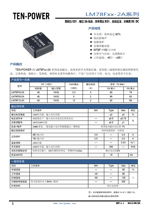
LM78Fxx-2A系列
高耐压 52V,输出 2A 电流,效率高达 92%,超低纹波,非隔离 DC-DC
机械尺寸 & 引脚功能
引脚功能
引脚
功能
1
Vin
2
GND
3
+Vout
4
GND
注: 1. 尺寸单位:mm[inch] 2. 引脚公差:±0.10mm[±0.004inch] 3. 未标注之公差:±0.25mm[±0.010inch]
测试输入/输出纹波噪声
推荐电路图
注:请使用BNC接头套在示波器的探头上,并在BNC上并联一个0.1uF的陶瓷电容。
外接电容 型号 LM78F03-2A LM78F05-2A LM78F12-2A
C1
10uF/100V 10uF/100V 10uF/100V
C2
100uF/6.3V 100uF/10V 47uF/16V
注:
1. 为了使电路工作在最佳状态,必须外接电容C1和C2,而且尽量靠近转换器的引脚端; 2. C1、C2的电容值请参照外接电容表,根据需要可适当加大,优先选用MLCC电容,若要使用电解电容,请选用低ESR的钽电容或高频电解电
LM78L05ACM三端稳压

LM78LXX Series3-Terminal Positive RegulatorsGeneral DescriptionThe LM78LXX series of three terminal positive regulators isavailable with several fixed output voltages making themuseful in a wide range of applications.When used as a zenerdiode/resistor combination replacement,the LM78LXX usu-ally results in an effective output impedance improvement oftwo orders of magnitude,and lower quiescent current.Theseregulators can provide local on card regulation,eliminatingthe distribution problems associated with single point regu-lation.The voltages available allow the LM78LXX to be usedin logic systems,instrumentation,HiFi,and other solid stateelectronic equipment.The LM78LXX is available in the plastic TO-92(Z)package,the plastic SO-8(M)package and a chip sized package(8-Bump micro SMD)using National’s micro SMD packagetechnology.With adequate heat sinking the regulator candeliver100mA output current.Current limiting is included tolimit the peak output current to a safe value.Safe areaprotection for the output transistors is provided to limit inter-nal power dissipation.If internal power dissipation becomestoo high for the heat sinking provided,the thermal shutdowncircuit takes over preventing the IC from overheating.Featuresn LM78L05in micro SMD packagen Output voltage tolerances of±5%over the temperaturerangen Output current of100mAn Internal thermal overload protectionn Output transistor safe area protectionn Internal short circuit current limitn Available in plastic TO-92and plastic SO-8low profilepackagesn No external componentsn Output voltages of5.0V,6.2V,8.2V,9.0V,12V,15Vn See AN-1112for micro SMD considerations Connection DiagramsSO-8Plastic(M)(Narrow Body)00774402Top View8-Bump micro SMD00774424Top View(Bump Side Down)(TO-92)Plastic Package(Z)00774403Bottom Viewmicro SMD Marking Orientation00774433Top ViewFebruary2005LM78LXXSeries3-TerminalPositiveRegulators ©2005National Semiconductor Corporation Ordering InformationPackageOrder Number Output VoltageNSC Drawing Supplied As microSMDLM78L05IBP5V BPA08AAB Reel of 250LM78L05IBPX 5V BPA08AAB Reel of 3000LM78L09ITP 9V TPA08AAA Reel of 250LM78L09ITPX9V TPA08AAA Reel of 3000SOIC NarrowLM78L05ACM 5V M08A Rail of 95LM78L05ACMX 5V M08A Reel of 2500LM78L12ACM 12V M08A Rail of 95LM78L12ACMX 12V M08A Reel of 2500LM78L15ACM 15V M08A Rail of 95LM78L15ACMX15V M08A Reel of 2500TO-92LM78L05ACZ 5V Z03A Box of 1800LM78L62ACZ 6.2V Z03A Box of 1800LM78L82ACZ 8.2V Z03A Box of 1800LM78L09ACZ 9V Z03A Box of 1800LM78L12ACZ 12V Z03A Box of 1800LM78L15ACZ15VZ03ABox of 1800L M 78L X X S e r i e s 2Absolute Maximum Ratings (Note 1)If Military/Aerospace specified devices are required,please contact the National Semiconductor Sales Office/Distributors for availability and specifications.Power Dissipation (Note 5)Internally LimitedInput Voltage 35VStorage Temperature −65˚C to +150˚CESD Susceptibility (Note 2)1kVOperating Junction Temperature SO-8,TO-920˚C to 125˚C micro SMD −40˚C to 85˚CSoldering InformationInfrared or Convection (20sec.)235˚CWave Soldering (10sec.)260˚C (lead time)LM78LXX Electrical CharacteristicsLimits in standard typeface are for T J =25˚C,Bold typefaceapplies over 0˚C to 125˚C for SO-8and TO-92packages,and −40˚C to 85˚C for micro SMD package.Limits are guaran-teed by production testing or correlation techniques using standard Statistical Quality Control (SQC)methods.Unless other-wise specified:I O =40mA,C I =0.33µF,C O =0.1µF.LM78L05Unless otherwise specified,V IN =10V Symbol ParameterConditionsMin Typ Max UnitsV OOutput Voltage4.855.2V7V ≤V IN ≤20V 1mA ≤I O ≤40mA (Note 3)4.755.251mA ≤I O ≤70mA (Note 3)4.755.25∆V O Line Regulation 7V ≤V IN ≤20V 1875mV8V ≤V IN ≤20V 1054∆V O Load Regulation 1mA ≤I O ≤100mA 20601mA ≤I O ≤40mA530I Q Quiescent Current 35mA ∆I Q Quiescent Current Change 8V ≤V IN ≤20V 1.01mA ≤I O ≤40mA 0.1V nOutput Noise Voltage f =10Hz to 100kHz (Note 4)40µV Ripple Rejectionf =120Hz8V ≤V IN ≤16V4762dB I PKPeak Output Current140mA Average Output Voltage TempcoI O =5mA−0.65mV/˚C V IN (Min)Minimum Value of Input VoltageRequired to Maintain Line Regulation 6.77V θJAThermal Resistance (8-Bump micro SMD)230.9˚C/W LM78L62ACUnless otherwise specified,V IN =12V Symbol ParameterConditionsMin Typ Max UnitsV OOutput Voltage5.956.26.45V8.5V ≤V IN ≤20V 1mA ≤I O ≤40mA (Note 3)5.96.51mA ≤I O ≤70mA (Note 3)5.96.5LM78LXX Series3LM78LXX Electrical Characteristics Limits in standard typeface are for T J =25˚C,Bold typefaceapplies over 0˚C to 125˚C for SO-8and TO-92packages,and −40˚C to 85˚C for micro SMD package.Limits areguaranteed by production testing or correlation techniques using standard Statistical Quality Control (SQC)methods.Unless otherwise specified:I O =40mA,C I =0.33µF,C O =0.1µF.(Continued)LM78L62AC(Continued)Unless otherwise specified,V IN =12VSymbol ParameterConditions MinTyp Max Units∆V O Line Regulation 8.5V ≤V IN ≤20V 65175mV 9V ≤V IN ≤20V 55125∆V O Load Regulation 1mA ≤I O ≤100mA 13801mA ≤I O ≤40mA640I Q Quiescent Current 25.5mA ∆I Q Quiescent Current Change 8V ≤V IN ≤20V 1.51mA ≤I O ≤40mA 0.1V nOutput Noise Voltage f =10Hz to 100kHz (Note 4)50µV Ripple Rejectionf =120Hz10V ≤V IN ≤20V4046dB I PKPeak Output Current140mA Average Output Voltage TempcoI O =5mA−0.75mV/˚C V IN (Min)Minimum Value of Input VoltageRequired to Maintain Line Regulation7.9V LM78L82ACUnless otherwise specified,V IN =14V Symbol ParameterConditionsMin Typ Max UnitsV OOutput Voltage7.878.28.53V11V ≤V IN ≤23V 1mA ≤I O ≤40mA (Note 3)7.88.61mA ≤I O ≤70mA (Note 3)7.88.6∆V O Line Regulation 11V ≤V IN ≤23V 80175mV12V ≤V IN ≤23V 70125∆V O Load Regulation 1mA ≤I O ≤100mA 15801mA ≤I O ≤40mA840I Q Quiescent Current 25.5mA ∆I Q Quiescent Current Change 12V ≤V IN ≤23V 1.51mA ≤I O ≤40mA 0.1V nOutput Noise Voltage f =10Hz to 100kHz (Note 4)60µV Ripple Rejectionf =120Hz12V ≤V IN ≤22V3945dB I PKPeak Output Current140mA Average Output Voltage TempcoI O =5mA−0.8mV/˚C V IN (Min)Minimum Value of Input VoltageRequired to Maintain Line Regulation9.9V L M 78L X X S e r i e s 4LM78LXX Electrical Characteristics Limits in standard typeface are for T J =25˚C,Bold typefaceapplies over 0˚C to 125˚C for SO-8and TO-92packages,and −40˚C to 85˚C for micro SMD package.Limits areguaranteed by production testing or correlation techniques using standard Statistical Quality Control (SQC)methods.Unless otherwise specified:I O =40mA,C I =0.33µF,C O =0.1µF.(Continued)LM78L09ACUnless otherwise specified,V IN =15V Symbol ParameterConditionsMin Typ Max UnitsV OOutput Voltage8.649.09.36V11.5V ≤V IN ≤24V 1mA ≤I O ≤40mA (Note 3)8.559.451mA ≤I O ≤70mA (Note 3)8.559.45∆V O Line Regulation 11.5V ≤V IN ≤24V 100200mV13V ≤V IN ≤24V 90150∆V O Load Regulation 1mA ≤I O ≤100mA 20901mA ≤I O ≤40mA1045I Q Quiescent Current 25.5mA ∆I Q Quiescent Current Change 11.5V ≤V IN ≤24V 1.51mA ≤I O ≤40mA0.1V nOutput Noise Voltage 70µV Ripple Rejectionf =120Hz15V ≤V IN ≤25V3844dB I PKPeak Output Current140mA Average Output Voltage TempcoI O =5mA−0.9mV/˚C V IN (Min)Minimum Value of Input VoltageRequired to Maintain Line Regulation10.7V LM78L12ACUnless otherwise specified,V IN =19V Symbol ParameterConditionsMin Typ Max UnitsV OOutput Voltage11.51212.5V14.5V ≤V IN ≤27V 1mA ≤I O ≤40mA (Note 3)11.412.61mA ≤I O ≤70mA (Note 3)11.412.6∆V O Line Regulation 14.5V ≤V IN ≤27V 30180mV16V ≤V IN ≤27V 20110∆V O Load Regulation 1mA ≤I O ≤100mA 301001mA ≤I O ≤40mA1050I Q Quiescent Current 35mA ∆I Q Quiescent Current Change 16V ≤V IN ≤27V 11mA ≤I O ≤40mA0.1V nOutput Noise Voltage 80µV Ripple Rejectionf =120Hz15V ≤V IN ≤254054dB I PKPeak Output Current140mA Average Output Voltage TempcoI O =5mA−1.0mV/˚C LM78LXX Series5LM78LXX Electrical Characteristics Limits in standard typeface are for T J =25˚C,Bold typefaceapplies over 0˚C to 125˚C for SO-8and TO-92packages,and −40˚C to 85˚C for micro SMD package.Limits areguaranteed by production testing or correlation techniques using standard Statistical Quality Control (SQC)methods.Unless otherwise specified:I O =40mA,C I =0.33µF,C O =0.1µF.(Continued)LM78L12AC(Continued)Unless otherwise specified,V IN =19VSymbol ParameterConditionsMinTyp Max Units V IN (Min)Minimum Value of Input VoltageRequired to Maintain Line Regulation13.714.5VLM78L15ACUnless otherwise specified,V IN =23V Symbol ParameterConditionsMin Typ Max UnitsV OOutput Voltage14.415.015.6V17.5V ≤V IN ≤30V 1mA ≤I O ≤40mA (Note 3)14.2515.751mA ≤I O ≤70mA (Note 3)14.2515.75∆V O Line Regulation 17.5V ≤V IN ≤30V 37250mV20V ≤V IN ≤30V 25140∆V O Load Regulation 1mA ≤I O ≤100mA 351501mA ≤I O ≤40mA1275I QQuiescent Current 35mA ∆I QQuiescent Current Change 20V ≤V IN ≤30V 11mA ≤I O ≤40mA0.1V nOutput Noise Voltage 90µV Ripple Rejectionf =120Hz18.5V ≤V IN ≤28.5V3751dB I PKPeak Output Current140mA Average Output Voltage TempcoI O =5mA−1.3mV/˚C V IN (Min)Minimum Value of Input VoltageRequired to Maintain Line Regulation16.717.5V Note 1:Absolute Maximum Ratings indicate limits beyond which damage to the device may occur.Electrical specifications do not apply when operating the device outside of its stated operating conditions.Note 2:Human body model,1.5k Ωin series with 100pF.Note 3:Power dissipation ≤0.75W.Note 4:Recommended minimum load capacitance of 0.01µF to limit high frequency noise.Note 5:Typical thermal resistance values for the packages are:Z Package:θJC =60˚C/W,=θJA =230˚C/W M Package:θJA =180˚C/Wmicro SMD Package:θJA =230.9˚C/WL M 78L X X S e r i e s 6Typical Performance CharacteristicsMaximum Average Power Dissipation (Z Package)Peak Output Current0077441400774416Dropout Voltage Ripple Rejection0077441700774418Output Impedance Quiescent Current0077441900774420LM78LXX Series7Typical Performance Characteristics(Continued)Quiescent Current00774421Equivalent CircuitLM78LXX00774407L M 78L X X S e r i e s 8Typical ApplicationsFixed Output Regulator00774408*Required if the regulator is located more than 3"from the power supply filter.**See (Note 4)in the electrical characteristics table.Adjustable Output Regulator00774409V OUT =5V +(5V/R1+I Q )R25V/R1>3I Q ,load regulation (L r )≈[(R1+R2)/R1](L r of LM78L05)Current Regulator00774410I OUT =(V OUT /R1)+I Q>I Q =1.5mA over line and load changes5V,500mA Regulator with Short Circuit Protection00774411*Solid tantalum.**Heat sink Q1.***Optional:Improves ripple rejection and transient response.Load Regulation:0.6%0≤I L ≤250mA pulsed with t ON =50ms.LM78LXX Series9Typical Applications(Continued)±15V,100mA Dual Power Supply00774412*Solid tantalum.Variable Output Regulator 0.5V-18V00774413*Solid tantalum.V OUT =V G +5V,R1=(−V IN /I Q LM78L05)V OUT =5V (R2/R4)for (R2+R3)=(R4+R5)A 0.5V output will correspond to (R2/R4)=0.1(R3/R4)=0.9L M 78L X X S e r i e s 10Physical Dimensions inches(millimeters)unless otherwise notedNOTES:UNLESS OTHERWISE SPECIFIED1.EPOXY COATING2.63Sn/37Pb EUTECTIC BUMP3.RECOMMEND NON-SOLDER MASK DEFINED LANDING PAD.4.PIN A1IS ESTABLISHED BY LOWER LEFT CORNER WITH RESPECT TO TEXT ORIENTATION.REMAINING PINS ARE NUMBERED COUNTERCLOCKWISE.5.XXX IN DRAWING NUMBER REPRESENTS PACKAGE SIZE VARIATION WHERE X1IS PACKAGE WIDTH,X2IS PACKAGE LENGTH AND X3IS PACKAGE HEIGHT.6.REFERENCE JEDEC REGISTRATION MO-211,VARIATION BC.8-Bump micro SMD for LM78L05IBP OnlyNS Package Number BPA08AABX1=1.285mm X2=1.285mm X3=0.850mm LM78LXX Series 11Physical Dimensionsinches (millimeters)unless otherwise noted (Continued)8-Bump micro SMD for LM78L09ITP OnlyNS Package Number TPA08AAAX1=1.285mm X2=1.285mm X3=0.500mmL M 78L X X S e r i e s 12Physical Dimensions inches(millimeters)unless otherwise noted(Continued)S.O.Package(M)NS Package Number M08ALM78LXXSeries 13Physical Dimensionsinches (millimeters)unless otherwise noted (Continued)Molded Offset TO-92(Z)NS Package Number Z03ANational does not assume any responsibility for use of any circuitry described,no circuit patent licenses are implied and National reserves the right at any time without notice to change said circuitry and specifications.For the most current product information visit us at .LIFE SUPPORT POLICYNATIONAL’S PRODUCTS ARE NOT AUTHORIZED FOR USE AS CRITICAL COMPONENTS IN LIFE SUPPORT DEVICES OR SYSTEMS WITHOUT THE EXPRESS WRITTEN APPROVAL OF THE PRESIDENT AND GENERAL COUNSEL OF NATIONAL SEMICONDUCTOR CORPORATION.As used herein:1.Life support devices or systems are devices or systems which,(a)are intended for surgical implant into the body,or (b)support or sustain life,and whose failure to perform when properly used in accordance with instructions for use provided in the labeling,can be reasonably expected to result in a significant injury to the user.2.A critical component is any component of a life support device or system whose failure to perform can be reasonably expected to cause the failure of the life support device or system,or to affect its safety or effectiveness.BANNED SUBSTANCE COMPLIANCENational Semiconductor manufactures products and uses packing materials that meet the provisions of the Customer Products Stewardship Specification (CSP-9-111C2)and the Banned Substances and Materials of Interest Specification (CSP-9-111S2)and contain no ‘‘Banned Substances’’as defined in CSP-9-111S2.National Semiconductor Americas Customer Support CenterEmail:new.feedback@ Tel:1-800-272-9959National SemiconductorEurope Customer Support CenterFax:+49(0)180-5308586Email:europe.support@Deutsch Tel:+49(0)6995086208English Tel:+44(0)8702402171Français Tel:+33(0)141918790National Semiconductor Asia Pacific Customer Support CenterEmail:ap.support@National SemiconductorJapan Customer Support Center Fax:81-3-5639-7507Email:jpn.feedback@ Tel:81-3-5639-7560L M 78L X X S e r i e s 3-T e r m i n a l P o s i t i v e R e g u l a t o r s。
开关型三端稳压器LM78xx-2A系列数据手册
电流 (mA)
2000 2000
2.5
2000
3.3
2000
5.0
2000
效率%(满载时)
Min
Max
Vin
Vin
81
78
82
79
86
84
88
87
91
90
输出特性表
项目 输出电压精度 线性调节率
负载调整率 纹波+噪声 短路保护 过热保护 输出限制电流 开关频率 动态负载稳定性 软启动时间 静态电流 温度系数 最大容性负载
25
80
mVp-p
可持续,自恢复
150
℃
5000
mA
300 340 380 KHz
±100 mV
15
ms
7
17
mA
±0.03 %/℃
1000 μF
产品选型
广州腾霄电子有限公司 地址:广州市天河区车陂路 8 号源利大厦 618。 电话/传真:020-28075080 /020-62824801
网址:www.ten‐
一般特性表
项目 存储湿度 工作温度 存储温度 工作时外壳温度 引脚耐焊接温度
冷却方式 外壳材料
工作条件
焊点距离外壳边沿 1.5mm,10 秒
Min
‐40 ‐55
Type
Max 95 85 125 100 300
自然空冷 阻燃耐热塑料(UL94‐V0)
单位 %
℃
1
REV:1.0 2011/11/15
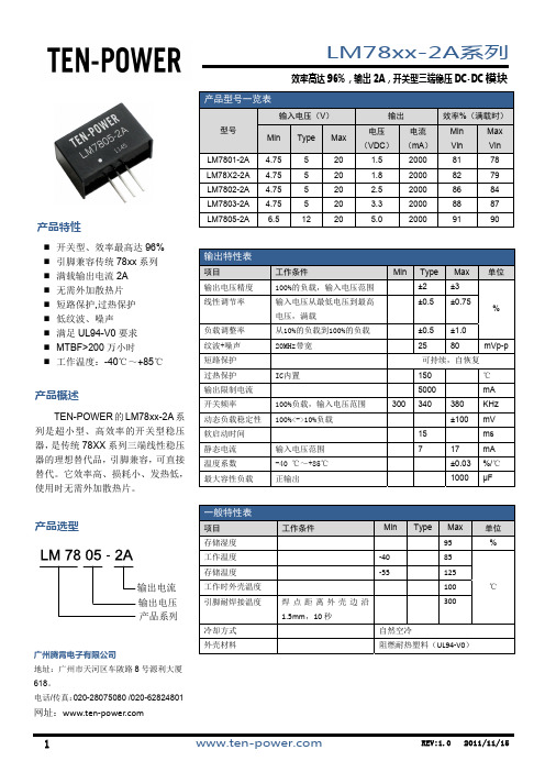
LM78xx-2A系列
效率高达 96%,输出 2A,开关型三端稳压 DC-DC 模块
纹波噪声(Iout=2A)
三端稳压器_ST 78M05
1/21January 2004s OUTPUT CURRENT TO 0.5AsOUTPUT VOLTAGES OF 5;6;8;9;12;15;18;20;24Vs THERMAL OVERLOAD PROTECTION s SHORT CIRCUIT PROTECTIONsOUTPUT TRANSITION SOA PROTECTIONDESCRIPTIONThe L78M00series of three-terminal positive regulators is available in TO-220,TO-220FP,DPAK and IPAK packages and with several fixed output voltages,making it useful in a wide range of applications.These regulators can provide local on-card regulation,eliminating the distribution problems associated with single point regulation.Each type employs internal current limiting,thermal shut-down and safe area protection,making it essentially indestructible.If adequate heat sinking is provided,they can deliver over 0.5A output current.Although designed primarily as fixed voltage regulators,these devices can beused with external components to obtainadjustable voltage and currents.L78M00SERIESPOSITIVE VOLTAGEREGULATORSL78M00SERIES2/21ABSOLUTE MAXIMUM RATINGSAbsolute Maximum Ratings are those values beyond which damage to the device may occur.Functional operation under these condition is not implied.THERMAL DATASHEMATIC DIAGRAMSymbol ParameterValue Unit V I DC Input Voltage (for V O =5to 18V)(for V O =20,24V)3540V V I O Output Current Internally Limited mA P D Power DissipationInternally Limited mW T stg Storage Temperature Range-65to +150°C T opOperating Junction Temperature Range0to +150°CSymbol ParameterTO-220TO-220FPDPAK IPAKUnit R thj-case Thermal Resistance Junction-case 358°C/W R thj-ambThermal Resistance Junction-ambient5060100°C/WL78M00SERIES3/21CONNECTION DIAGRAM (top view)ORDERING CODES(*)Available in Tape &Reel with the suffix "-TR".APPLICATION CIRCUITSTYPE TO-220TO-220FP DPAK (*)IPAK OUTPUT VOLTAGE L78M05L78M05CV L78M05CP L78M05CDT L78M05CDT-15V L78M06L78M06CV L78M06CP L78M06CDT L78M06CDT-16V L78M08L78M08CV L78M08CP L78M08CDT L78M08CDT-18V L78M09L78M09CV L78M09CP L78M09CDT L78M09CDT-19V L78M10L78M10CV L78M10CP L78M10CDT L78M10CDT-110V L78M12L78M12CV L78M12CP L78M12CDT L78M12CDT-112V L78M15L78M15CV L78M15CP L78M15CDT L78M15CDT-115V L78M18L78M18CV L78M18CP L78M18CDT L78M18CDT-118VL78M20L78M20CV L78M20CP L78M20CDT L78M20CDT-120V L78M24L78M24CVL78M24CPL78M24CDTL78M24CDT-124VL78M00SERIES4/21TEST CIRCUITS Figure 1:DC ParameterFigure 2:Load RegulationFigure 3:RippleRejectionL78M00SERIES5/21ELECTRICAL CHARACTERISTICS OF L78M05C (refer to the test circuits,T J =25°C,V I =10V,I O =350mA,C I =0.33µF,C O =0.1µF unless otherwise specified).ELECTRICAL CHARACTERISTICS OF L78M06C (refer to the test circuits,T J =25°C,V I =11V,I O =350mA,C I =0.33µF,C O =0.1µF unless otherwise specified).Symbol ParameterTest ConditionsMin.Typ.Max.Unit V O Output Voltage 4.85 5.2V V O Output Voltage I O =5to 350mA V I =7to 20V 4.7555.25V ∆V O Line Regulation V I =7to 25V I O =200mA 100mVV I =8to 25V I O =200mA 50∆V O Load Regulation I O =5to 500mA T J =25°C 100mV I O =5to 200mAT J =25°C50I d Quiescent Current 6mA ∆I dQuiescent Current ChangeI O =5to 350mA 0.5mA I O =200mAV I =8to 25V 0.8∆V O /∆T Output Voltage Drift I O =5mA T J =0to 125°C -0.5mV/°C SVR Supply Voltage Rejection V I =8to 18V f =120HzI O =300mA 62dB eN Output Noise Voltage B =10Hz to 100KHz 40µV V d Dropout Voltage 2V I scShort Circuit CurrentV I =35V300mA Symbol ParameterTest ConditionsMin.Typ.Max.Unit V O Output Voltage 5.756 6.25V V O Output Voltage I O =5to 350mA V I =8to 21V 5.766.3V ∆V O Line Regulation V I =8to 25V I O =200mA 100mVV I =9to 25V I O =200mA 50∆V O Load Regulation I O =5to 500mA T J =25°C 120mV I O =5to 200mAT J =25°C60I d Quiescent Current 6mA ∆I dQuiescent Current ChangeI O =5to 350mA 0.5mA I O =200mAV I =9to 25V 0.8∆V O /∆T Output Voltage Drift I O =5mA T J =0to 125°C -0.5mV/°C SVR Supply Voltage Rejection V I =9to 19V f =120HzI O =300mA 59dB eN Output Noise Voltage B =10Hz to 100KHz 45µV V d Dropout Voltage 2V I scShort Circuit CurrentV I =35V270mAL78M00SERIES6/21ELECTRICAL CHARACTERISTICS OF L78M08C (refer to the test circuits,T J =25°C,V I =14V,I O =350mA,C I =0.33µF,C O =0.1µF unless otherwise specified).ELECTRICAL CHARACTERISTICS OF L78M09C (refer to the test circuits,T J =25°C,V I =15V,I O =350mA,C I =0.33µF,C O =0.1µF unless otherwise specified).Symbol ParameterTest ConditionsMin.Typ.Max.Unit V O Output Voltage 7.788.3V V O Output Voltage I O =5to 350mA V I =10.5to 23V 7.688.4V ∆V O Line Regulation V I =10.5to 25V I O =200mA 100mVV I =11to 25V I O =200mA 50∆V O Load Regulation I O =5to 500mA T J =25°C 160mV I O =5to 200mAT J =25°C80I d Quiescent Current 6mA ∆I dQuiescent Current ChangeI O =5to 350mA 0.5mA I O =200mAV I =10.5to 25V 0.8∆V O /∆T Output Voltage Drift I O =5mAT J =0to 125°C-0.5mV/°C SVR Supply Voltage Rejection V I =11.5to 21.5V f =120Hz I O =300mA 56dB eN Output Noise Voltage B =10Hz to 100KHz 52µV V d Dropout Voltage 2V I scShort Circuit CurrentV I =35V250mA Symbol ParameterTest ConditionsMin.Typ.Max.Unit V O Output Voltage 8.6599.35V V O Output Voltage I O =5to 350mA V I =11.5to 24V 8.5599.45V ∆V O Line Regulation V I =11.5to 25V I O =200mA 100mVV I =12to 25V I O =200mA 50∆V O Load Regulation I O =5to 500mA T J =25°C 180mV I O =5to 200mAT J =25°C90I d Quiescent Current 6mA ∆I dQuiescent Current ChangeI O =5to 350mA 0.5mA I O =200mAV I =11.5to 25V 0.8∆V O /∆T Output Voltage Drift I O =5mA T J =0to 125°C -0.5mV/°C SVR Supply Voltage Rejection V I =12.5to 23V f =120HzI O =300mA 56dB eN Output Noise Voltage B =10Hz to 100KHz 58µV V d Dropout Voltage 2V I scShort Circuit CurrentV I =35V250mAL78M00SERIES7/21ELECTRICAL CHARACTERISTICS OF L78M10C (refer to the test circuits,T J =25°C,V I =16V,I O =350mA,C I =0.33µF,C O =0.1µF unless otherwise specified).ELECTRICAL CHARACTERISTICS OF L78M12C (refer to the test circuits,T J =25°C,V I =19V,I O =350mA,C I =0.33µF,C O =0.1µF unless otherwise specified).Symbol ParameterTest ConditionsMin.Typ.Max.Unit V O Output Voltage 9.61010.4V V O Output Voltage I O =5to 350mA V I =12.5to 25V 9.51010.5V ∆V O Line Regulation V I =12.5to 30V I O =200mA 100mVV I =13to 30V I O =200mA 50∆V O Load Regulation I O =5to 500mA T J =25°C 200mV I O =5to 200mAT J =25°C100I d Quiescent Current 6mA ∆I dQuiescent Current ChangeI O =5to 350mA 0.5mA I O =200mAV I =12.5to 30V 0.8∆V O /∆T Output Voltage Drift I O =5mA T J =0to 125°C -0.5mV/°C SVR Supply Voltage Rejection V I =13.5to 24V f =120HzI O =300mA 56dB eN Output Noise Voltage B =10Hz to 100KHz 64µV V d Dropout Voltage 2V I scShort Circuit CurrentV I =35V245mA Symbol ParameterTest ConditionsMin.Typ.Max.Unit V O Output Voltage 11.51212.5V V O Output Voltage I O =5to 350mA V I =14.5to 27V 11.41212.6V ∆V O Line Regulation V I =14.5to 30V I O =200mA 100mVV I =16to 30V I O =200mA 50∆V O Load Regulation I O =5to 500mA T J =25°C 240mV I O =5to 200mAT J =25°C120I d Quiescent Current 6mA ∆I dQuiescent Current ChangeI O =5to 350mA 0.5mA I O =200mAV I =14.5to 30V 0.8∆V O /∆T Output Voltage Drift I O =5mA T J =0to 125°C -1mV/°C SVR Supply Voltage Rejection V I =15to 25V f =120HzI O =300mA 55dB eN Output Noise Voltage B =10Hz to 100KHz 75µV V d Dropout Voltage 2V I scShort Circuit CurrentV I =35V240mAL78M00SERIES8/21ELECTRICAL CHARACTERISTICS OF L78M15C (refer to the test circuits,T J =25°C,V I =23V,I O =350mA,C I =0.33µF,C O =0.1µF unless otherwise specified).ELECTRICAL CHARACTERISTICS OF L78M18C (refer to the test circuits,T J =25°C,V I =26V,I O =350mA,C I =0.33µF,C O =0.1µF unless otherwise specified).Symbol ParameterTest ConditionsMin.Typ.Max.Unit V O Output Voltage 14.41515.6V V O Output Voltage I O =5to 350mA V I =17.5to 30V 14.251515.75V ∆V O Line Regulation V I =17.5to 30V I O =200mA 100mVV I =20to 30V I O =200mA 50∆V O Load Regulation I O =5to 500mA T J =25°C 300mV I O =5to 200mAT J =25°C150I d Quiescent Current 6mA ∆I dQuiescent Current ChangeI O =5to 350mA 0.5mA I O =200mAV I =17.5to 30V 0.8∆V O /∆T Output Voltage Drift I O =5mAT J =0to 125°C-1mV/°C SVR Supply Voltage Rejection V I =18.5to 28.5V f =120Hz I O =300mA 54dB eN Output Noise Voltage B =10Hz to 100KHz 90µV V d Dropout Voltage 2V I scShort Circuit CurrentV I =35V240mA Symbol ParameterTest ConditionsMin.Typ.Max.Unit V O Output Voltage 17.31818.7V V O Output Voltage I O =5to 350mA V I =20.5to 33V 17.11818.9V ∆V O Line Regulation V I =21to 33V I O =200mA 100mVV I =24to 33V I O =200mA 50∆V O Load Regulation I O =5to 500mA T J =25°C 360mV I O =5to 200mAT J =25°C180I d Quiescent Current 6mA ∆I dQuiescent Current ChangeI O =5to 350mA 0.5mA I O =200mAV I =21to 33V 0.8∆V O /∆T Output Voltage Drift I O =5mA T J =0to 125°C -1.1mV/°C SVR Supply Voltage Rejection V I =22to 32V f =120HzI O =300mA 53dB eN Output Noise Voltage B =10Hz to 100KHz 100µV V d Dropout Voltage 2V I scShort Circuit CurrentV I =35V240mAL78M00SERIES9/21ELECTRICAL CHARACTERISTICS OF L78M20C (refer to the test circuits,T J =25°C,V I =29V,I O =350mA,C I =0.33µF,C O =0.1µF unless otherwise specified).ELECTRICAL CHARACTERISTICS OF L78M24C (refer to the test circuits,T J =25°C,V I =33V,I O =350mA,C I =0.33µF,C O =0.1µF unless otherwise specified),Symbol ParameterTest ConditionsMin.Typ.Max.Unit V O Output Voltage 19.22020.8V V O Output Voltage I O =5to 350mA V I =23to 35V 192021V ∆V O Line Regulation V I =23to 35V I O =200mA 100mVV I =24to 35V I O =200mA 50∆V O Load Regulation I O =5to 500mA T J =25°C 400mV I O =5to 200mAT J =25°C200I d Quiescent Current 6mA ∆I dQuiescent Current ChangeI O =5to 350mA 0.5mA I O =200mAV I =23to 35V 0.8∆V O /∆T Output Voltage Drift I O =5mA T J =0to 125°C -1.1mV/°C SVR Supply Voltage Rejection V I =24to 34V f =120HzI O =300mA 53dB eN Output Noise Voltage B =10Hz to 100KHz 110µV V d Dropout Voltage 2V I scShort Circuit CurrentV I =35V240mA Symbol ParameterTest ConditionsMin.Typ.Max.Unit V O Output Voltage 232425V V O Output Voltage I O =5to 350mA V I =27to 38V 22.82425.2V ∆V O Line Regulation V I =27to 38V I O =200mA 100mVV I =28to 38V I O =200mA 50∆V O Load Regulation I O =5to 500mA T J =25°C 480mV I O =5to 200mAT J =25°C240I d Quiescent Current 6mA ∆I dQuiescent Current ChangeI O =5to 350mA 0.5mA I O =200mAV I =27to 38V 0.8∆V O /∆T Output Voltage Drift I O =5mA T J =0to 125°C -1.2mV/°C SVR Supply Voltage Rejection V I =28to 38V f =120HzI O =300mA 50dB eN Output Noise Voltage B =10Hz to 100KHz 170µV V d Dropout Voltage 2V I scShort Circuit CurrentV I =35V240mAL78M00SERIES10/21Figure 4:Dropout Voltage vs Junction TemperatureFigure 5:Dropout CharacteristicsFigure 6:Peak Output Current vs Input-Output Differential Voltage Figure 7:Output Voltage vs Junction TemperatureFigure 8:Supply Voltage Rejection vs FrequencyFigure 9:Quiescent Current vs JunctionTemperatureFigure10:Load Transient Response Figure11:Line Transient Response Figure12:Quiescent Current vs InputVoltage11/2112/21Figure 13:Fixed Output RegulatorNOTE:1.To specify an output voltage,substitute voltage value for "XX".2.Although no output capacitor is need for stability,it does improve transient response.3.Required if regulator is locate an appreciable distance from power supply filter.Figure 14:Figure 15:13/21Figure 16:Adjustable Output Regulator (7to 30V)Figure 17:0.5to 10V RegulatorFigure 18:High Current Voltage RegulatorFigure 19:High Output Current with ShortCircuit14/21Figure 20:Tracking Voltage RegulatorFigure 21:High Input Voltage CircuitFigure 22:Reducing Power Dissipation with DroppingResistor15/21Figure 23:Power AM Modulator (unity voltage gain,I O ≤ 0.5)NOTE:The circuit performs well up to 100KHz.Figure 24:Adjustable Output Voltage with Temperature CompensationNOTE:Q 2is connected as a diode in order to compensate the variation of the Q 1V BE with the temperature.C allows a slow risetime of the V O.L78M00SERIES Information furnished is believed to be accurate and reliable. However, STMicroelectronics assumes no responsibility for the consequences of use of such information nor for any infringement of patents or other rights of third parties which may result from its use. No license is granted by implication or otherwise under any patent or patent rights of STMicroelectronics. Specifications mentioned in this publication are subject to change without notice. This publication supersedes and replaces all information previously supplied. STMicroelectronics products are not authorized for use as critical components in life support devices or systems without express written approval of STMicroelectronics.The ST logo is a registered trademark of STMicroelectronicsAll other names are the property of their respective owners© 2004 STMicroelectronics - All Rights ReservedSTMicroelectronics GROUP OF COMPANIESAustralia - Belgium - Brazil - Canada - China - Czech Republic - Finland - France - Germany - Hong Kong - India - Israel - Italy - Japan - Malaysia - Malta - Morocco - Singapore - Spain - Sweden - Switzerland - United Kingdom - United States.21/21。
78系列集成稳压芯片的相关知识和缺点

78系列集成稳压芯片的相关知识和缺点2007年08月06日星期一上午09:56电子产品中常见到的三端稳压集成电路有正电压输出的78 ××系列和负电压输出的79××系列。
故名思义,三端IC是指这种稳压用的集成电路只有三条引脚输出,分别是输入端、接地端和输出端。
它的样子象是普通的三极管,TO- 220 的标准封装,也有9013样子的TO-92 封装。
用78/79系列三端稳压IC 来组成稳压电源所需的外围元件极少,电路内部还有过流、过热及调整管的保护电路,使用起来可靠、方便,而且价格便宜。
该系列集成稳压IC型号中的78或79后面的数字代表该三端集成稳压电路的输出电压,如7806表示输出电压为正6V,7909表示输出电压为负9V。
78/79系列三端稳压IC 有很多电子厂家生产,80年代就有了,通常前缀为生产厂家的代号,如TA7805是东芝的产品,AN7909是松下的产品。
(点击这里,查看有关看前缀识别集成电路的知识)有时在数字78或79后面还有一个M或L,如78M12或79L24,用来区别输出电流和封装形式等,其中78L调系列的最大输出电流为100mA ,78M系列最大输出电流为1A,78系列最大输出电流为1.5A。
它的封装也有多种,详见图。
塑料封装的稳压电路具有安装容易、价格低廉等优点,因此用得比较多。
79系列除了输出电压为负。
引出脚排列不同以外,命名方法、外形等均与78系列的相同。
因为三端固定集成稳压电路的使用方便,电子制作中经常采用,可以用来改装分立元件的稳压电源,也经常用作电子设备的工作电源。
电路图如图所示。
注意三端集成稳压电路的输入、输出和接地端绝不能接错,不然容易烧坏。
一般三端集成稳压电路的最小输入、输出电压差约为2V,否则不能输出稳定的电压,一般应使电压差保持在4-5V,即经变压器变压,二极管整流,电容器滤波后的电压应比稳压值高一些。
在实际应用中,应在三端集成稳压电路上安装足够大的散热器(当然小功率的条件下不用)。
- 1、下载文档前请自行甄别文档内容的完整性,平台不提供额外的编辑、内容补充、找答案等附加服务。
- 2、"仅部分预览"的文档,不可在线预览部分如存在完整性等问题,可反馈申请退款(可完整预览的文档不适用该条件!)。
- 3、如文档侵犯您的权益,请联系客服反馈,我们会尽快为您处理(人工客服工作时间:9:00-18:30)。
三端稳压块简介
三端稳压器比较
型号
输出电流 输出极性
输入输出压差
管脚排列
输出电压范围
78XX
78XX
1.5A +固定
2—3V
XX (V )
78MXX 500mA 78LXX 100 mA 79XX
79XX
1.5mA —固定
2—3V
XX (V )
79MXX 500mA 79LXX
100mA
LM317 0.1—1.5A +可调 <40V
1.2—37(V )
LM337 0.1—1.5A —可调 <40V
1.2—37(V )
衡量稳压电源的性能指标:
纹波系数:整流的目的是要得到直流电,因此输出的交流分量越小越好。
纹波系数γ=交流分量的总有效值 / 直流分量
电源内阻:指输入电压不变时,由负载的变化而引起的输出电压的变化与输出电流的变化之比。
即:
稳压系数:指负载不变,电网电压变化±10%(200V 或240V)时,输出的直流电压的相
对变化量与输入直流电压的相对变化量之比。
即:0'0|/=∆--=
=∆∆∆=O c
c c o
o o O c c o o u I u u u u u u I u u u u S 其中用晶体管毫伏表测量整流/滤波的交流分量;用万用电表的直流电压档测量直流电压分
量
00
00=∆∆∆-=i u I u
R。