Flash ROM ST25P16中文资料
flash_memory讲解

芯片封装技术
芯片封装形式主要以下几种:DIP,TSOP, PQFP,BGA,CLCC,LQFP,SMD,PGA, MCM,PLCC等。
DIP封装
定义: DIP封装(Dual In-line Package),也叫双列直插式 封装技术,双入线封装,DRAM的一种元件封装形 式 DIP封装具有以下特点:
图1 存储器系统示意图
图 2 Flash 存储器示图
Flash存储器的厂家
全球闪速存储器的技术主要掌握在AMD、 ATMEL、Fujistu、Hitachi、Hyundai、Intel、 Micron、Mitsubishi、Samsung、SHARP、 TOSHIBA,由于各自技术架构的不同,分为 几大阵营
NAND FLASH
特点: NAND技术Flash Memory具有以下特点:(1)以页为 单位进行读和编程操作,1页为256或512B(字 节);以块为单位进行擦除操作,1块为4K、8K或 16KB。具有快编程和快擦除的功能,其块擦除时间 是2ms;而NOR技术的块擦除时间达到几百ms。(2) 数据、地址采用同一总线,实现串行读取。随机读 取速度慢且不能按字节随机编程。(3)芯片尺寸小, 引脚少,是位成本(bit cost)最低的固态存储器,将 很快突破每兆字节1美元的价格限制。(4)芯片包含 有失效块,其数目最大可达到3~35块(取决于存储 器密度)
Flash Memory
Flash存储器的介绍 Flash存储器的厂家 Flash存储器的种类
定义:
1、 FLASH存储器又称闪存,它结合了 ROM和RAM的长处,不仅具备电子可擦除可 编程(EEPROM)的性能,还不会断电丢失数 据同时可以快速读取数据(NVRAM的优势), U盘和MP3里用的就是这种存储器。 2、对 Flash 存储器的操作一般是进行读、写 和擦除。Flash 存储器的擦除必须是以1KB 为单位对齐的地址并指定哪一区块被擦除, 或者全部擦除。
FM25L16_06中文资料
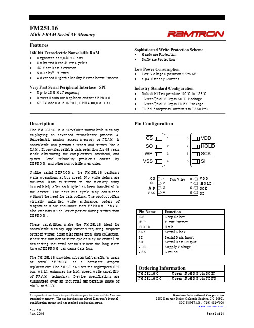
This product conforms to specifications per the terms of the Ramtron Ramtron International Corporationstandard warranty. The product has completed Ramtron’s internal1850 Ramtron Drive, Colorado Springs, CO 80921FM25L1616Kb FRAM Serial 3V MemoryFeatures16K bit Ferroelectric Nonvolatile RAM • Organized as 2,048 x 8 bits • Unlimited Read/Write Cycles • 45 Year Data Retention • NoDelay™ Writes• Advanced High-Reliability Ferroelectric ProcessVery Fast Serial Peripheral Interface - SPI • Up to 18 MHz Frequency• Direct Hardware Replacement for EEPROM • SPI Mode 0 & 3 (CPOL, CPHA=0,0 & 1,1)Sophisticated Write Protection Scheme • Hardware Protection • Software ProtectionLow Power Consumption• Low Voltage Operation 2.7-3.6V • 1 µA Standby CurrentIndustry Standard Configuration• Industrial Temperature -40°C to +85°C • “Green”/RoHS 8-pin SOIC Package • “Green”/RoHS 8-pin TDFN Package • TDFN Footprint Conforms to TSSOP-8DescriptionThe FM25L16 is a 16-kilobit nonvolatile memory employing an advanced ferroelectric process. A ferroelectric random access memory or FRAM is nonvolatile and performs reads and writes like a RAM. It provides reliable data retention for 45 years while eliminating the complexities, overhead, and system level reliability problems caused by EEPROM and other nonvolatile memories.Unlike serial EEPROMs, the FM25L16 performs write operations at bus speed. No write delays are incurred. Data is written to the memory array immediately after each byte has been transferred to the device. The next bus cycle may commence without the need for data polling. The product offers virtually unlimited write endurance, orders of magnitude more endurance than EEPROM. FRAM also exhibits much lower power during writes than EEPROM.These capabilities make the FM25L16 ideal for nonvolatile memory applications requiring frequent or rapid writes. Examples range from data collection, where the number of write cycles may be critical, to demanding industrial controls where the long write time of EEPROM can cause data loss.The FM25L16 provides substantial benefits to users of serial EEPROM as a hardware drop-in replacement. The FM25L16 uses the high-speed SPI bus, which enhances the high-speed write capability of FRAM technology. Device specifications are guaranteed over an industrial temperature range of -40°C to +85°C.Pin ConfigurationPin Name Function/CS Chip Select /WP Write Protect /HOLD Hold SCK Serial Clock SI Serial Data Input SO Serial Data Output VDD Supply Voltage VSS GroundOrdering InformationFM25L16-G “Green”/RoHS 8-pin SOIC FM25L16-DG “Green”/RoHS 8-pin TDFN/CS SO /WP VSSVDD /HOLD SCK SIOverviewThe FM25L16 is a serial FRAM memory. The memory array is logically organized as 2,048 x 8 and is accessed using an industry standard Serial Peripheral Interface or SPI bus. Functional operation of the FRAM is similar to serial EEPROMs. The major difference between the FM25L16 and a serial EEPROM with the same pinout is the FRAM’s superior write performance.Memory ArchitectureWhen accessing the FM25L16, the user addresses 2,048 locations of 8 data bits each. These data bits are shifted serially. The addresses are accessed using the SPI protocol, which includes a chip select (to permit multiple devices on the bus), an op-code, and a two-byte address. The upper 5 bits of the address range are ‘don’t care’ values. The complete address of 11-bits specifies each byte address uniquely.Most functions of the FM25L16 either are controlled by the SPI interface or are handled automatically by on-board circuitry. The access time for memory operation is essentially zero, beyond the time needed for the serial protocol. That is, the memory is read or written at the speed of the SPI bus. Unlike an EEPROM, it is not necessary to poll the device for a ready condition since writes occur at bus speed. So, by the time a new bus transaction can be shifted into the device, a write operation will be complete. This is explained in more detail in the interface section. Users expect several obvious system benefits from the FM25L16 due to its fast write cycle and high endurance as compared with EEPROM. In addition there are less obvious benefits as well. For example in a high noise environment, the fast-write operation is less susceptible to corruption than an EEPROM since it is completed quickly. By contrast, an EEPROM requiring milliseconds to write is vulnerable to noise during much of the cycle.Note that the FM25L16 contains no power management circuits other than a simple internal power-on reset. It is the user’s responsibility to ensure that V DD is within datasheet tolerances to prevent incorrect operation. It is recommended that the part is not powered down with chip select active.Serial Peripheral Interface – SPI BusThe FM25L16 employs a Serial Peripheral Interface (SPI) bus. It is specified to operate at speeds up to 18 MHz. This high-speed serial bus provides high performance serial communication to a host microcontroller. Many common microcontrollers have hardware SPI ports allowing a direct interface. It is quite simple to emulate the port using ordinary port pins for microcontrollers that do not. The FM25L16 operates in SPI Mode 0 and 3.The SPI interface uses a total of four pins: clock, data-in, data-out, and chip select. A typical system configuration uses one or more FM25L16 devices with a microcontroller that has a dedicated SPI port, as Figure 2 illustrates. Note that the clock, data-in, and data-out pins are common among all devices. The Chip Select and Hold pins must be driven separately for each FM25L16 device.For a microcontroller that has no dedicated SPI bus, a general purpose port may be used. To reduce hardware resources on the controller, it is possible to connect the two data pins (SI, SO) together and tie off (high) the Hold pin. Figure 3 shows a configuration that uses only three pins.Protocol OverviewThe SPI interface is a synchronous serial interface using clock and data pins. It is intended to support multiple devices on the bus. Each device is activated using a chip select. Once chip select is activated by the bus master, the FM25L16 will begin monitoring the clock and data lines. The relationship between the falling edge of /CS, the clock and data is dictated by the SPI mode. The device will make a determination of the SPI mode on the falling edge of each chip select. While there are four such modes, the FM25L16 supports Modes 0 and 3. Figure 4 shows the required signal relationships for Modes 0 and 3. For both modes, data is clocked into the FM25L16 on the rising edge of SCK and data is expected on the first rising edge after /CS goes active. If the clock begins from a high state, it will fall prior to beginning data transfer in order to create the first rising edge. The SPI protocol is controlled by op-codes. These op-codes specify the commands to the device. After /CS is activated the first byte transferred from the bus master is the op-code. Following the op-code, any addresses and data are then transferred. Note that the WREN and WRDI op-codes are commands with no subsequent data transfer.Important: The /CS must go inactive (high) after an operation is complete and before a new op-code can be issued. There is one valid op-code only per active chip select.。
M25P80的介绍
1引言FPGA凭借其方便灵活、可重复编程等优点而日益被广泛应用;闪速存储器(Flash Memo ry)以其集成度高、成本低、使用方便等优点,在众多领域中也获得了广泛应用。
在现代数字电路设计中。
经常需要保存大量数据,而Flash存储速度快、体积小、功耗低且价格低廉,可在线电擦写,信息在掉电后不会丢失,因此成为设计人员的首选。
2 M25P80的介绍Flash是一种具有电可擦除的可编程ROM,可以分为两大类:并行Flash和串行Flash。
并行Flash存储量大,速度快;而串行Flash存储量相对较小,但体积小,连线简单,可减小电路面积,节约成本,二者各有其优缺点,可依据实际需要选取。
本文开发的系统对速度的要求不是很高,而对电路板的面积要求则较为苛刻,因此系统设计选用了串行FlashM25P80。
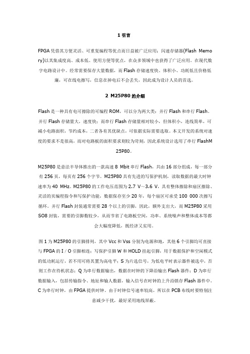
M25P80是意法半导体推出的一款高速8 Mbit串行Flash,共由16部分组成,每一部分有256页,每页有256个字节。
M25P80具有先进的写保护机制,读取数据的最大时钟速率为40 MHz。
M25P80的工作电压范围为2.7 V~3.6 V,具有整体擦除和扇区擦除、灵活的页编程指令和写保护功能,数据保存至少20年,每个扇区可承受100 000次擦写循环。
并行Flash封装通常需要28个以上的引脚,因此,额外支出大,而M25P80采用SO8封装,需要的引脚数较少,从而节省了电路板空间,功率、系统噪声和整体成本等都会大幅度降低,既经济又实用。
图1为M25P80的引脚排列,其中Vcc和Vss分别为电源和地,其他6个引脚均可直接与FPGA的I/O引脚相连;写保护引脚W和HOLD挂起引脚,用于数据保护和空闲模式的低功耗运行,若不用可将其置为高电平;S为片选信号,为低电平时表示器件被选中,否则工作在待机状态;Q为串行数据输出,数据在时钟的下降沿输出Flash器件;D为串行数据输入,包括传输指令、地址和输人数据,输入信号在时钟的上升沿锁存Flash器件中。
Xilinx FPGA 中文手册-《Platform Flash PROM User Guide》中文版

《Platform Flash PROM User Guide》中文版FPGA的配置分为主串行和从串行两种,差别在于时钟源不同。
nCF为高时PROM的DO数据有效,nCE和OE使能。
P24和26介绍了接线图和引脚功能。
原型开发优势每写一次可以有4套不同的程序进行测试。
板子测试配置或安全升级设计的版本中写有诊断程序,如果发现原程序不满足要求,可以调用符合要求的程序重新执行,节省了调试时间。
PlatForm具有备份程序的功能。
防止不完整或损坏数据FPGA的所有IO口在DONE为低电平时均不可用,PlatForm满足这个要求。
为什么使用内部解压或晶振Platform PROM片上解压使得用户可以多存储50%的数据。
Platform PROM提供20MHz或者40MHz(默认)的时钟用于将配置数据从PROM送入FPGA。
内部晶振,特别是40MHz的操作只应用于解压模式。
否则,FPGA的CCLK或者外部晶振会用于驱动。
PROM的解压输出数据速率为内部时钟的一半,换言之,解压数据流配置时间是非压缩数据流的两倍。
如果需要快速配置,FPGA的BitGen-g compress方式可以作为压缩模式。
时钟CLKOUT信号在配置过程中,且在nCE低、OE/nRESET高时有效;无效时呈高组态并且需要外部上拉以避免不确定状态。
时钟速率可以配置,默认为1MHz,可以为1,3,6,12等,XCFxxS最大为33MHz。
PROM文件生成和烧写.bit(Bitstream)文件为输入数据流,.mcs文件为输出数据,.cfi文件为配置格式信息文件。
.bit文件为FPGA使用的二进制数据,.mcs文件为PROM运行文件,.cfi(Configuration format information)文件名字与前两者根目录相同。
标准的PROM文件为前两者。
在XCFxxP系列PROM使用多版本程序设计、CLKOUT、解压缩等功能时还需要使用.cfi文件。
PIC16f877中文资料1
PIC16F877原理简介1.1 PIC16F877特性:PIC16F877是由Microchip公司所生产开发的新产品,属于PICmicro系列单片微机,具有Flash program程序内存功能,可以重复烧录程序,适合教学、开发新产品等用途;而其内建ICD(In Circuit Debug)功能,可以让使用者直接在单片机电路或产品上,进行如暂停微处理器执行、观看缓存器内容等,让使用者能快速地进行程序除错与开发。
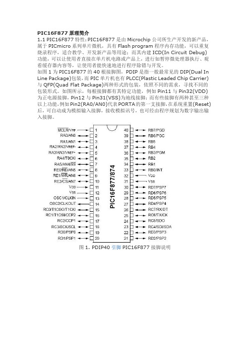
如图1为PIC16F877的40根接脚图,PDIP是指一般最常见的DIP(Dual In Line Package)包装,而PIC单片机也有PLCC(Plastic Leaded Chip Carrier)与QFP(Quad Flat Package)两种形式的包装,依照不同的需求,寻找不同的包装形式。
如图所示,每根接脚都有其特定功能,例如Pin11与Pin32(VDD)为正电源接脚,Pin12与Pin31(VSS)为地线接脚;而有些接脚有两种甚至三种以上功能,例如Pin2(RA0/AN0)代表PORTA的第一支接脚,在系统重置(Reset)后,可自动成为模拟输入接脚,接收模拟讯号,也可经由程序规划为数字输出输入接脚。
图1. PDIP40引脚PIC16F877接脚说明图2. PDIP28和SOIC28引脚PIC16F877接脚图说明图3. PLCC44引脚PIC16F877脚位图说明图4. QFP44引脚PIC16F877引脚图说明PIC16F877属于闪控式(Flash)单片机,可以重复烧录,其ROM的容量总共是8K words,以2K为一个page,区分为4个pages;内部RAM总共有512个字节(00f~1FFh),以128个字节为一个Bank,共区分为4个Bank,如图5所示,每个Bank的前半段都有其特殊用途,分别连接到其特殊功能模块,例如I/O、CCP、Timer、USART、MSSP等。
EN25QH16-104HIP中文资料(Eon Silicon)中文数据手册「EasyDatasheet - 矽搜」
3
VSS
4
8 VCC 7 HOLD# (DQ 3) 6 CLK 5 DI (DQ 0)
8 - 引脚SOP / PDIP
CS# 1 DO (DQ 1) 2 WP# (DQ 2) 3
VSS 4
8 VCC 7 HOLD# (DQ 3) 6 CLK 5 DI (DQ 0)
8 - 铅VDFN
芯片中文手册,看全文,戳
可锁定512字节OTP安全部门
支持串行闪存可发现 参数(小农发展方案)签名
阅读唯一ID号 最低100K耐久性周期
封装选项 - 8引脚SOP 150mil体宽 - 8引脚SOP 200mil体宽 - 8接触VDFN(5x6mm) - 8引脚PDIP - 24球TFBGA封装(6x8mm)
- 所有无铅封装符合RoHS标准
顶 视 图 ,球 朝 下
EN25QH16
24 - 球TFBGA
芯片中文手册,看全文,戳
图 2.框 图
EN25QH16
Note: 1. DQ 0 和DQ 1 用于双核和四核指令. 2. DQ 0 ~ DQ 3 用于四路说明.
芯片中文手册,看全文,戳
表 1.引 脚 名 称
该EN25QH16被设计为允许任何单
扇区/块
在同一时间或整片擦除操作.
该EN25QH16可以被配置为防护护存储器作为软件防护护模式一部分.该
设备可以维持一个最低100K编程/擦除周期每一个扇区
或块 .
芯片中文手册,看全文,戳
图一接线图
EN25QH16
CS#
1
DO (DQ 1)
2
WP# (DQ 2)
芯片中文手册,看全文,戳
EN25QH16
16兆 位 串 行 闪 存 与 4K字 节 统 一 部 门
SmartRF flash programmer中文手册
SmartRF(TM)闪存编程器用户手册SmartRF(TM)Flash Programmer User Manual杨熙贤翻译(2015.5.1)内容1引言 (1)2关于本手册 (2)3定义 (3)4安装 (4)5用GUI版本编程 (5)5.1 CCXXX SoC或MSP430设备编程 (5)5.1.1片上系统 (6)5.1.2MSP430编程 (11)5.2评估板编程 (12)5.2.1USB微控制器固件更新 (12)5.2.2评估板的固件自动更新 (13)5.2.3 EB引导装载程序 (15)6命令行界面 (17)6.1选项 (17)6.2 IAR工作台插件 (17)6.2.1安装 (17)6.2.2使用 (18)7安装HEX文件 (21)8故障排除 (21)9文档历史记录 (22)1 引言这是SmartRF闪存编程器用户手册。
闪存编程器可对德州仪器公司低功率射频片上系统的闪存进行编程,并可通过MSP-FET430UIF对MSP430器件闪存和eZ430加密狗进行编程。
对于IEEE802.15.4兼容设备(如CC2530)和Bluetooth®低能量设备(例如CC2540)来说,闪存编程器可向其中读取和写入IEEE/MAC地址。
此外,闪存编程器还可用于升级SmartRF04EB、SmartRF05EB、CC Debugger和CC2430DB上的固件。
2 关于本手册本手册涵盖Flash编程器的使用,包括GUI版本和命令行界面,手册中介绍了最常用的功能和相关选项。
第5.2节描述如何从IAR Embedded Workbench中用闪存编程器命令行界面如同闪存编程那样执行构建后的操作。
Flash编程器具有用Silicon Laboratories的串行适配器EC2对SmartRF04EB和CC2430DB上的USB MCU进行编程的功能,但这不包括在本手册内。
3 定义4 安装下载并解压TI网页(/tool/flash-programmer)上的zip文件。
W25X16中文手册
引封W25X16 W25X32 W25X64 FLASH PCB FLASH 2.7V~3.6V 0.5 1W25X16 W25X32 W25X64 8192 16384 32768 256 256 sector 16 (block) 256 W25X16 W25X32 W25X64 512 1024 2048 32 64 128W25X16 W25X32 W25X64 SPI 75MHz CLKCSDODIODIO DI Fast Read Dual Output instruction DO DOHOLD WP bit1 JEDEC态封FLASHW25X16 16M bit /2M byteW25X32 32M bit /4M byteW25X64 64M bit /8M byte2564K Sectors 64K (Blocks)SPIClock CS DIO DO HOLD SPI150M75M4KB4K64K256 < 210202.7V~3.6V0.5 1-40°C ~ +8挥°点WP8 (pin)SOIC 208mil W25X16,X328 (pin)PDIP 300mil W25X16,X32,X64 16 (pin)SOIC 300mil W25X16,X32,X64 8 (pad) WSON 提×5mm W25X168 (pad) WSON 明×6mm W25X32,X64 总封脚类IC 态0时m除lW25X16,W25X32 4封W脚类N 描×指MMW25X16指封PDIP 总00MI程W25X16,W25X32,W25X64描封 脚类IC 态0时m除l PDIP 总00m除l W脚类N 描×指MMPAD封N类 PAD封NAM状 I/类 F芯NCTI类N1 /CS I2 DO O3 /WP I4 GND5 DIO I/O /6 CLK I7 /HOLD I8 VCC擦封脚类IC 总00m除lW25X16,W25X32,W25X64时封脚类IC 总00m除lPAD封N类 PAD封NAM状 I/类 F芯NCTI类N1 /HOLD I2 VCC3 N/C4 N/C5 N/C6 N/C7 /CS I8 DO O9 /WP I10 GND11 N/C12 N/C13 N/C14 N/C15 DIO I/O16 CLK I时封引时封态 /C脚CS CS DO CS CS CS时封总 D类时封4 /WP时封指 /留类程DCS HOLD DO DIO CLK HOLD SPI时封描 C程KSPI时封擦 / DI类DIO CLK Fast Read Dual Output9封引0封引0封引 脚PI引0封引封引 脚PIW25X16\X32\X64 SPI CLK\CS\DIO\DO SPI 0 0 0 3 1 1 0 3 SPI SPI CLK 0 CLK 3 CLK CLK引0封引封态 脚PIW25X16\X32X64 SPI Fast Read Dual Output 0x3B SPI code-shadowing cache code-segments to RAM for execution DIO引0封引封总 /留类程DCS=0 HOLD SPI SPI SPI SPI SPI page buffer SPI SPICS HOLD CLK CLK CLK HOLD CLK CLK CLKDO DIO DO CS CS引0封态 /W置引0封态封引VCC/WPVCC (VWI) VCC (VWI) tpuw Write Enable Page Program Sector Erase Block Erase Chip Erase Write Status Register CS VCC VCCVCCmin TVSL CSWEL 0 WEL 0SPR TB,BP2,BP1,BP0 /WP引引封S7 S6 S5 S4 S3 S2 S1 S0SRP (Reservd) TB BP2 BP1 BP0 WEL BUSY引引封引引引封引封引 B芯脚YBUSY S0 1 0引引封引封态 W状程WEL S1 1 0引引封引封总 BP态,BP引,BP0BP2\BP1\BP0 S4\S3\S2 0 SPR 1 /WP引引封引封4 TBTB S5 0 SPR 1 /WP引引封引封指S6 0引引封引封描 脚置PSRP S7 /WP 0 SRP =0 /WP SRP =1 /WP =0 SRP =1 /WP =1引引封引封擦引引封态W25X16\X32\X64 15 15 SPI /CS DIODIOdummy bytes /CS引引封态封引引引封态封态12 3 4 5 6 06h04h05h (S7~S0)01h S7~S003h A23~A16 A15~A8 A7~A0 (D7~D0)0Bh A23~A16 A15~A8 A7~A0 D7~D03Bh A23~A16 A15~A8 A7~A0 I/O=(D6,D4,D2,D0)O=(D7,D5,D3,D1)02h A23~A16 A15~A8 A7~A0 (D7~D0) 25664K D8h A23~A16 A15~A8 A7~A0(4K) 20h A23~A16 A15~A8 A7~A0C7hB9h/IDABh (ID7~ID0)/ ID 90h 00h (M7~M0) (ID7~ID0)JEDEC ID 9Fh (M7~M0) (ID15~ID8) (ID7~ID0)1. DO引引封态封总 0描h Wr除te 状na造leWEL WEL /CS06h DI CLK /CS引引封态封4 04h Wr除te D除sa造leWEL 0 /CS 04h DIO /CS WEL 0引引封态封指 0指h 置ea释 脚tatus 置e钟除ster/CS 05h DIO CLK 05h DO CLKBUSY /CS DO /CS个引引封态封描 0引h Wr除te 脚tatus 置e钟除ster/CS 01h DIO DIO /CS /CSSRP TB BP2 BP1 BP0 BUSY 1 BUSY 0 WEL 0TB BP2 BP1 BP0 1 SRP 1 /WP引引封态封擦 0总h 置ea释 Data属点脚 带意阀 然看系 性或 点程磁 性或 点程磁 然系 然系 属点脚 个引引封态封时 0Bh Fast 置ea释属点脚 带激阀 然看系 性或 然看系 明 然系 个个个11.2.9 3Bh Fast Read Dual Output然看 然看系 脚P看 个属点脚 意激阀 然看系 性或 然看系 明 然系 然看系 然看系 然系引引封态封引0 0态h Pa钟e Pro钟ram1 /CS 02h DIO 24 /CS性挥提 带 性挥提 性挥提 性挥提 性挥提 个 激范脚虑 引 激范脚虑带 个引引封态封引引 态0h 脚e部tor 状rase或磁 引 环环阀 W状程 引 个 属点脚 性带阀 然看系 性或 属点脚 属点脚 激范脚虑 引 激范脚虑 带 W状程 带 个引引封态封引态 D时h Blo部页 状rase64K 1 FFh/CS D8h DIO 24 /CS /CS BUSY 1BUSY 0 WEL 0 个个引引封态封引总 C擦h Ch除p 状rase1 FFh/CS C7h DIO /CS /CS BUSY BUSY 1 BUSY 0 WEL 0 BP2\BP1\BP0引引封态封引4 B9h Power-释own属点脚 激未阀 然看系 属点脚 属 看然 个引引封态封引指 / ID ABh 置elease Power-释own/Dev除部e ID ID/CS ABh DIO /CS tRES1/ ID引引封态封引描 / 90h 置ea释 Manufa部ture/Dev除部e ID / / ID / JEDEC ID属点脚 未带阀 然看系 性或 带带带带带带阀 看然 看然 然系 点程磁性或 带带带带带引阀 看然 看然 看然 看然 明 个个属 看然 个引引封态封引擦 J状D状C ID 9FhW25X16/X32/X64 ID/CS 9Fh DIO ID ID ID DO CLK ID 8ID Manufa部turer an释 Dev除部e I释ent除f除部at除onration W25X16 ration ARM Cortex-M0 。
SST25VF080B 中文手册
8兆位的SPI串行闪存A Microchip Technology CompanySST25VF080BSST公司的25系列串行闪存系列具有四线SPI兼容跨面对这允许一个低引脚数封装占用的电路板空间并最终降低总系统成本.该SST25VF080B设备加强与改进工作频率从而降低功耗化. SST25VF080B SPI串行闪存采用SST公司生产的专有的,高性能CMOS SuperFlash技术.分裂闸电池设计和厚氧化物隧道喷油器达到更好的可靠性和马努-与其他方法相比facturability产品特点:•单电压读写操作– 2.7-3.6V•自动地址递增(AAI)编程- 降低整个芯片的编程时间超过字节亲克操作•串行接口架构- 兼容SPI:模式0和模式3写操作结束的•检测- 软件轮询状态寄存器中的BUSY位- SO引脚在AAI模式上忙状态读出•高速时钟频率- 50/66号MHz的条件(见表15)- (SST25VF080B-50-xx-xxxx)- 80 MHz的- (SST25VF080B-80-xx-xxxx)•保持引脚(HOLD#)- 挂起一个串行序列的记忆没有取消选择该设备•卓越的可靠性- 耐力:100,000周期(典型值)- 大于100年数据保存期•写保护(WP#)- 启用/禁用状态的锁断功能注册•低功耗:- 有效的读电流:10 mA(典型值)- 待机电流:5μA(典型值)•软件写保护- 通过写块保护位的保护状态注册•灵活的擦除功能- 统一的4 K字节部门- 统一32 K字节块重叠- 统一64 K字节块重叠•温度范围- 商业:0°C至+70°C- 工业级:-40°C至+85°C•快速擦除和字节编程:- 芯片擦除时间:35 ms(典型值)- Sector-/Block-Erase时间:18毫秒(典型值)- 字节编程时间:7μs(典型值)•可用的软件包- 8引脚SOIC(200密耳)- 8引脚SOIC(150密耳)- 8触点WSON(6毫米×5毫米)- 8引脚PDIP(300密耳)产品描述SST公司的25系列串行闪存系列具有四线SPI兼容接口,允许低引脚数封装占用的电路板空间,并最终降低总系统成本.该SST25VF080B设备加强与改进工作频率和更低的功耗,化. SST25VF080B SPI串行闪存采用SST专有的,高性生产曼斯CMOS SuperFlash技术.分裂门电池设计和厚氧化物隧道注射器实现更高的可靠性和可制造性与替代方法.该SST25VF080B器件显著提高性能和可靠性,同时降低功耗消费.该设备写(编程或擦除)与2.7-3.6V的单电源供电SST25VF080B.所消耗的总能量是所施加的电压,电流和应用的时间的函数.因为对于任何给定的电压范围,SuperFlash技术使用较少的编程电流和有一个较短的擦除时间,在任何擦除或编程操作消耗的总能量小于其他闪存技术.该SST25VF080B器件采用8引脚SOIC提供(200密耳),8引脚SOIC(150密耳),8 - 接触WSON(6毫米×5毫米),和8引脚PDIP(300密耳)封装.参见图2引脚分配存储器结构该SST25VF080B超快闪存储器阵列的统一4 K字节可擦除扇区32K字节覆盖块和64 K字节覆盖可擦除块.设备操作该SST25VF080B通过SPI(串行外设接口)总线兼容的协议来访问.SPI总线包括四个控制线;芯片使能(CE#)用于选择该设备,数据通过串行数据输入(SI),串行数据输出(SO)和串行时钟(SCK)进行访问.该SST25VF080B支持模式0(0,0)和模式3(1,1)SPI总线操作.所不同的在两个模式之间,如图3所示,是在SCK信号的状态时,该总线主机在待机模式并没有数据正在传输. SCK信号是低模式0和SCK信号为高电平模式3.对于这两种模式,串行数据输入(SI)进行采样,在SCK时钟信号和串行数据输出的上升沿(SO)后驱动在SCK时钟信号的下降沿.保持操作在按住#引脚用于暂停串行序列正在进行与SPI闪存没有复位,婷定时序列.要启动按住#模式,CE#必须在低电平状态.在HOLD#模式时,SCK低电平状态恰逢HOLD#信号的下降沿开始.该HOLD模式当HOLD#信号的上升沿与SCK低电平状态恰逢结束.如果HOLD#信号的下降沿不与SCK低电平状态,则设备一致进入保持模式当SCK未来达到低电平状态.类似地,如果在上升沿HOLD#信号不与SCK低电平状态保持一致,然后在保持模式器件退出当SCK未来达到低电平状态.参见图4为保持状态的波形.一旦设备进入保持模式,因此将在高阻抗状态,而SI和SCK可以VIL或VIH.如果CE#是在一个保持状态驱动的主动高,它重置设备的内部逻辑.只要HOLD#信号为低,内存仍然在保持状态.要恢复与设备通信,按住#必须积极推动高,CE#必须被驱动低电平有效.参见图24为保持时间。
ATF16V8BQL-25PC中文资料
Features•Industry Standard Architecture–Emulates Many 20-Pin P ALs®–Low Cost Easy-to-Use Software Tools•High-Speed Electrically Erasable Programmable Logic Devices –7.5 ns Maximum Pin-to-Pin Delay•Several Power Saving Options•CMOS and TTL Compatible Inputs and Outputs–Input and I/O Pull-Up Resistors•Advanced Flash Technology–Reprogrammable–100% Tested•High Reliability CMOS Process–20 Year Data Retention–100 Erase/Write Cycles–2,000V ESD Protection–200 mA Latchup Immunity•Commercial, and Industrial Temperature Ranges•Dual-in-Line and Surface Mount Packages in Standard Pinouts Block DiagramDevice I CC, Stand-By I CC, ActiveA TF16V8B50 mA55 mAA TF16V8BQ35 mA40 mAA TF16V8BQL 5 mA20 mATSSOP T op ViewDescriptionThe ATF16V8B is a high performance CMOS (Electrically Erasable) Programmable Logic Device (PLD) which utilizes Atmel’s proven electrically erasable Flash memory technol-ogy. Speeds down to 7.5 ns are offered. All speed ranges are specified over the full 5V ± 10% range for industrial temperature ranges, and 5V ± 5% for commercial tempera-ture ranges.Several low power options allow selection of the best solu-tion for various types of power-limited applications. Each ofthese options significantly reduces total system power and enhances system reliability.The ATF16V8Bs incorporate a superset of the generic architectures, which allows direct replacement of the 16R8family and most 20-pin combinatorial PLDs. Eight outputs are each allocated eight product terms. Three different modes of operation, configured automatically with soft-ware, allow highly complex logic functions to be realized.Absolute Maximum Ratings*T emperature Under Bias.................................-55o C to +125o C *NOTICE:Stresses beyond those listed under “Absolute Maximum Ratings” may cause permanent dam-age to the device. This is a stress rating only and functional operation of the device at these or any other conditions beyond those indicated in the operational sections of this specification is not implied. Exposure to absolute maximum rating conditions for extended periods may affect device reliability.Note:1.Minimum voltage is -0.6V DC, which may under-shoot to -2.0V for pulses of less than 20 ns. Max-imum output pin voltage is V CC + 0.75V DC, which may overshoot to 7.0V for pulses of less than 20 ns.Storage T emperature......................................-65o C to +150o C Voltage on Any Pin withRespect to Ground .......................................-2.0 V to +7.0 V (1)Voltage on Input Pins with Respect to GroundDuring Programming...................................-2.0 V to +14.0 V (1)Programming Voltage withRespect to Ground .....................................-2.0 V to +14.0 V (1)DC and AC Operating ConditionsCommercialIndustrial Operating T emperature (Case)0o C - 70o C -40o C - 85o C V CC Power Supply5V ± 5%5V ± 10%ATF16V8BNote:1.Not more than one output at a time should be shorted. Duration of short circuit test should not exceed 30 sec.DC CharacteristicsSymbol Parameter Condition MinTyp Max Units I IL Input or I/O Low Leakage Current 0 ≤ V IN ≤ V IL (MAX)-35-100µA I IHInput or I/O High Leakage Current3.5 ≤ V IN ≤ V CC10µA I CCPower Supply Current, StandbyV CC = MAX, V IN = MAX, Outputs OpenB-7, -10Com.5585mA Ind.5595mA B-15, -25Com.5075mA Ind.5080mA BQ-10Com.3555mA BQL-15, -25Com.510mA Ind.515mA I CC2Clocked Power Supply CurrentV CC = MAX, Outputs Open, f=15 MHzB-7, -10Com.6090mA Ind.60100mA B-15, -25Com.5585mA Ind.5595mA BQ-10Com.4055mA BQL-15, -25Com.2035mA Ind.2040mA I OS (1)Output Short Circuit Current V OUT = 0.5 V-130mA V IL Input Low Voltage -0.50.8V V IH Input High Voltage 2.0V CC +0.75V V OL Output High Voltage V IN =V IH or V IL ,V CC =MIN I OL = -24 mA Com., Ind.0.5V V OH Output High VoltageV IN =V IH or V IL ,V CC =MINI OH = -4.0 mA2.4V元器件交易网AC Waveforms (1)Note: 1.Timing measurement reference is 1.5V . Input AC driving levels are 0.0V 3.0V , unless otherwise specified.Notes:1.See ordering information for valid part numbers and speed grades.2.Recommend A TF16V8C-7.AC Characteristics (1)Symbol Parameter-7(2)-10-15-25Units Min Max Min Max Min Max Min Max t PD Input or Feedback to Non-Registered Output 8 outputs switching 37.5310315325ns 1 output switching7ns t CF Clock to Feedback 36810ns t CO Clock to Output 2527210212ns t S Input or Feedback Setup Time 57.51215ns t H Hold Time 0000ns t P Clock Period 8121624ns t WClock Width46812ns F MAXExternal Feedback 1/(t S +t CO )100684537MHz Internal Feedback 1/(t S + t CF )125745040MHz No Feedback 1/(t P )125836241MHz t EA Input to Output Enable —Product T erm39310315320ns t ER Input to Output Disable —Product T erm29210215220ns t PZX OE pin to Output Enable 26210215220ns t PXZ OE pin to Output Disable 1.561.5101.5151.520ns元器件交易网ATF16V8BInput Test Waveforms and Measurement Levels:t R , t F < 5 ns (10% to 90%)Output Test Loads:CommercialNote:1.T ypical values for nominal supply voltage. This parameter is only sampled and is not 100% tested.Power Up ResetThe registers in the ATF16V8Bs are designed to reset dur-ing power up. At a point delayed slightly from V CC crossing V RST , all registers will be reset to the low state. As a result,the registered output state will always be high on power-up.This feature is critical for state machine initialization. How-ever, due to the asynchronous nature of reset and the uncertainty of how V CC actually rises in the system, the fol-lowing conditions are required:1)The V CC rise must be monotonic,2)After reset occurs, all input and feedback setup times must be met before driving the clock pin high, and 3)The clock must remain stable during t PR .Preload of Registered OutputsThe ATF16V8B’s registers are provided with circuitry to allow loading of each register with either a high or a low.This feature will simplify testing since any state can be forced into the registers to control test sequencing. A JEDEC file with preload is generated when a source file with vectors is compiled. Once downloaded, the JEDEC file preload sequence will be done automatically by most of the approved programmers after the programming.Security Fuse UsageA single fuse is provided to prevent unauthorized copying of the ATF16V8B fuse patterns. Once programmed, fuse verify and preload are inhibited. However, the 64-bit User Signature remains accessible.The security fuse should be programmed last, as its effectis immediate.Pin Capacitancef = 1 MHz, T = 25°C (1)TypMax Units Conditions C IN 58pF V IN = 0 V C OUT 68pFV OUT = 0 VParameter Description Typ Max Units t PR Power-Up Reset Time 6001,000ns V RSTPower-Up Reset Voltage3.84.5V元器件交易网Electronic Signature WordThere are 64 bits of programmable memory that are always available to the user, even if the device is secured. These bits can be used for user-specific data. Programming/ErasingProgramming/erasing is performed using standard PLD programmers. See CMOS PLD Programming Hardware and Software Suppor t for information on software/program-ming.Input and I/O Pull-UpsAll ATF16V8B family members have internal input and I/O pull-up resistors. Therefore, whenever inputs or I/Os are not being driven externally, they will float to V CC. This ensures that all logic array inputs are at known states. These are relatively weak active pull-ups that can easily be overdriven by TTL-compatible drivers (see input and I/O diagrams below).Input Diagram I/O Diagram Functional Logic Diagram DescriptionThe Logic Option and Functional Diagrams describe the ATF16V8B architecture. Eight configurable macrocells can be configured as a registered output, combinatorial I/O, combinatorial output, or dedicated input.The ATF16V8B can be configured in one of three different modes. Each mode makes the ATF16V8B look like a differ-ent device. Most PLD compilers can choose the right mode automatically. The user can also force the selection by supplying the compiler with a mode selection. The deter-mining factors would be the usage of register versus com-binatorial outputs and dedicated outputs versus outputs with output enable control.The ATF16V8B universal architecture can be programmed to emulate many 20-pin PAL devices. These architectural subsets can be found in each of the configuration modes described in the following pages. The user can download the listed subset device JEDEC programming file to the PLD programmer, and the ATF16V8B can be configured to act like the chosen device. Check with your programmer manufacturer for this capability.Unused product terms are automatically disabled by the compiler to decrease power consumption. A Security Fuse, when programmed, protects the content of the ATF16V8B. Eight bytes (64 fuses) of User Signature are accessible to the user for purposes such as storing project name, part number, revision, or date. The User Signature is accessible regardless of the state of the Security Fuse.Note: 1.Only applicable for version 3.4 or lower.Compiler Mode SelectionRegistered Complex Simple Auto Select ABEL, Atmel-ABEL P16V8R P16V8C P16V8AS P16V8CUPL G16V8MS G16V8MA G16V8AS G16V8 LOG/iC GAL16V8_R(1)GAL16V8_C7(1)GAL16V8_C8(1)GAL16V8 OrCAD-PLD“Registered”“Complex”“Simple”GAL16V8A PLDesigner P16V8R P16V8C P16V8C P16V8A Tango-PLD G16V8R G16V8C G16V8AS G16V8元器件交易网ATF16V8BMacrocell ConfigurationSoftware compilers support the three different OMC modes as different device types. Most compilers have the ability to automatically select the device type, generally based on the register usage and output enable (OE) usage. Register usage on the device forces the software to choose the registered mode. All combinatorial outputs with OE controlled by the product term will force the software to choose the complex mode. The software will choose the simple mode only when all outputs are dedicated combina-torial without OE control. The different device types can be used to override the automatic device selection by the soft-ware. For further details, refer to the compiler software manuals.When using compiler software to configure the device, the user must pay special attention to the following restrictions in each mode.In registered mode pin 1 and pin 11 are permanently con-figured as clock and output enable, respectively. These pins cannot be configured as dedicated inputs in the regis-tered mode.In complex mode pin 1 and pin 11 become dedicated inputs and use the feedback paths of pin 19 and pin 12 respectively. Because of this feedback path usage, pin 19 and pin 12 do not have the feedback option in this mode.In simple mode all feedback paths of the output pins are routed via the adjacent pins. In doing so, the two inner most pins (pins 15 and 16) will not have the feedback option as these pins are always configured as dedicated combinato-rial output.ATF16V8B Registered ModePAL Device Emulation / PAL ReplacementThe registered mode is used if one or more registers are required. Each macrocell can be configured as either a reg-istered or combinatorial output or I/O, or as an input. For a registered output or I/O, the output is enabled by the OE pin, and the register is clocked by the CLK pin. Eight prod-uct terms are allocated to the sum term. For a combinato-rial output or I/O, the output enable is controlled by a product term, and seven product terms are allocated to the sum term. When the macrocell is configured as an input, the output enable is permanently disabled.Any register usage will make the compiler select this mode. The following registered devices can be emulated using this mode:16R8 16RP816R6 16RP616R4 16RP4Registered Configuration for Registered Mode(1)(2)Notes: 1.Pin 1 cotrols common CLK for the registered out-puts. Pin 11 controls common OE for the registeredoutputs. Pin 1 and Pin 11 are permanently config-ured as CLK and OE.2.The development software configures all the archi-tecture control bits and checks for proper pin usagebinatorial Configuration for Registered Mode(1)(2)Notes: 1.Pin 1 and Pin 11 are permanently configured asCLK and OE.2.The development software configures all the archi-tecture control bits and checks for proper pin usageautomatically.元器件交易网Registered Mode Logic Diagram元器件交易网ATF16V8B ATF16V8B Complex ModePAL Device Emulation/PAL ReplacementIn the Complex Mode, combinatorial output and I/O func-tions are possible. Pins 1 and 11 are regular inputs to the array. Pins 13 through 18 have pin feedback paths back to the AND-array, which makes full I/O capability possible. Pins 12 and 19 (outermost macrocells) are outputs only. They do not have input capability. In this mode, each mac-rocell has seven product terms going to the sum term and one product term enabling the output.Combinatorial applications with an OE requirement will make the compiler select this mode. The following devices can be emulated using this mode:16L816H816P8Complex Mode OptionATF16V8B Simple ModePAL Device Emulation / PAL ReplacementIn the Simple Mode, 8 product terms are allocated to the sum term. Pins 15 and 16 (center macrocells) are perma-nently configured as combinatorial outputs. Other macro-cells can be either inputs or combinatorial outputs with pin feedback to the AND-array. Pins 1 and 11 are regular inputs.The compiler selects this mode when all outputs are combi-natorial without OE control. The following simple PALs can be emulated using this mode:10L8 10H8 10P812L6 12H6 12P614L4 14H4 14P416L2 16H2 16P2Simple Mode Option* - Pins 15 and 16 are always enabled.元器件交易网Complex Mode Logic Diagram元器件交易网Simple Mode Logic Diagramt PD (ns)t S(ns)t CO(ns)Ordering Code Package Operation Range7.555A TF16V8B-7JC(1)A TF16V8B-7PC(1)A TF16V8B-7SC(1)A TF16V8B-7XC(1)20J20P320S20XCommercial(0°C to 70°C)107.57A TF16V8B-10JCA TF16V8B-10PCA TF16V8B-10SCA TF16V8B-10XC 20J20P320S20XCommercial(0°C to 70°C)A TF16V8B-10JI A TF16V8B-10PI A TF16V8B-10SI A TF16V8B-10XI 20J20P320S20XIndustrial(-40°C to 85°C)151210A TF16V8B-15JCA TF16V8B-15PCA TF16V8B-15SCA TF16V8B-15XC 20J20P320S20XCommercial(0°C to 70°C)A TF16V8B-15JI A TF16V8B-15PI A TF16V8B-15SI A TF16V8B-15XI 20J20P320S20XIndustrial(-40°C to 85°C)251512A TF16V8B-25JCA TF16V8B-25PCA TF16V8B-25SCA TF16V8B-25XC 20J20P320S20XCommercial(0°C to 70°C)A TF16V8B-25JI A TF16V8B-25PI A TF16V8B-25SI A TF16V8B-25XI 20J20P320S20XIndustrial(-40°C to 85°C)Note: 1.Recommend A TF16V8C-7.t PD (ns)t S(ns)t CO(ns)Ordering Code Package Operation Range107.57A TF16V8BQ-10JCA TF16V8BQ-10PCA TF16V8BQ-10SCA TF16V8BQ-10XC 20J20P320S20XCommercial(0°C to 70°C)151210A TF16V8BQL-15JCA TF16V8BQL-15PCA TF16V8BQL-15SCA TF16V8BQL-15XC 20J20P320S20XCommercial(0°C to 70°C)251512A TF16V8BQL-25JCA TF16V8BQL-25PCA TF16V8BQL-25SCA TF16V8BQL-25XC 20J20P320S20XCommercial(0°C to 70°C)A TF16V8BQL-25JI A TF16V8BQL-25PI A TF16V8BQL-25SI A TF16V8BQL-25XI20J20P320S20XIndustrial(-40°C to 85°C) Package Type20J20-Lead, Plastic J-Leaded Chip Carrier (PLCC)20P320-Lead, 0.300" Wide, Plastic Dual Inline Package (PDIP)20S20-Lead, 0.300" Wide, Plastic Gull Wing Small Outline (SOIC)20X20-Lead, 4.4 mm Wide, Plastic Thin Shrink Small Outline (TSSOP)Packaging Information。
- 1、下载文档前请自行甄别文档内容的完整性,平台不提供额外的编辑、内容补充、找答案等附加服务。
- 2、"仅部分预览"的文档,不可在线预览部分如存在完整性等问题,可反馈申请退款(可完整预览的文档不适用该条件!)。
- 3、如文档侵犯您的权益,请联系客服反馈,我们会尽快为您处理(人工客服工作时间:9:00-18:30)。
■ 闪存器可被外围带 SPI 的控制器驱动并工作在下面两种模式下: CPOL=0 , CPHA=0 CPOL=1 , CPHA=1 在这两种模式下,输入数据都是在时钟信号上升沿锁入闪存器,输出数据是利用时钟信号的下降沿输出. 这两种模式的区如图 6 所示,时钟极性是在总线控制器在标准模式下不传输数据的极性: ------- C remains at 0 for (CPOL=0,CPHA=0) ------- C remains at 0 for(CPOL=1,CPHA=0)
串行数据输入
串行数据输出
片选信号(低电平有效)
写保护(低电平有效)
锁定(低电平有效)
正电源
地
信号描述: ■ Serial Data Output(Q):这个用脚是用来输出串行数据.数据在时钟信号下降沿输出.
PDF 文件使用 "pdfFactory Pro" 试用版本创建
时: ◇ 上电重启 ◇ 写取消指令(WRDI)完成 ◇ 写状态寄存器指令(WRSR)完成 ◇ 页编程指令(PP)完成 ◇ 段擦除指令(SE)完成 ◇ 片擦除指令(BE)完成
■ 块保护位(BP2,BP1,BP0)可设置闪存器部分区域只能被读,不能写入,这就是软件保护模式(SPM) ■ 写保护信号(W)允许块保护位(BP2,BP1,BP0)和状太寄存器写保护位(SRWD)位被保护.这就是硬件保护模式(HPM). ■ 除低功耗之外,掉电模式提供了额外软件保护,此时所有的写入,编程,擦除指令都不被处理.
■ 如果锁定信号不是在时钟信为低电平时产生,锁定状态将在下一个时钟信号为低时生效.同样地如果取消锁定信号不是 在时钟信号为低时产生,锁定取消将在下一个时钟信号为低时生效.
■ 在锁定状态中,串行输出端(Q)为高阻抗,串行输入数据(D)和串行时钟信号都不被处理. ■ 通常,在整个锁定过程中都被处选中状态,即片选信号(S)为低.这是为了确保进入锁定状态的储存器内部逻辑数据不变. ■ 如果片选信号(S)在锁定过程中变为高电平,这将对闪存器内部逻辑的重新编排有影响.重启闪存器的通信,这必须使锁定信
写使能取消位指令(WRDI):
■ 写使能位取消位(WRDI)指令(图 10)重写锁位(WEL) Bit. ■ 当片选信号为低时写使能取消指令(一字节的指令代码)进入设备,完后片选信号(S)必须被拉高. ■ 写使能位(WEL)可被改变当下面情况发生时:
◇ 上电启动 ◇ 写取消指令(WRDI)执行完成 ◇ 写状态寄存器指令(WRSR)完成 ◇ 页编程指令(PP)执行完成 ◇ 段擦除指令(SE)完成 ◇ 片擦除指令(BE)完成
数据都是时钟信号的上升沿锁入寄存器,所有的指令如列表 4. ■ 每个指令启动顺序都是一个字节的指令代码,紧跟后面可能是地址字节或数据字节或都两者都无. ■ 在读数据(READ),读状态寄存器(RDSR),读验证码(RDID)或从掉电模式释放出来,和读电子签名指令(RES)的情况下,指令按
顺序移进后,数据紧跟其后移出来,片先信(S)号可被拉高在所有数据都移出后.
活动电源模式,标准电源模式,掉电模式
■ 当片选信号(S)为低电平时,闪存器处于选中状态同时处标准电源模式. ■ 当片选信号(S)为高电平时,闪存器处于取消状态,但仍然处活动电源模式直到内部所有编程\擦除和写寄存器完成.其后闪存
PDF 文件使用 "pdfFactory Pro" 试用版本创建
器进入标准电源模式功耗也降低到 Icc1. ■ 进入掉电模式须执行掉电模式命令(DP).闪存器具的功耗也随着下降到 Icc2.闪存器保持这种模式直到其它特殊指令(唤醒
掉电模式指令和电子签名指令)执行. ■ 当闪存器处于掉电模式时,设备不处理任何读、写、擦除、指令.它可以用软件的方式来保护机器,当闪存器处于不频烦使用
段擦除和片擦除:
■ 段擦除指令可以重设比特位使之变成1或0,正由于这些动作能够被完成,闪存器内部比特位也必须能够被擦除,使之 变成 FFh 状态.这能一次完成各段的擦除,用段擦除指令或片擦除指令.
■ 在执行擦除指令之前必须先执先写使能指令.
擦写区间的轮流检测:
■ 在写寄存器时间上的一个重大提高,编程和擦除的完成能不被最坏的情况所推迟(Tw,Tpp,Tse,or Tbe).在写的过程中比特 数据是从状态寄存器移出,所以应用程序可以监测它的数值,使它能稳定直到先前的读\写\擦除周期完成.
■ 睡眠模式 1uA 待机电流.
■ 电子署名
■ 可重复擦写次数超过 10 万次.
■ 数字可保存超过 20 年.
性能描的串行闪存器,带有先进的写保护机制,可被高速的 SPI 总线访问.
■ 利用页编程指令,闪存器可一次编入 1 到 256bytes 数据.
■ 闪存器分为 32 个段,每段包含 256 页,每页可存 256Bytes 数据.因整个闪存器也可能看成由 8192 页组成,即 2,097,152bytes.
■ 整片闪存器可一次被全部擦除用片擦除指令,或段擦除用段擦除指令.
25P16 罗辑符合
25P15 管脚排列
管脚名称:
备注:DU 为空脚.
串行时钟
■ 当在擦除指令和编程指令执行过程中,任何读识别码指令设备都不会处理,对擦除指令和编程指令执行不会产生影响. ■ 读识别码指令(RDID)不应该在设备处于掉电模式下发出. ■ 设备首先被选中片选信号(S)为低电平,然后 8 比特指令代码移进设备,紧接着是从串行输(Q)输出 24 比特存在设备内部的识
锁定条件:
■ 锁定信号是用来暂停设备串行通信在不用控制指令的情况下.然而,当这个信号变低时并没有终止正在执行的写,编程和擦
PDF 文件使用 "pdfFactory Pro" 试用版本创建
除指令. ■ 要时锁定的条件是设备的片选信号必须为低. ■ 锁定状态在锁定信号的下降沿生效, 这个信号最好在时钟信号为低时产生,如图 7. ■ 锁定状态在锁定信号的上升结束, 这个信号最好在时钟信号为低时产生.
时防止被意外读、写、擦除指令改变.
状态寄存器:
■ 状态寄存器包含大量状态和控制位,它可读出和写入通过特殊的指令重新设置. ■ WIP Bit:写进程位显示闪存器是否忙于写状态寄存器、编程、或擦除. ■ WEL Bit:写使能锁位显示内部写使能位状态. ■ BP2,BP1,BP0 bit.块保护位是不稳定的,它们是定义软件的保护区域,防止补编程指令和擦除改变. ■ SRWD bit.状态寄存器写取消位(SRWD)是和写保护信号(W) 一起操作的.状态寄存器写取消位和写保护信号可以使设备进
态寄存器处活动状态,同时闪存器也处于待命模式(而不是睡眠模式).当此信号为低是闪存器被选此时闪存器处于活动工作 状态. 上电后片选端需有一个下降沿信号优先于其它起动信号. ■ HOLD:锁定信号用于暂停通信而不用取消片选信号.在锁定条件下,串行输出端处高阻抗,串行输入(D)上的数据和是钟 信号不进行处理. 起动锁定的条件是片选信号(S)必需为低电平. ■ Write Protect(W).这个输入信号主要作用是冻结被状态寄存器(BP2,BP1,BP0)设置区域, 防止被意外编程和擦除.
别码,每一位都是在时钟信号(C)下降没移出. ■ 指令的时序图(11):
■ 读识别码指令(RDID)在移出数据时,可被随时终止通过拉高片选信号(S). ■ 当片选信号(S)被拉高后,设备就进入标准模式.设备一旦进标准模式,设备等待被选中,所以设备可以接收,解码和执行指令.
读状态寄存器指令(RDSR):
■ 闪存器结构如下: ◇ 2,097,152 字节(每字节 8 比特) ◇ 32 段(每段 512K 比特,65536 字节) ◇ 8192 页(256 字节每页)
■ 每页能单独被编程(数据人 1 到 0).闪存器可段擦除或整片擦除不能页擦除.
指令:
■ 所有的指令,.地址和数据移进和移出设备按高位在先. ■ 串行输入数据(D)在时钟信号的上升沿被取样在片选信号(S)为低的情况下,然后一字节的指令代码输入设备,按高位在先,
PDF 文件使用 "pdfFactory Pro" 试用版本创建
■ 在执行页编程(PP),段擦除(SE),片擦除(BE),写状态寄存器(WRSR),写使使能指令(WREN),写取消指令(WRDI)或进入掉电模 式指令(DP)情况下,片先信号(S)必须拉高在一个字节指令的边界上,否则指令将被丢弃不被执行也就是说高当先信号(S)为 低时钟脉冲个数达到 8 的倍数即指令全部移入设备后片先信号必须拉高.
PDF 文件使用 "pdfFactory Pro" 试用版本创建
(图 10)
读识别码指令(RDID):
■ 读识别码指令(RDID)允许 8 比特制造商识别码被读出,紧跟后面是两字节的设备识别码.制造商识别码是由 JEDEC 分配,本 设备制造商识别码(ST microelectronics)为 20H.设备类型识别码由设备制造商指派存储器为 20H.第二字节显示设备的容量 25P16 为(15H).
入硬件保护模式.在这种模式下,状态寄存器不稳位(SRWD,BP2,BP1,BP0)只能被读出,不能写入.
保护模式:
■ 在不稳定的环境下使用储存器会产生许多噪声干扰.没有 SPI 设备能够正确无误运行在不稳定的环境下.为了刻服这些 25 P16 有下面特性用于保护机器.
■ 上电重启和内部定时器能提保护防止来自在供电电源不在正常工作范围内引起的改变. ■ 读,写,擦除指令在执行之前被检查其所包含一系列的时钟脉冲个数是否为 8 的倍数. ■ 在执行所有改变数据的指令之前必须先执行写使用指令设置写使能锁位.写使能位将返回它的初始设置,当发生下面事件
编程操作特性:
■ 编程 1Byte 数据需要用两个编程指令:一个是写使能指令,它是一比特的数据;另一个页编程指令,它包含四比特脉 冲数据.这些指令是跟随着内部持续的编程周期.