Current-Ratio Temperature Compensation in Bipolar Relaxation Oscillators
A 6-μW Chip-Area-Efficient Output-Capacitorless LDO in 90-nm CMOS Technology

With forecasting that more SoC will be implemented by ultra-small-scale technologies in the next decade, the impacts, either positive or negative, of the nano-scale technology on the OCL-LDO design cannot be overlooked anymore. Unfortunately, most of the foregoing OCL-LDO designs are not implemented in nano-scale technologies, except one fully-integrated 50-mA LDO design implemented in 90-nm CMOS technology reported in 2005 [3]. This design consumes a quiescent current of 6 mA and is stabilized by a 0.6-nF on-chip capacitor. The load regulation under voltage positioning is 90 mV/50 mA. The performance of this LDO design reveals that the design challenges of OCL-LDO in nano-scale technology are (1) enhancement of loop gain for better load regulation, (2) optimization of quiescent current for power saving, and (3) minimization of on-chip capacitance for chip-area reduction. The recently reported OCL-LDO structures are based on a LDO reported in [3], [7], [10] and [11], as shown in Fig. 1. The core is a flipped voltage follower (FVF) [12]. The stability of this LDO structure has been proven stable under the absence of an off-chip capacitor. However, the large-signal response under the lowcondition limits the transient response, and thus dynamic biasing was proposed in [7] and [11]. When the LDO is implemented in nano-scale technology, both the small-signal and large-signal responses are expected to be significantly improved due to the much smaller parasitic capacitance associated with nano-devices. However, the FVF-based LDO structure itself does not have a high loop gain due to its simple folded circuit structure, even though it is implemented in a submicron CMOS technology. As a result, the reported load regulation is not outstanding. It can be easily predicted that when
一种BJT可调电流控制振荡器的设计
3振荡器电路结构及工作原理分析 .
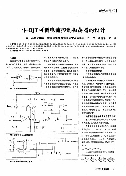
本文 所 设计 的振 荡器 电路 结构 主要 分 为 两 部分 :充 电 电路 和放 电电路 。
充电电路示意图如图2 所示 ,运算放
大 器A与R ,R ,R ,RI 1 2 3 0 1 2 4 。,Q ,Q ,Q 组 t
… … … … … … … … … … … … … … … … … … _ _ … … … … … J
外接 电阻大小,调节电容 充电电流大小,使振 荡器频 率可 以连续调节 。通过使 用 ̄ ̄l m 5vBT u J 工艺库进行 了仿真 ,验证 了振荡器频率在3k z 3 k z 6 5 H ~1 5H 内可调, 使 振荡频率受温度 、电源电压以及 工艺偏 差的影响降低 。
【 关键词 】双极工艺;振荡器;电容充放电;频率可调
成 了一个 带 负 反馈 环路 的 运算 放 大器 ,将 f e 端 得 电压 钳 位 至V ,Ve 电压 为 一 rq r端 f
图2振 荡 器充 电 电路示 意图
r ’ ’ ’ 。 。 。 。 ‘ 。 ‘ ’ ’ ’ ’ 。 。 。 。 ‘ ‘ 。 ‘ 一 ● ’ ’ 。 。 。 ‘ ‘ ‘ - ’ 一 。 。 - ‘ - ‘ 。 ‘ 。 。 。 ‘ 。 ‘ ‘ ● ’ ’ 。 。 。 ‘ 。 ’ ’ 。 。 。 。 ‘ 。 - ’ ‘ ’
…
…
…
…
…
…
………… Nhomakorabea.
鳗 廑 . -
一
种B T J 可调 电流控制振荡器的设计
电子科技大学 电子薄膜与集成器件 国家重点实验室 代 杰 余清华 宋 健
【 摘要 】提出了一 种基于 双极工艺的 低成 本振荡 器电 路结构, 该振荡 器电 路利用系统内 部参考电压 和外 接电阻产生的电流 信号 对电 客进行充放电, 通过调 节
FAB名词

1 Active Area 主动区(工作区)主动晶体管(ACTIVE TRANSISTOR)被制造的区域即所谓的主动区(ACTIVE AREA)。
在标准之MOS制造过程中ACTIVE AREA是由一层氮化硅光罩即等接氮化硅蚀刻之后的局部场区氧化所形成的,而由于利用到局部场氧化之步骤,所以ACTIVE AREA会受到鸟嘴(BIRD’S BEAK)之影响而比原先之氮化硅光罩所定义的区域来的小,以长0.6UM之场区氧化而言,大概会有0.5UM之BIRD’S BEAK 存在,也就是说ACTIVE AREA比原在之氮化硅光罩所定义的区域小0.5UM。
2 ACTONE 丙酮 1. 丙酮是有机溶剂的一种,分子式为CH3COCH3。
2. 性质为无色,具刺激性及薄荷臭味之液体。
3. 在FAB内之用途,主要在于黄光室内正光阻之清洗、擦拭。
4. 对神经中枢具中度麻醉性,对皮肤黏膜具轻微毒性,长期接触会引起皮肤炎,吸入过量之丙酮蒸汽会刺激鼻、眼结膜及咽喉黏膜,甚至引起头痛、恶心、呕吐、目眩、意识不明等。
5. 允许浓度1000PPM。
3 ADI 显影后检查 1.定义:After Developing Inspection 之缩写2.目的:检查黄光室制程;光阻覆盖→对准→曝光→显影。
发现缺点后,如覆盖不良、显影不良…等即予修改,以维护产品良率、品质。
3.方法:利用目检、显微镜为之。
4 AEI 蚀刻后检查 1. 定义:AEI即After Etching Inspection,在蚀刻制程光阻去除前及光阻去除后,分别对产品实施全检或抽样检查。
2.目的:2-1提高产品良率,避免不良品外流。
2-2达到品质的一致性和制程之重复性。
2-3显示制程能力之指针2-4阻止异常扩大,节省成本3.通常AEI检查出来之不良品,非必要时很少作修改,因为重去氧化层或重长氧化层可能造成组件特性改变可靠性变差、缺点密度增加,生产成本增高,以及良率降低之缺点。
FA3641
58s Dimensions, mmSOP-8~85DIP-80˚5s DescriptionThe FA3641P(N) and FA3647P(N) are the PWM type switching power supply control ICs that can directly drive power MOSFET. These ICs use a CMOS device with high dielectric strength (30V) to implement low power consumption. They feature a number of functions that are equivalent to those of the FA531X series consisting of bipolar devices. In addition, they have a function that reduces the oscillation frequency to suppress loss of the power supply in light load mode and support an overvoltage protection detecting Vcc voltage. These ICs are most suitable for high-performance, energy-saving power supplies that require low input power in standby or no-load mode.s Features•Uses a newly developed CMOS process with high dielectric strength (30V) for implementing low power consumption •Standby current of 2µA or less (at Vcc=14V), and operating current of 1.9mA (typ.)•Automatically reduces the oscillation frequency to suppress loss of the power supply in light load mode•Overvoltage protection function detecting Vcc voltage• A drive circuit for connecting a power MOSFET directly •Output peak current:Source current–500mASink current +1A•Pulse-by-pulse overcurrent limiting function•Overload cutoff function (latch or non-latch mode selectable)•Output ON/OFF control function by external signal•Latch mode overvoltage shutdown function •Undervoltage lockout function(16.5V ON / 9V OFF)•Reference voltage output (5V)•8-pin package (DIP/SOP)FA3641P(N), FA3647P(N)59s Absolute maximum ratings (T a=25˚C)I temSymbol Test conditionRating Unit Supply voltage V CC 1Low impedance source (Icc >15mA)30V V CC 2Internal ZD clamp (Icc < 15mA)Self limiting V Output peak current I OL Sink current +1.0A I OH Source current–0.5A FB pin input voltage V FB –0.3 to 5.0V REF pin output current I REF –10mA IS pin input voltage V IS –0.3 to 5.0V CS pin input current I CS 2.0mA T otal power dissipation P d at T a =25˚CDIP 800 *1mW SOP400 *2Operating temperature T opr –30 to +85˚C Junction temperature T j 125˚C Storage temperatureT stg–40 to +150˚Cs Block diagram FA3641FA3647Note:*1Derating factor T a > 25˚C: 8.0mW/˚C Maximum power dissipation curve* 2 Derating factor Ta > 25˚C: 4.0mW/˚C–3025851250Ambient temperature T a [˚C]M a x p o w e r d i s s p a t i o n400mW (SOP)800mW (DIP)Pin No.Symbol Function Description1RT Oscillator timing Setting oscillation frequency resistor 2FB Feedback Input to PWM comparator 3IS (+)/Overcurrent Input to overcurrent limiting IS (–)detection function 4GND Ground Ground5OUT Output Output for direct driving a power MOSFET 6VCC Power supplyPower supply for IC 7REF Reference voltage Reference voltage output (5V)8CSSoft-start and Soft-start, ON/OFF and latch-ON/OFF controlmode shutdown operationsFA3641P(N), FA3647P(N)s Recommended operating conditionItem Symbol Min.Typ.Max.UnitSupply voltage V CC1028VREF pin bypass capacitor C ref0.10.47µFSoft-start capacitor C S0.011µF Oscillation frequency (FB >1.2V)f OSC30500kHzMin.oscillation frequency at light load mode (FB <1.2V)f OSCL10kHzs Electrical characteristics (Vcc=18V, R T=47kΩ, Ta=25˚C)Reference voltage sectionItem Symbol Test condition Min.Typ.Max.Unit Reference voltage VREF Tj=25˚C 4.75 5.00 5.25V Voltage variation 1 (Line regulation)V dV V CC=10 to 28V±6±20mV Voltage variation 2 (Load regulation))V dV I L=0 to 10mA, V cc=18V±6±20mV Voltage variation 3 (Temperature stability)V dT Ta= –30 to +85°C±0.5mV/°COscillator sectionItem Symbol Test condition Min.Typ.Max.Unit Oscillation frequency f OSC R T=47kΩ, Tj=25˚C92.6100107.4kHz Frequency variation 1 (Voltage stability)f dV V CC=10 to 28V±1.6% Frequency variation 2 (Temperature stability)f dT Ta= –30 to +85°C±0.02% / °CPulse width modulation circuit sectionItem Symbol Test condition Min.Typ.Max.Unit FB pin source current I FB V FB=0V–985–750–615µA Input threshold voltage (FB pin)V TH FBO Duty cycle =0%0.95 1.03VV TH FBM Duty cycle =D MAX 2.40V Maximum duty cycle D MAX V FB=2.5V667074%Reducing oscillation frequency sectionItem Symbol Test condition Min.Typ.Max.Unit FB pin threshold voltage V TH FBS 1.18V Frequency reduction k f S1V FB=1.10 to 1.15V16.7kHZ Minimum oscillation frequency f osc S246kHZOvercurrent limiting circuit sectionItem Symbol Test condition FA3641P/N FA3647P/N UnitMin.Typ.Max.Min.Typ.Max.Input threshold voltage (IS pin)V TH IS215235255–188–168–148mV Input terminal source current (IS pin)I IS V IS =0V–5–20µA Delay time T PD IS150150nsSoft-start circuit sectionItem Symbol Test condition Min.Typ.Max.Unit Charge current (CS pin)I CHG V CS =1V, Tj=25˚C–4.0–6.5–9.0µA Input threshold voltage (CS pin)V TH CSO Duty cycle =0%0.95 1.03VV TH CSM Duty cycle =D MAX 2.40V60FA3641P(N), FA3647P(N)Output ON/OFF circuit sectionItem Symbol Test condition Min.Typ.Max.UnitCS pinl source current I socs V CS=0V, Tj=25˚C–4.0–6.5–9.0µAOFF-to-ON threshold voltage (CS pin)V TH ON OFF→ON, Tj=25˚C0.820.95VON-to-OFF threshold voltage (CS pin)V TH OFF ON→OFF, Tj=25˚C0.500.68V Latch-mode cutoff circuit sectionItem Symbol Test condition Min.Typ.Max.UnitCS pin sink current I SICS V CS=6.5V, V FB=1V, Tj=25˚C203550µA Cutoff threshold voltage (CS pin)V TH CSF ON→OFF, Tj=25˚C8.08.59.0VV TH CSN OFF→ON, Tj=25˚C7.47.98.4V Hysteresis V TH HIS0.6VOverload cutoff circuit sectionItem Symbol Test condition Min.Typ.Max.Unit Cutoff threshold voltage (FB pin)V TH FB 2.8 3.0 3.3VOvervoltage cutoff circuit sectionItem Symbol Test condition Min.Typ.Max.Unit Cutoff threshold voltage (Vcc pin)V TH VCC Tj=25˚C303234VCutoff operating supply current (Vcc pin)I VCC Tj=25˚C13mA Charge current (CS pin)I SO CS2V CS=6.5V–0.5–0.9–1.4mAUndervoltage lockout circuit sectionItem Symbol Test condition Min.Typ.Max.Unit OFF-to-ON threshold voltage V CC ON Tj=25˚C15.516.517.5VON-to-OFF threshold voltage V CC OFF Tj=25˚C8.59.010.0V Hysteresis V HYS Tj=25˚C 6.87.58.2VOutput sectionItem Symbol Test condition Min.Typ.Max.UnitL-level output Voltage V OL I O=100mA0.7 1.5VH-level output Voltage V OH I O= –100mA, V CC=18V1516.5VRise time tr OUT=1000pF50nsFall time tf OUT=1000pF40ns Overall deviceItem Symbol Test condition Min.Typ.Max.Unit Standby current I CC STB V CC=14V2µA Startup current I CC ST V CC=V CCON1230µA Operating-state supply current I CC OP No load 1.9 2.5mA OFF-state supply current I CCOF V CC=17V, Cs=0V100µA Cutoff-state supply current I CCL V CC=10V45100µA61FA3641P(N), FA3647P(N)62s Characteristic curves (T a=25˚C)Oscillation frequency (fosc) vs.Oscillation frequency (fosc) vs. supply voltage (Vcc)timing resistor resistance (R T )Oscillation frequency (fosc) vs.L-level output vltage (V OL) vs. supply voltage (Vcc)junction temperature (Tj)Supply current (Icc) vs. supply voltage (Vcc)Supply current (Icc) vs. junction temperature (Tj)Operating modeOperating mode100101000f o s c [k H z ]Rt [k Ω]9697989910010510110210310495f o s c [k H z ]Vcc [V]989910010110210310497105f o s c [k H z ]Tj [°C]0.20.40.60.810V O L [V ]Vcc [V]1.81.851.91.9521.75I c c [m A ]Vcc [V]1.81.851.91.9521.75I c c [m A ]Tj [°C]FA3641P(N), FA3647P(N)63Supply current (Icc) vs. supply voltage (Vcc)Supply current (Icc) vs. supply voltage (Vcc)Latch modeLatch modeSupply current (Icc) vs. supply voltage (Vcc)Supply current (Icc) vs. supply voltage (Vcc)OFF modeOFF modeUVLO OFF-to-ON thrreshold voltage (Vcc on) vs.UVLO ON-to-OFF thrreshold voltage (Vcc off) vs.junction temperature (Tj)junction temperature (Tj)1210141640801201602000I c c [µA ]Vcc [V]18201510202550010001500200025000I c c [µA ]Vcc [V]3030001210141640801201602000I c c [µA ]Vcc [V]18201510202550010001500200025000I c c [µA ]Vcc [V]303000–505010016.216.416.616.81.716V c c o n [V ]Tj [°C]1500–50501008.999.19.28.8V c c o f f [V ]Tj [°C]150FA3641P(N), FA3647P(N)64CS terminal current (Ics) vs. CS terminal voltage (Vcs)CS terminal current (Ics) vs. CS terminal voltage (Vcs)CS terminal charge current (Ichg) vs.FB terminal source current (I FB ) vs.junction temperature (Tj)FB terminal voltag (V FB )IS (+) terminal current (I IS (+)) vs.IS (–) terminal current (I IS (–)) vs.IS (+) terminal voltage (V IS (+))IS (–) terminal voltage (V IS (–))FA3641FA3647–5051015–10I c s [µA ]Vcs [V]2010203040–10I c s [µA ]Vcs [V]50–5050100–9–8–7–6–5–10I c h g [µA ]Tj [°C]150Vcc =18V CS = 0V1023–700–600–500–400–300–800I F B [µA ]V FB [V]4–2005–10000.501 1.5–0.3–0.2–0.1–0.4I I S (+) [µA ]V IS (+) [V]2 2.530–0.510.5 1.5–20–15–10–5–25I I S (–) [µA ]V IS (–) [V]252.53FA3641P(N), FA3647P(N)65Fig. 1 OscillatorFig. 2 Oscillator outputFig. 3 Oscillation frequencys Description of each circuit1. OscillatorThe oscillator generates a triangular waveform by charging and discharging the built-in capacitor. A desired oscillationfrequency can be set by the value of the resistor connected to the RT pin (See Figure 1).The built-in capacitor voltage oscillates between about 3V and 1V , with almost the same charging and discharging gradients (Figure 2). Y ou can set the desired oscillation frequency by changing the gradients using the resistor connected to the RT pin. (Large Rt = low frequency, small Rt = high frequency) The oscillation frequency is automatically lowered when output duty cycle is small (FB Ϲ about 1.18V) in light load mode. For more information, see item 2, “Reducing oscillation frequency circuit in light-load mode.”The relationship between Rt and the fixed oscillation frequency is approximately given by: (1) (2)f O :Fixed frequency [kHz]Rt:Timing resistance [k Ω]The oscillator waveform cannot be observed from the outside because a pin for this purpose is not provided.The oscillator output is connected to a PWM comparator.The RT pin is 2.5V DC in normal fixed frequency operation mode. When the frequency is lowered, the voltage also decreases linearly to about 1V .2. Reducing oscillation frequency circuit in light-load mode To reduce the loss of the power supply in standby mode, this IC has a feature that automatically lowers the oscillationfrequency when the load is light. When the load is light, with the result that the IC output pulse width narrows below about 10% and the FB pin voltage decreases below about 1.18V,the oscillation frequency begins to decreases linearly until the output pulse width becomes 0. When the output pulse width is 0, the oscillation frequency is about 46% of normal fixed frequency (Figure 3). Even while the oscillation frequency is decreasing, the built-in capacitor voltage oscillates between about 3V and 1V .The frequency reduction rate (46%) can be adjusted from the outside. (See “Design advice ” for more information.)3. PWM comparatorThe PWM comparator has four inputs as shown in Figure 4.Oscillator output ቢ is compared with CS pin voltage ባ, FB pin voltage ቤ, and DT voltage ብ. The lowest of three inputs ባ, ቤ, and ብ has priority and is compared with output ቢ.While the voltage is lower than the oscillator output, the comparator output is high. While the voltage is higher than the oscillator output, the PWM comparator output is low (see Figure 5). The IC OUT pin voltage is high while the PWM comparator output is low.When the IC is powered up, CS pin voltage ባ controls soft start operation. The output pulse then begins to widengradually. During normal operation, the output pulse width is determined within the maximum duty cycle (70%) set by DT voltage ብ under the condition set by FB pin voltage ቤ, to stabilize the output voltage.Fig. 4 PWM comparatorFig. 5 PWM comparator timing chartRt [k Ω] Լ 4880– 1.4f 0f 0 [kHz] Լ 4880Rt + 1.4FA3641P(N), FA3647P(N)66Fig. 7 CS pin waveformFig. 6 CS pin circuit4. CS pin circuitAs shown in Figure 6, capacitor Cs is connected to the CS pin.The CS pin voltage varies depending on the charging voltage of this capacitor Cs. When the power is turned on, the constant current source (6.5µA) begins to charge capacitor. Accordingly,the CS pin voltage rises as shown in Figure 7. The CS pin voltage is connected to the PWM comparator, which is characterized to make output based on the lowest of input voltages. The device enters soft-start mode while the CS pin voltage is between 1.0V and 2.4V . During normal operation, the CS pin is clamped at 4.0V by internal zener diode.If the output voltage drops due to an overload and the FBvoltage rises to 3V or more, the clamp voltage 4.0V is canceled and the CS pin voltage rises to 9.5V . The CS pin is alsoconnected to latch comparator C2. If the CS pin voltage rises to 8.5V or more, comparator C2 toggles to turn off the 5V REF circuit, thereby shutting the output down. Since the CS pin is also connected to comparator C1, the 5V REF circuit can be turned off to shut the output down by dropping the CS pin voltage below 0.68V . In this way, comparator C1 can be used for output on-off control.As explained above, the CS pin can be used for soft-start,overload output shutdown, and output on-off control by varying the voltage.Further details on the above three major functions of the CS pin are given below.4.1Soft start functionFigure 8 shows the soft start circuit. Figure 9 is a soft-start operation timing chart. The CS pin is connected to capacitor Cs. When the power is turned on, the constant current source (6.5µA) begins to charge the capacitor. As shown in the timing chart, the CS pin voltage rises slowly in accordance with the capacitor Cs charging current. The CS pin is also connected to the IC internal PWM comparator, which has suchcharacteristics that the voltage is determined to output on the basis of the lowest of input voltages. The comparator output pulse slowly widens to cause a soft start as shown in the timing chart.The soft start period can be approximately estimated by the period t S , from the time the IC is activated to the time the output pulse width widens to 30%. The period is given by the following equation:ts [ms] Լ 250 ϫ Cs (3)Cs : Soft start capacitor [µF]Fig. 8 Soft-sart circuitFig. 9 Soft-sart timing chartFA3641P(N), FA3647P(N)67Fig. 10 Overload shutdown circuit4.2 Overload shutdown functionFigure 10 shows the overload shutdown circuit, and Figure 11is a timing chart that illustrates overload shutdown operation.If the output voltage drops due to an overload or short circuit,the FB pin output voltage rises. If the FB pin voltage exceeds the reference voltage (3.0V) of comparator C3, the output of comparator C3 goes low to turn off the switch. With the switch off, the CS pin voltage clamped at 4.0V by zener diode in normal operation is unclamped, and the constant currentsource (6.5µA) begins to charge capacitor Cs again and the CS pin voltage rises. When the CS pin voltage exceeds the reference voltage (8.5V) of comparator C2, the output of comparator C2 toggles to turn off the 5V REF circuit. The IC then enters the latched mode and shuts down the output. IC current consumption for shutdown is 45µA (typ) (Vcc = 10V).This current must be supplied through the startup resistor. The IC enters output off (low voltage) state.The overload shutdown operation can be reset by lowering the supply voltage Vcc to below the OFF threshold voltage (9.0V)or forcing the CS pin voltage below 7.9V .The period t OL from the time the output is short-circuited to the time the output circuit goes off is given by the following equation:t OL [ms] Լ 690 ϫ Cs (4)Cs: Soft start capacitor [µF]When you want to disable the overload shutdown function, see item 11 in “Design advice ”4.3Output ON/OFF control functionThe IC can be turned on or off via an external signal applied to the CS pin. Figure 12 shows the output on/off control circuit,and Figure 13 is a timing chart.The IC is turned off when the CS pin voltage is externally made to drop below 0.68V (typ). The output of comparator C1 goes high to turn the 5V REF circuit. This shuts the output down.The IC enters output off (low voltage) state. Required IC current consumption during shutdown is 100µA (typ) (Vcc =17V). This current must be supplied through the startup resistor. The IC goes on when the CS pin is opened and the CS pin voltage exceeds 0.82V (typ). This turns on the 5V REF circuit and results in automatic soft start. The power supply then restarts operation.Fig. 11 Overload shutdown timing chartFig. 12 External output ON/OFF control circuitFA3641P(N), FA3647P(N)68Fig. 14 Overcurrent limiting circuitFig. 15 Overcurrent timing chartFig. 17 Overvoltage shutdown timing chartFig. 16 Overvoltage shutdown circuit 5. Overcurrent limiting circuitThe overcurrent limiting circuit detects the peak value of every drain current pulse (pulse by pulse method) of the main switching MOSFET to limit the overcurrent. The detectionthreshold voltage is +0.235V for FA3641 or –0.168V for FA3647with respect to the ground as shown in Figure 14.The drain current of the MOSFET is converted to voltage by resistor Rs and fed to the IS pin of the IC. If the voltageexceeds the reference voltage +0.235V (FA3641) or –0.168V (FA3647) of comparator C4, comparator C4 works to set flip-flop output Q to high. The output is immediately turned off to shut off the current. Flip-flop output Q is reset on the next cycle to turn on the output again. This operation is repeated to limit the overcurrent.If the overcurrent limiting circuit malfunctions due to noise,place an RC filter between the IS pin and MOSFET as shown in Figure 14. (See item 14 in “Design advice.”)Figure 15 is a timing chart that illustrates overcurrent-limiting operations.6. Vcc overvoltage protection circuitThe IC contains a Vcc overvoltage protection circuit to protect the IC from damage by overvoltage. Figure 16 shows the overvoltage protection circuit. Figure 17 is a timing chart that illustrates overvoltage protection operations.Overvoltage is detected if the supply voltage Vcc rises to 32V (Icc = 13mA) or more and current flows in the built-in zener diode. The output of comparator C5 then goes high and the constant current source (0.9mA) raises the CS pin voltage.When the CS pin voltage exceeds 8.5V , the output ofcomparator C2 goes high to turn off the 5V REF circuit. The IC then enters the latched mode and the IC output is put in the off (low voltage) state. When latched mode, the IC currentconsumption is 45µA (typ) (Vcc = 10V). This current must be supplied through the startup resistor.The overvoltage shutdown operation can be reset by lowering the supply voltage to below 9.0V or forcing the CS pin voltage below 7.9V .(When you want to enable Vcc overvoltage shutdown at a desired voltage, see item 7 in “Design advice.”FA3641P(N), FA3647P(N)69Fig. 18 Oscillator circuitRr [k Ω] Լ2.35A – Bf 0 [kHz] Լ 4880 RtRr + 1.4 Rr – Rt fr [kHz] Լ2500RtRr+ 6Rr – 3.35RtA =f 00 B =f r 2500 – 6f rFA3641P(N), FA3647P(N)70Fig. 19 Startup circuit (1)Fig. 20 Startup circuit (2)2. Deciding the startup circuitThese ICs, which use CMOS process, consume less current,and therefore can use larger startup resistance than the conventional bipolar type of IC.T o decide the startup resistance, the following conditions must be satisfied:(a) The IC is started when the power is turned on.(b)The IC consumption current is supplied during latchmode operation to maintain the latch state.(c)The IC consumption current is supplied during the off stateunder the on/off function to maintain the off state.However, these are the minimum conditions for using the IC.The startup time required for the power supply must also be decided on.2.1Connecting a startup resistor before rectification(AC line)When the startup resistor is connected before rectification (AC line) as shown in Figure 19, the voltage applied to the startup resistor forms a half-wave rectified waveform of the AC input voltage.Startup resistor R1 must satisfy the three equations shownbelow. Select a smaller-side value for R1 in consideration of the temperature characteristics.(a)T o supply startup current 30µA at ON threshold voltage17.5V (max.) of UVLO: (8)(b)T o supply IC consumption current 100µA (max.) (Vcc =10V)in latch mode: (9)(c)T o supply IC consumption current 200µA (max.) (Vcc =17V)in the off state under the on/off function: (10)R1:Startup resistance [k Ω]Vac:Effective value of AC input voltage [V]If neither the latch mode operation nor the on/off functions are used, only the expression in (8) needs to be satisfied.In this method, the supply current to the IC via the start-upresistor is stopped when AC input is shut down. Therefore, after latch mode operation, shutting the AC input down resets the latch mode in a very short period of time.2.2Connecting the startup resistor after rectification(DC line)When the startup resistor is connected after rectification (DC line) as shown in Figure 20, the voltage applied to the startup resistor becomes the peak value of the AC input voltage.Startup resistor R1 must satisfy the three equations shown below. Select a smaller-side value for R1 in consideration of temperature characteristics.(a)T o supply startup current 30µA at ON threshold voltage17.5V (max.) of UVLO: (11)R1 [k ΩR1 [k Ω 2؋ Vac – 17.5R1 [k Ω] < πFA3641P(N), FA3647P(N)71Fig. 21 Vcc voltage at startup with an adequate capacitorFig. 22 Vcc voltage at startup with an inadequate capacitorFig. 23 Startup circuit (3)(b)T o supply IC consumption current 100µA (max.) (Vcc =10V)in latch mode: (12)(c)T o supply IC consumption current 200µA (max.) (Vcc = 17V)in the off state under the on/off function: (13)R1:Startup resistance [k Ω]Vac:Effective value of AC input voltage [V]If neither the latch nor the on/off functions are used, only the expression in (11) needs to be satisfied.In this method, after latch mode operation, smoothing capacitor C1 in the main circuit supplies current to the IC via the startup resistor even if the AC input is shut down. Therefore, some time must elapse before the latch mode is reset.3. Determining the Vcc capacitor valueT o properly start the power supply, a certain value is required for the capacitor connected to the VCC pin.Figure 21 shows the Vcc voltage at start-up when a proper value is given to the capacitor.When the input power is turned on, the capacitor connected to the VCC pin is charged via the startup resistor and the voltage increases. The IC is then in standby state and almost no current is consumed. (Icc < 2µA)Thereafter, Vcc reaches the ON threshold voltage of UVLO and the IC begins operation.When the IC begins operation to make output, the IC operates based on the voltage from the auxiliary winding. When the IC is just starting up, however, it takes time for the voltage from the auxiliary winding to rise enough, and Vcc drops during this period.Determine the Vcc capacitor value so that Vcc will not drop down to the OFF threshold voltage of UVLO during this period.If the Vcc capacitor value is too small, Vcc will drop to the OFF threshold voltage of UVLO before the auxiliary winding voltage rises enugh. If so, Vcc repeatedly goes up and down between the UVLO threshold voltages, and the power supply cannot start up. (Figure 22)4. Shortening the startup periodIncreasing the resistance of the startup resistor to reduce loss prolongs the startup period. Figure 23 shows a circuit for shortening the startup period. The C2 capacitance isdecreased to shorten the startup period and, after the IC starts up, power is supplied from C3.5. Setting soft start period and OFF latch delay independently Figure 24 shows a circuit for setting the soft start period and OFF latch delay independently. In this circuit, capacitance CS determines the soft start period, and capacitance CL determines the OFF latch delay.If the overload shutdown or overvoltage shutdown functions raise the CS pin voltage to around 5V , zener diode Zn becomes conductive to charge capacitor CL. The OFF latch delay can be thus prolonged by capacitance CL.Fig. 24Independent setting of soft start period andOFF latch delayWhen the capacitor value is adequateWhen the capacitor value is inadequateR1 [k ΩFA3641P(N), FA3647P(N)726. Overvoltage protection using the VCC pinThese ICs contain an overvoltage protection function detecting the Vcc voltage using internal ZD (See item 6 in “Description of each circuit ”). If Vcc voltage exceed about 32V , the current of 13mA flows through the internal ZD and the overvoltage protection function operates.After this protection function operates, the IC continues to consume the large current if high voltage continues to beapplied to the Vcc pin. Mind that total IC loss does not exceed the rating.If the voltage source applied to Vcc pin has relatively highimpedance and cannot supply the current of 13mA, overvoltage protection function does not operate. But the internal ZD maintains the Vcc voltage 32V or less and protects the IC.7. Overvoltage protection using CS pinThese ICs contain the overvoltage protection function detecting Vcc voltage. However, the threshold voltage is fixed. Adding a circuit to CS pin enables the overvoltage protection detecting desired voltage.7.1 Detecting on secondary sideFigure 25 shows the overvoltage shutdown circuit based on the signal from the secondary side. The optocoupler outputtransistor is connected between the CS and Vcc pins. When the output voltage is put in the overvoltage state, the optocoupler output transistor goes on to raise the CS pinvoltage via resistor R2. When the CS pin voltage exceeds the reference voltage (8.5V) of comparator C2, the output of the comparator C2 goes high to turn off the 5V REF circuit.Accordingly, the IC enters the OFF latch mode and shuts the output down. The IC consumes current 45µA (typ) (Vcc = 10V)in latch mode. This current must be supplied via startup resistor R1.The overvoltage protection circuit can be reset by lowering the supply voltage Vcc to below 9.0V or forcing the CS pin voltage below 7.9V .In normal operation, the CS pin voltage is clamped by the 4V zener diode with maximum sink current 50µA . Therefore, to raise the CS pin voltage to 8.5V or more, 50µA or a higher current needs to be supplied from the optocoupler. Set the current input to the CS pin to 1mA or less.7.2 Detecting on primary side (detecting Vcc voltage)T o attain overvoltage protection, the CS pin voltage is forcibly raised from outside the IC until it exceeds the reference voltage (8.5V) of the internal comparator C2. When the reference voltage is exceeded, the IC enters latch mode and shuts the output down. Connect a zener diode (ZD) and resistor between the Vcc and CS pins as shown in Figure 26. When the Vcc voltage exceeds about ZD voltage + 8.5V , the ICs enter the OFF latch mode and shut the output down. If Vcc remains high even after shutdown and current is input to the CS pin, set the current to 1mA or lower.Set the zener voltage of the ZD connected to the CS pin higher than the UVLO ON threshold voltage. Startup is disabled below this voltage.Figure 27 shows another circuit for enabling latch modeshutdown by detecting a desired Vcc voltage using the CS pin.In this circuit, overvoltage shutdown works when the Vcc voltage is about the same as the ZD voltage.For this circuit also, use a ZD voltage higher than the UVLO ON threshold voltage. Set the current flowing into the CS pin to 1mA or lower.Fig. 25 Overvoltage shutdown circuit (1)Fig. 26 Overvoltage shutdown circuit (2)Fig. 27 Overvoltage shutdown circuit (3)。
- 1、下载文档前请自行甄别文档内容的完整性,平台不提供额外的编辑、内容补充、找答案等附加服务。
- 2、"仅部分预览"的文档,不可在线预览部分如存在完整性等问题,可反馈申请退款(可完整预览的文档不适用该条件!)。
- 3、如文档侵犯您的权益,请联系客服反馈,我们会尽快为您处理(人工客服工作时间:9:00-18:30)。
Current-Ratio Temperature Compensation in Bipolar Relaxation OscillatorsM.H. Splithof1, A.J.M. van Tuijl1, S.L.J. Gierkink2, E.A.M. Klumperink21Philips Semiconductors, Nijmegen, The Netherlands
2MESA Research Institute, University of Twente, Enschede, The Netherlands
Mike.Splithof@nym.sc.philips.com, Ed.vanTuijl@nym.sc.philips.comS.L.J.Gierkink@el.utwente.nl, E.A.M.Klumperink@el.utwente.nl
AbstractA new temperature compensation strategy forbipolar relaxation oscillators is presented. Thecompensation scheme is suitable for both Schmitt-trigger oscillators and emitter-coupled multivibratorsand requires a minimum amount of circuitry for thecompensation. The feasibility of this compensationscheme is demonstrated by the results of a test chip.Without any trimming and with a total currentconsumption of 2.5mA, a temperature coefficient ofapproximately -90ppm/°C has been achieved at
frequencies up to 2.5MHz.
1.IntroductionBipolar relaxation oscillators are frequently used inmonolithic voltage controlled oscillator designs. Theseoscillators display excellent control linearity, thoughtemperature compensation has always been animportant issue. Among the bipolar relaxationoscillators, two major subclasses can be distinguished,which are formed by Schmitt-trigger oscillators andmultivibrators. Various temperature compensationtechniques have been reported [1],[2], though theseschemes always focus on either Schmitt-triggeroscillators or multivibrators.The current-ratio temperature compensation strategy,which will be presented in this paper, offers goodperspectives for both Schmitt-trigger oscillators andmultivibrators. The key in the approach is the fact thatthe currents in all branches of the oscillator core aredefined by the circuit topology only. Utilisingtranslinear loops, the hysteresis voltage is then definedby a precise reference voltage, thereby eliminating thefundamental origin of temperature dependence.
2.Temperature compensation inSchmitt-trigger oscillators
2.1.Schmitt-trigger oscillatorsA well-known bipolar Schmitt-trigger oscillator is
depicted in Figure 1. Its operation is briefly explained asfollows. At any time, either T1 or T2 is conducting,
causing the output voltage across the resistor R1 to be
either low or high. This output voltage controls acurrent switch such that the timing capacitor C is eithercharged or discharged, resulting in a triangular voltagewaveform across the timing capacitor. Due to thepositive feedback, the Schmitt-trigger circuit willremain in a stable state until a critical voltage level atthe trigger input is reached, at which time the circuitwill change state. Subsequently, the current switch willbe operated, such that the timing capacitor will bealternately charged and discharged by a current IC, the
frequency of oscillation being defined by the controlcurrent IC, the capacitor C and the hysteresis voltage of
the Schmitt-trigger.
Schmitt-trigger
+_I0
VIN
+VCC
R1
T2T1
+
_VOUT
IC
2ICC
Figure 1. Basic Schmitt-trigger oscillatorThe hysteresis voltage of the bipolar Schmitt-triggerstrongly depends on temperature [1], which implies thatthe frequency of oscillation has to be compensated fortemperature dependence.
2.2.The current-ratio Schmitt-triggerThe current-ratio Schmitt-trigger [3] is based uponthe basic bipolar Schmitt-trigger and is shown in Figure2. In this circuit, temperature compensation of thehysteresis voltage is achieved by an adaptation of thecircuit topology. T1 and T2 can be recognised to be a
differential pair with unity gain positive feedback. Theresistive collector load of the bipolar Schmitt-trigger has
利用电路的延迟been replaced by a VLO-cell, composed of T5 through T8,and a VHI-cell, which consists of T3 and T4.+_+_2I02I02I0I0VHIVLOVIN+VCCVLO-cell+_VHI-cellI0T2T1T4T3T8T7T6T5VOUTFigure 2. The current-ratio Schmitt-triggerThe circuit operation will now be explained. First,suppose that VOUT is high. Since transistor T5 is off, thecollector load of transistor T1 equals the small signalimpedance of the VHI-cell.(1)4e3eHIrrZ+=Assume that T1 carries a current (1-λ)I0. Then, IC2,IC3 and IC4 can also be expressed in terms of I0 and λ:(2)01CI)1(I⋅λ−= 02CI)1(I⋅λ+=03CII⋅λ= 04CI)2(I⋅λ−=The regeneration process will start when the loop gainreaches unity. This occurs when the collector loadresistance equals the sum of the emitter load resistances:(3)4e3e2e1errrr+=+Assuming equal junction temperatures for alltransistors, substitution of the collector currents andsolving for the current ratio λ yields:(4)212111111HI=λ=λ⇒λ−+λ=λ++λ−After the Schmitt-trigger has changed state, thecollector load of T1 equals the small signal impedanceof the VLO-cell. Now, regenerative switching will occurwhen:(5)5e2e1errr=+Continuing the calculation yields the current ratio atthe lower switching instant: λLO= -1+√2.Summarising: the current ratios at the regenerationinstant are uniquely defined by the circuit topology andindependent of temperature or the absolute values of thecollector currents.Now, let us take a closer look at the circuit when theinput voltage VIN approaches VHI. A translinear loop canbe recognised from VIN to VHI.