PW2052 pdf降压芯片规格书

- 1、下载文档前请自行甄别文档内容的完整性,平台不提供额外的编辑、内容补充、找答案等附加服务。
- 2、"仅部分预览"的文档,不可在线预览部分如存在完整性等问题,可反馈申请退款(可完整预览的文档不适用该条件!)。
- 3、如文档侵犯您的权益,请联系客服反馈,我们会尽快为您处理(人工客服工作时间:9:00-18:30)。
PW2052
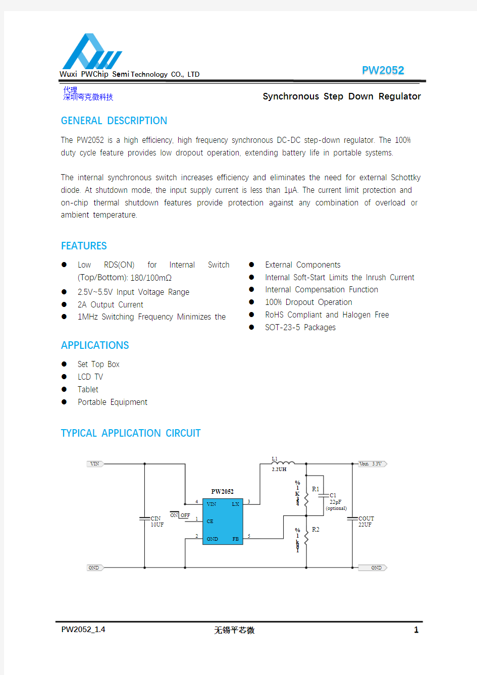
GENERAL DESCRIPTION
The PW2052 is a high efficiency, high frequency synchronous DC-DC step-down regulator. The 100% duty cycle feature provides low dropout operation, extending battery life in portable systems.
The internal synchronous switch increases efficiency and eliminates the need for external Schottky diode. At shutdown mode, the input supply current is less than 1µA. The current limit protection and on-chip thermal shutdown features provide protection against any combination of overload or ambient temperature.
FEATURES
● Low RDS(ON) for Internal Switch
(Top/Bottom): 180/100mΩ
● 2.5V~5.5V Input Voltage Range ● 2A Output Current
● 1MHz Switching Frequency Minimizes the
● External Components
● Internal Soft-Start Limits the Inrush Current ● Internal Compensation Function ● 100% Dropout Operation
● RoHS Compliant and Halogen Free ●
SOT-23-5 Packages
APPLICATIONS
● Set Top Box ● LCD TV ● Tablet
● Portable Equipment
TYPICAL APPLICATION CIRCUIT
深圳夸克微科技
The device’s performance and stability are dramatically affected by PCB layout. It is recommended to follow these general guidelines shown as below:
1. Place the input capacitors and output capacitors as close to the device as possible. The traces which connect to these capacitors should be as short and wide as possible to minimize parasitic inductance and resistance.
2. Place feedback resistors close to the FB pin.
3. Keep the sensitive signal (FB) away from the switching signal (LX).
4. Multi-layer PCB design is recommended.
Block Diagram
FB
GND
LX
●VIN to GND ---------------------------------------------- -0.3V to +6.5V
●LX to GND ----------------------------------------------- -0.3V to VIN+0.3V
●CE, FB, to GND ----------------------------------------- -0.3V to VIN
●Package Thermal esistance, (θJA)-- ------------------------ +250ºC/W
●Package Thermal esistance, (θJC) --------------------------- +130°C/W
●Maximum Junction Temperature (TJ) -------------------------- +150°C
●Lead Temperature (Soldering, 10 sec.) ------------------------- +260°C
●Storage Temperature (TSTG) --------------------------------- -65°C to +150℃
Note 1:Stresses beyond those listed under “Absolute Maximum atings" may cause permanent damage to the device
Recommended Operating Conditions (Note 2)
●Supply Voltage (VIN) ---------------------------------------- +2.5V to +5.5V
●Junction Temperature Range --------------------------------- -40°C to +125°C
●Ambient Temperature Range --------------------------------- -40°C to +85°C
Note 2:The device is not guaranteed to function outside its operating conditions.
