CdSe量子点的电荷存储

Organic bistable devices based on core/shell CdSe/ZnS nanoparticles embedded in a conducting poly …N -vinylcarbazole …polymer layer
Fushan Li,Dong-Ik Son,Seung-Mi Seo,Han-Moe Cha,Hyuk-Ju Kim,Bong-Jun Kim,Jae Hun Jung,and Tae Whan Kim a ?
Advanced Semiconductor Research Center,Division of Electronics and Computer Engineering,Hanyang University,17Haengdang-dong,Seongdong-gu,Seoul 133-791,Korea
?Received 16July 2007;accepted 16August 2007;published online 21September 2007?Current-voltage measurements on the Al/?CdSe/ZnS nanoparticles embedded in a hole-transporting poly ?N -vinylcarbazole ??PVK ?layer ?/indium tin oxide ?ITO ?/glass structures at 300K showed a nonvolatile electrical bistability behavior.Capacitance-voltage ?C -V ?measurements on the Al/?CdSe/ZnS nanoparticles embedded in a PVK layer ?/ITO/glass structures at 300K showed a metal-insulator-semiconductor behavior with a ?atband voltage shift due to the existence of the CdSe/ZnS nanoparticles,indicative of trapping,storing,and emission of charges in the electronic states of the CdSe nanoparticles.Operating mechanisms for the Al/?CdSe/ZnS nanoparticles embedded in the PVK layer ?/ITO/glass devices are described on the basis of the C -V results.?2007American Institute of Physics .?DOI:10.1063/1.2783189?
Organic structures containing inorganic nanoparticles have been particularly attractive due to interest in their prom-ising applications in electronic and optoelectronic devices 1–7because of their unique advantages of low-power consump-tion,high mechanical ?exibility,and chemical structural ver-satility.Such hybrid organic/inorganic devices are also excel-lent candidates for potential applications in next-generation transistor and memory devices.8,9Potential applications of memory devices utilizing nanoparticles embedded in organic layers have driven extensive effort to form various kinds of nanoparticles.10,11Even though some studies concerning the formation of metal nanoparticles embedded in an organic layer for applications such as nonvolatile organic bistable devices ?OBDs ?have been conducted,almost all of the devices were fabricated by using strin-gent high-vacuum evaporation method.12–14The memory effects of core/shell-type cadmium selenium ?CdSe ?nano-particles embedded in a conducting poly ?2-methoxy-5-?2-ethylhexyloxy ?-1,4-phenylene-vinylene ??MEH-PPV ?poly-mer fabricated by using a simple spin-coating technique were reported.15Because the narrow band gap of MEH-PPV leads to a low charge capturing ef?ciency,resulting in the realization of memory effect at a high bias voltage of 10V,a hole transport poly ?N -vinylcarbazole ??PVK ?matrix can be introduced here to obtain the memory effects in CdSe/PVK nanocomposites under an applied bias voltage as small as 2V.Furthermore,studies on the memory effects and their operating mechanisms for OBDs made of semiconductor nanoparticles embedded in a conducting polymer are very important for improving the ef?ciencies of nonvolatile ?ash memories.
This letter reports data for the bistability and the operat-ing mechanisms of the memory effects of OBDs fabricated utilizing CdSe semiconductor nanoparticles embedded in a PVK polymer layer.Core/shell-type CdSe nanoparticles have become particularly attractive because of their promising ap-plications in next-generation nonvolatile ?ash memory de-vices with low-power and ultrahigh-density elements.16,17Current-voltage ?I -V ?measurements were carried out to in-vestigate the electrical bistable properties of the fabricated OBDs containing CdSe/ZnS nanoparticles embedded in the PVK layer.Capacitance-voltage ?C -V ?measurements were carried out to investigate the possibility of fabricating memory effects involving the CdSe/ZnS nanoparticles em-bedded in the PVK layer.Furthermore,the dependence of the memory effects on the thickness of the PVK layer containing CdSe/ZnS nanoparticles was also investigated.
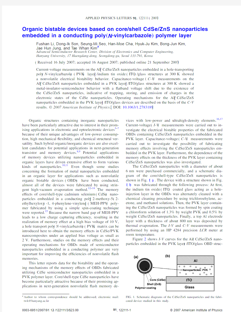
The CdSe/ZnS nanoparticles with a diameter of about 6nm were purchased commercially,and a schematic dia-gram of the core/shell-type CdSe/ZnS nanoparticles is shown in Fig.1?a ?.The device with a structure shown in Fig.1?b ?was fabricated through the following process:At ?rst,the indium tin oxide ?ITO ?coated glass acting as a hole-injection layer in the OBDs was alternately cleaned with a chemical cleaning procedure by using trichloroehylene,ac-etone,and methanol solutions.Then,the PVK layer contain-ing the CdSe/ZnS nanoparticles was formed by spin coating a chloroform solution of 1.3%by weight PVK and 0.5%by weight CdSe/ZnS nanoparticles.Finally,a top Al electrode layer with a thickness of about 800nm was deposited by thermal evaporation.The I -V and C -V measurements were performed by using an HP 4284precision LCR meter at room temperature.
Figure 2shows I -V curves for the Al/?CdSe/ZnS nano-particles embedded in the PVK layer ?/ITO/glass OBD struc-
a ?
Author to whom correspondence should be addressed;electronic mail:
twk@hanyang.ac.kr FIG.1.Schematic diagrams of the CdSe/ZnS nanoparticles and the fabri-cated device studied in this study.
APPLIED PHYSICS LETTERS 91,122111?2007?
0003-6951/2007/91?12?/122111/3/$23.00?2007American Institute of Physics 91,122111-1Downloaded 22 Oct 2007 to 166.104.58.178. Redistribution subject to AIP license or copyright, see https://www.360docs.net/doc/107892020.html,/apl/copyright.jsp
ture with a 500-nm-thick active layer.The I -V curve under a forward bias voltage,denoted by the empty rectangles in the lower curve of the Fig.2,shows a dramatic increase in the injection current at about 1V,indicative of a bistable tran-sition of the device from a low-conductivity state ?off state ?to a high-conductivity state ?on state ?.The bistable transition from the off state to the on state is equivalent to the “writing”process in a digital memory cell.18After that transition is ?nished,the on state remains in the device even after turning off the power,which is shown in the reverse bias voltage denoted by the ?lled rectangles in the upper curve of Fig.2.Figure 2clearly shows an electrical hysteresis behavior,which is an essential feature for bistable devices,and reveals the nonvolatile nature of the memory effect.19While the cur-rent difference between the on and off states for the PVK only device is negligible,the bistability in the Al/?CdSe/ZnS nanoparticles embedded in the PVK layer ?/ITO/glass device might be attributed to the screening of the applied electric ?eld due to the existence of the internal electric ?eld gener-ated by the captured charge carriers in the CdSe nanopar-ticles.The off state can be recovered by applying a reverse bias voltage.This is equivalent to the “erasing”process of a digital memory cell resulting from the discharge of CdSe nanoparticles.The solid line in Fig.2corresponds to the I -V curve of the device after the application of a ?2V bias and is almost identical to the I -V curve denoted by the empty square.The observation that the OBD device main-tains an on state at a reverse applied voltage is similar to those reported for an Al/2-amino-4,5-imidazoledicarbonitrile ?AIDCN ?organic/Al layer/AIDCN organic/Al system 18and an Al/AIDCN organic/Al nanoclusters/AIDCN organic/Al system.19
The C -V curves measured at 1MHz for the Al/?CdSe/ZnS nanoparticles embedded in the PVK layer ?/ITO/glass OBD structure are shown in Fig.3.The C -V curve shows a metal-insulator-semiconductor ?MIS ?behavior with charge trap regions,and the C -V behavior is similar to that of MIS memories with ?oating gates containing Si nanocrystals.20,21A clockwise hysteresis is clearly observed
in the C -V characteristics,indicative of the existence of sites occupied by charges.The presence of such sites is attributed to carrier charging and discharging in the CdSe/ZnS nano-particles.The ?atband voltage shift of the C -V curve for the OBDs with a relatively thinner hybrid layer of 500nm,which originates from charge accumulation and depletion due to variations in the applied voltage,is approximately 3V,as shown in Fig.2?a ?,which is enough to capture car-riers inside the nanoparticles.The C -V curve for samples without CdSe nanoparticles under identical measurement conditions showed no hysteresis.Therefore,the hysteresis appearing in Fig.2may be attributed to carriers trapped in the embedded CdSe/ZnS nanoparticles,a clear indication of the memory effect.21The ?atband voltage shift of the C -V curve decreases to approximately 1.5V with increasing thickness of the hybrid active layer to about 900nm,as shown in Fig.2?b ?.These results indicate that the ?atband voltage shift of the C -V curve related to the magnitude of the memory is signi?cantly affected by the thickness of the hy-brid active layer.
When a positive voltage is applied,after the injection of holes from the ITO into the highest occupied molecular or-bital ?HOMO ?level occurs through the Fowler-Nordheim tunneling process,the holes existing at the HOMO level are transported along the direction of the applied voltage through the hopping mechanism among the PVK molecules.22
An
FIG. 2.Current-voltage curves for the Al/?CdSe/ZnS nanoparticles embedded in a PVK layer ?/ITO/glass device.The scanning step of the applied voltage is 0.01V.Empty and ?lled rectangles represent the current-voltage curves of the forward and the reverse applied bias volt-ages,respectively.The solid line indicates the current-voltage curve after application of a reverse voltage pulse of ?2
V.
FIG. 3.Capacitance-voltage curves for the Al/?CdSe/ZnS nanoparticles embedded in PVK layer ?/ITO/glass devices with the active layer thicknesses of ?a ?500nm and ?b ?900nm.
Downloaded 22 Oct 2007 to 166.104.58.178. Redistribution subject to AIP license or copyright, see https://www.360docs.net/doc/107892020.html,/apl/copyright.jsp
intuitive proposal is that the holes actually encounter CdSe/ZnS nanoparticles which are traversing the sample,and with increasing electrical ?eld to a certain value,holes can tunnel through the ZnS shell into the valence band of the CdSe nanoparticles,as shown in Fig.4,resulting in the for-mation of an internal electric ?eld along the direction of the applied voltage.Because the capacitance of the device ex-hibits a larger decrease in comparison with the capacitance in the depletion layer formed in the ITO substrate under a posi-tive bias voltage,the C -V curve of the device shifts to the left,as shown in Fig.2.When a negative voltage is applied to the electrode,because the holes captured in the valence band of the CdSe nanoparticles under the negative electric ?eld are released into the PVK matrix and then transported to the ITO substrate,the erasing process is performed.Since the generated internal electric ?eld disappears due to the re-lease of the holes captured in the CdSe/ZnS nanoparticles,the C -V curve of the device shifts to the right,as shown in Fig.3.
Because the ?atband voltage shift for the Al/?CdSe/ZnS nanoparticles embedded in the PVK layer ?/ITO/glass device is signi?cantly affected by the thickness of the PVK layer containing CdSe nanoparticles,the magnitude of the memory effects can be moderately adjusted by varying the thickness of the active layer in the devices,which might be very im-portant for practical applications in memory devices.A simple mechanism for the dependence of the memory effects on the thickness of the PVK layer in which the CdSe/ZnS nanoparticles are embedded can be proposed.The probability of the charges being trapped by the CdSe/ZnS nanoparticles embedded in the PVK layer through the tunneling process is typically determined by the electric ?eld at the organic/inorganic interface.23A smaller number of the holes in the OBDs will be captured by the CdSe/ZnS nanoparticles due to the smaller electric ?eld resulting from an increase in thickness.Therefore,a smaller ?atband voltage shift is attrib-uted to a decrease in the internal electric ?eld generated by the trapped charges.
In summary,the bistability and the operating mecha-nisms of an organic/inorganic hybrid device consisting of CdSe/ZnS nanoparticles and a PVK composite were inves-tigated.The I -V curves at ambient temperature for the Al/?CdSe/ZnS nanoparticles embedded in the PVK layer ?/ITO/glass devices exhibited a nonvolatile electrical bistable be-havior.The C -V curve at room temperature for the Al/?CdSe/ZnS nanoparticles embedded in the PVK layer ?/ITO/glass capacitors showed a MIS behavior with a large ?atband voltage shift due to the existence of the CdSe/ZnS nanopar-ticles,indicative of trapping,storing,and emission of holes in the electronic states of the CdSe nanoparticles.The mag-nitude of the ?atband voltage shift was signi?cantly affected by the thickness of the PVK layer containing CdSe/ZnS nanoparticles,and a possible operating mechanism corre-sponding to the writing and erasing processes of memory devices was described on the basis of the C -V results.These results indicate that OBDs fabricated utilizing CdSe/ZnS nanoparticles embedded in PVK layers hold promise for po-tential applications in next-generation nonvolatile memories.This work was supported by the Korea Science and En-gineering Foundation ?KOSEF ?grant funded by the Korea government ?MOST ??No.R0A-2007-000-20044-0?.
1
H.Sirringhaus,N.Tessler,and R.H.Friend,Science 280,1741?1998?.2C.D.Dimitrakopoulos and P.R.L.Malefant,Adv.Mater.?Weinheim,Ger.?14,99?2002?.3
C.D.Muller and Aurelie Falcou,Nature ?London ?421,829?2003?.4
A.C.Mayer,D.J.Herman,T.G.Kasen,and G.G.Malliaras,Appl.Phys.Lett.85,6272?2004?.5
S.Yoo,B.Domercq,and B.Kippelen,Appl.Phys.Lett.85,5427?2004?.6
F.Li,Z.Chen,C.Liu,and Q.Gong,Chem.Phys.Lett.412,331?2005?.7
R.K?nenkamp,R.C.Word,and M.Godinez,Nano Lett.5,2005?2005?.8
L.Bakueva,S.Musikhin,M.A.Hines,T.-W.F.Chang,M.Tzolov,G.D.Scholes,and E.H.Sargent,Appl.Phys.Lett.82,2895?2003?.9
J.H.Jung,J.H.Kim,T.W.Kim,C.S.Yoon,Y .-H.Kim,and S.Jin,Appl.Phys.Lett.89,022112?2006?.10
X.Li,Y .Wu,D.Steel,D.Gammon,T.H.Stievater,D.S.Katzer,D.Park,C.Piermarocchi,and L.J.Sham,Science 301,809?2003?.11
J.Heitmann,F.Müller,M.Zacharias,and U.G?sele,Adv.Mater.?Wein-heim,Ger.?17,795?2005?.12
S.Moller,C.Perlov,W.Jackson,C.Taussig,and S.R.Forrest,Nature ?London ?426,166?2003?.13
D.Ma,M.Aguiar,J.A.Freire,and I.A.Hummelgen,Adv.Mater.?Wein-heim,Ger.?12,1063?2000?.14
J.H.Kim,J.Y .Jin,J.H.Jung,I.Lee,T.W.Kim,S.K.Lim,C.S.Yoon,and Y .-H.Kim,Appl.Phys.Lett.86,032904?2005?.15
Fushan Li,Dong-Ick Son,Han-Moe Cha,Seung-Mi Seo,Bong-Jun Kim,Hyuk-Ju Kim,Jae-Hun Jung,and Tae-Whan Kim,Appl.Phys.Lett.90,222109?2007?.16
E.Kapetanakis,P.Normand,D.Tsoukalas,and K.Beltsios,Appl.Phys.Lett.80,2794?2002?.17
M.Perego,S.Ferrari,M.Fanciulli,G. B.Assayag, C.Bonafos,M.Carrada,and A.Claverie,J.Appl.Phys.95,257?2004?.18
L.P.Ma,J.Liu,and Y .Yang,Appl.Phys.Lett.80,2997?2002?.19
L.P.Ma,S.M.Pyo,J.Y .Ouyang,Q.Y .Xu,and Y .Yang,Appl.Phys.Lett.82,1419?2003?.20
S.Huang,S.Banerjee,R.T.Tung,and S.Oda,J.Appl.Phys.94,7261?2003?.21
S.J.Lee,Y .S.Shim,H.Y .Cho,D.Y .Kim,T.W.Kim,and K.L.Wang,Jpn.J.Appl.Phys.,Part 142,7180?2003?.22
X.Y .Zhu,J.Phys.Chem.B 108,8778?2004?.23
K.R.Choudhury,M.Samoc,A.Patra,and P.N.Prasad,J.Phys.Chem.B 108,1556?2004?.24
Hedi Mattousssi,Leonard H.Radzilowski,Bashir O.Dabbousi,Edwin L.Thomas,Moungi G.Bawendi,and Michael F.Rubner,J.Appl.Phys.83,7965?1998?
.
FIG.4.Schematic diagram of the electronic structures corresponding to the operating mechanism for the Al/?CdSe/ZnS nanoparticlesem-bedded in a PVK layer ?/ITO/glass device under a positive bias voltage.The energy levels for the core/shell-type CdSe/ZnS nanoparticles are taken from the literature of Ref.24.
Downloaded 22 Oct 2007 to 166.104.58.178. Redistribution subject to AIP license or copyright, see https://www.360docs.net/doc/107892020.html,/apl/copyright.jsp
量子点qled深度解析
量子点QLED电视解析或成LED后又一背光革命 2014年12月04日 过去10年,液晶技术成为显示领域的唯一主宰,未来10年,被誉为次时代显示技术的OLED(Organic Light Emitting Diode,有机发光二极管)理应取缔液晶技术,成就一番霸业,就像当年液晶技术取缔体积庞大的CRT技术一样。然而,液晶技术并不愿坐以待毙,2015年将实现终极进化,如果您想知道什么才是液晶的“完美形态”,请不要错过这篇文章。 液晶是一种自身不能发光的物质,需借助要额外的光源才能工作,这一物理特性是无法改变的,因此液晶技术的“终极进化”自然需要从背光系统下手。液晶技术的背光系统主要经历了 CCFL(Cold Cathode Fluorescent Lamp,冷阴极荧光灯管)和 WLED(White Light Emitting Diode,白色发光二极管)两个阶段。 量子点QLED将液晶技术进化至“完美的终极形态”
2015年,液晶技术将迎来背光系统的“终极进化”——量子点QLED 技术,无论是性能还是功耗都有革命性的突破,然而,考虑到液晶技术先天物理特性完全处于劣势,量子点QLED背光极有可能是继CCFL 背光和WLED背光之后,液晶发展史上的最后一次革命,这也是我们将其定义为“终极进化”的原因。 2015年:三星将引领量子点QLED技术做强做大内幕可靠消息,电视领域的龙头老大,三星将会在2015年推出基于量子点QLED背光技术的液晶电视(意味着三星将无限期搁浅OLED电视计划),国产方面TCL最快年底就会上市量子点QLED电视产品,LG Display作为顶尖的液晶面板制造商,已经宣布量子点QLED 面板将会量产,此外还有京东方、华星光电等面板厂都会力挺量子
CdSe量子点的电荷存储
Organic bistable devices based on core/shell CdSe/ZnS nanoparticles embedded in a conducting poly …N -vinylcarbazole …polymer layer Fushan Li,Dong-Ik Son,Seung-Mi Seo,Han-Moe Cha,Hyuk-Ju Kim,Bong-Jun Kim,Jae Hun Jung,and Tae Whan Kim a ? Advanced Semiconductor Research Center,Division of Electronics and Computer Engineering,Hanyang University,17Haengdang-dong,Seongdong-gu,Seoul 133-791,Korea ?Received 16July 2007;accepted 16August 2007;published online 21September 2007?Current-voltage measurements on the Al/?CdSe/ZnS nanoparticles embedded in a hole-transporting poly ?N -vinylcarbazole ??PVK ?layer ?/indium tin oxide ?ITO ?/glass structures at 300K showed a nonvolatile electrical bistability behavior.Capacitance-voltage ?C -V ?measurements on the Al/?CdSe/ZnS nanoparticles embedded in a PVK layer ?/ITO/glass structures at 300K showed a metal-insulator-semiconductor behavior with a ?atband voltage shift due to the existence of the CdSe/ZnS nanoparticles,indicative of trapping,storing,and emission of charges in the electronic states of the CdSe nanoparticles.Operating mechanisms for the Al/?CdSe/ZnS nanoparticles embedded in the PVK layer ?/ITO/glass devices are described on the basis of the C -V results.?2007American Institute of Physics .?DOI:10.1063/1.2783189? Organic structures containing inorganic nanoparticles have been particularly attractive due to interest in their prom-ising applications in electronic and optoelectronic devices 1–7because of their unique advantages of low-power consump-tion,high mechanical ?exibility,and chemical structural ver-satility.Such hybrid organic/inorganic devices are also excel-lent candidates for potential applications in next-generation transistor and memory devices.8,9Potential applications of memory devices utilizing nanoparticles embedded in organic layers have driven extensive effort to form various kinds of nanoparticles.10,11Even though some studies concerning the formation of metal nanoparticles embedded in an organic layer for applications such as nonvolatile organic bistable devices ?OBDs ?have been conducted,almost all of the devices were fabricated by using strin-gent high-vacuum evaporation method.12–14The memory effects of core/shell-type cadmium selenium ?CdSe ?nano-particles embedded in a conducting poly ?2-methoxy-5-?2-ethylhexyloxy ?-1,4-phenylene-vinylene ??MEH-PPV ?poly-mer fabricated by using a simple spin-coating technique were reported.15Because the narrow band gap of MEH-PPV leads to a low charge capturing ef?ciency,resulting in the realization of memory effect at a high bias voltage of 10V,a hole transport poly ?N -vinylcarbazole ??PVK ?matrix can be introduced here to obtain the memory effects in CdSe/PVK nanocomposites under an applied bias voltage as small as 2V.Furthermore,studies on the memory effects and their operating mechanisms for OBDs made of semiconductor nanoparticles embedded in a conducting polymer are very important for improving the ef?ciencies of nonvolatile ?ash memories. This letter reports data for the bistability and the operat-ing mechanisms of the memory effects of OBDs fabricated utilizing CdSe semiconductor nanoparticles embedded in a PVK polymer layer.Core/shell-type CdSe nanoparticles have become particularly attractive because of their promising ap-plications in next-generation nonvolatile ?ash memory de-vices with low-power and ultrahigh-density elements.16,17Current-voltage ?I -V ?measurements were carried out to in-vestigate the electrical bistable properties of the fabricated OBDs containing CdSe/ZnS nanoparticles embedded in the PVK layer.Capacitance-voltage ?C -V ?measurements were carried out to investigate the possibility of fabricating memory effects involving the CdSe/ZnS nanoparticles em-bedded in the PVK layer.Furthermore,the dependence of the memory effects on the thickness of the PVK layer containing CdSe/ZnS nanoparticles was also investigated. The CdSe/ZnS nanoparticles with a diameter of about 6nm were purchased commercially,and a schematic dia-gram of the core/shell-type CdSe/ZnS nanoparticles is shown in Fig.1?a ?.The device with a structure shown in Fig.1?b ?was fabricated through the following process:At ?rst,the indium tin oxide ?ITO ?coated glass acting as a hole-injection layer in the OBDs was alternately cleaned with a chemical cleaning procedure by using trichloroehylene,ac-etone,and methanol solutions.Then,the PVK layer contain-ing the CdSe/ZnS nanoparticles was formed by spin coating a chloroform solution of 1.3%by weight PVK and 0.5%by weight CdSe/ZnS nanoparticles.Finally,a top Al electrode layer with a thickness of about 800nm was deposited by thermal evaporation.The I -V and C -V measurements were performed by using an HP 4284precision LCR meter at room temperature. Figure 2shows I -V curves for the Al/?CdSe/ZnS nano-particles embedded in the PVK layer ?/ITO/glass OBD struc- a ? Author to whom correspondence should be addressed;electronic mail: twk@hanyang.ac.kr FIG.1.Schematic diagrams of the CdSe/ZnS nanoparticles and the fabri-cated device studied in this study. APPLIED PHYSICS LETTERS 91,122111?2007? 0003-6951/2007/91?12?/122111/3/$23.00?2007American Institute of Physics 91,122111-1Downloaded 22 Oct 2007 to 166.104.58.178. Redistribution subject to AIP license or copyright, see https://www.360docs.net/doc/107892020.html,/apl/copyright.jsp
量子点总结
1.前言 在最近的几十年里,量子点(QDs)即半导体纳米晶体(NCs)由于具有独特的电子和发光性质以及量子点在生物标记,发光二极管,激光和太阳能电池等领域的应用成为大家关注的焦点。量子点尺寸大约为1-10 纳米,它的尺寸和形状可以精确的通过反应时间、温度、配体来控制。当量子点尺寸小于它的波尔半径的时候,量子点的连续能级开始分离,它的值最终由它的尺寸决定。随着量子点的尺寸变小,它的能隙增加,导致发射峰位置蓝移。由于这种量子限域效应,我们称它为“量子点”。1998 年, Alivisatos和Nie 两个研究小组首次解决了量子点作为生物探针的生物相容性问题, 他们利用MPA 将量子点从氯仿转移到水溶液,标志着量子点的生物应用的时代的到来。目前,量子点最引人瞩目的的应用领域之一就是在生物体系中做荧光探针。 与传统的有机染料相比,量子点具有无法比拟的发光性能,比如尺寸可调的荧光发射,窄且对称的发射光谱宽且连续的吸收光谱,极好的光稳定性。通过调节不同的尺寸,可以获得不同发射波长的量子点。窄且对称的荧光发射使量子点成为一种理想的多色标记的材料。 由于宽且连续的吸收光谱,用一个激光源就可以同时激发一系列波长不同荧光量子点量子点良好的光稳定性使它能够很好的应用于组织成像等。量子点集中以上诸多优点是十分难得的,因此这就要求我们制备出宽吸收带,窄且对称的发射峰,高的量子产率稳定和良好生物兼容性的稳定量子点。 现在用作荧光探针的量子点主要有单核量子点(CdSe,CdTe,CdS)和核壳式量子点(CdSe/ZnS[39], CdSe/ZnSe[40])。量子点的制备方法主要分为在水相体系中合成和在有机相体系中合成。本文主要以制备量子点的结构及合成方法为主线分为两部分:第一部分综述了近十几年量子点在有机相中的制备方法的演变历程,重点包括前体的选择,操作条件和合成量子点结构。第二部分介绍了近十几年量子点在水相中制备方法的改进历程,重点包括保护剂的选择及水热法及微波辅助法合成方法。 2.在有机体系中制备在有机相中制备量子点主要采用有机金属法,有机金属法是在高沸点的有机溶剂中利用前躯体热解制备量子点的方法,即将有机金属前躯体溶液注射进250~300℃的配体溶液中,前躯体在高温条件下迅速热解并成核,晶核缓慢生长成为纳米晶粒。通过配体的吸附作用阻滞晶核生长,并稳定存在于溶剂中。配体所采用的前躯体主要为烷基金属(如二甲基隔)和烷基非金属(如二-三甲基硅烷基硒)化合物,主配体为三辛基氧化膦(TOPO),溶剂兼次配体为三辛基膦(TOP)。这种方法制备量子点,具有可制备量子点的种类多、改进纳米颗粒性能的方法多及所量子点的量子产率高等优点,其粒径分布可用多种手段控制,因而成为目前制备量子点的主要方法。 2.1 单核量子点的制备1993 年,Murray 等采用有机金属试剂作为反应前驱物,在高温有机溶剂中通过调节反应温度,合成了量子产率约为10%、单分散(±5%)的CdSe 量子点。他们采用TOPO 作为有机配位溶剂,用Cd(CH3)2 和TOP-Se 作为反应前驱物,依次将其注入到剧烈搅拌的350℃TOPO 溶液中,在短时间内生成大量的CdSe 纳米颗粒晶核,然后迅速降温至240℃以阻止CdSe 纳米颗粒继续成核,随后升温到260~280℃并维持一段时间,根据其吸收光谱监测晶体的生长,当晶体生长到所需要的尺寸时,将反应液冷却至60℃。加入丁醇防止TOPO 凝固,随后加入过量的甲醇,由于CdSe 纳米颗粒不溶于甲醇,通过离心便可得到CdSe 纳米颗粒。通过改变温度,可以将粒径控制在2.4~13nm 之间,且表面的TOPO 可以用吡啶、呋喃等代替。此后,Peng 等又通过进一步优化工艺条件,将两组体积不同,配比一定的Cd (CH3) 2、Se、TOP 的混合溶液先后快速注入高温TOPO 中的方法制得了棒状的CdSe量子点,从而扩展了该合成方法对量子点纳米晶粒形状的控制。利用这种
量子点的制备及应用进展
龙源期刊网 https://www.360docs.net/doc/107892020.html, 量子点的制备及应用进展 作者:于潇张雪萍王才富倪柳松等 来源:《科技视界》2013年第29期 【摘要】本文分别从量子点的概念、特性、制备方法、表面修饰等方面对量子点进行了 描述及讨论,在此基础上,对量子点在生物传感器方面的应用进行了,最后分析了量子点生物传感器的存在的问题,对其未来发展趋势进行了展望。 【关键词】量子点;光学;生物传感器 量子点主要是由Ⅱ-Ⅵ族和Ⅲ-Ⅴ族元素组成的均一或核壳结构纳米颗粒,又称半导体纳米晶体。由于发生结构和性质发生宏观到微观的转变,其拥有独特的光、电、声、磁、催化效应,因此成为一类比较特殊的纳米材料。国内外关于量子点传感器的研究非常广泛,例如在生命科学领域,可以用于基于荧光共振能量转移原理的荧光探针检测,可以用于荧光成像,生物芯片等;在半导体器件领域,量子点可以用于激光器,发光二极管、LED等。本文对量子点 的制备方法和应用领域及前景进行了初步讨论。 1 量子点的基本特性及其制备方法 1.1 量子点的特性及优势 量子点的基本特性有:量子尺寸效应、表面效应、量子限域效应、宏观量子隧道效应,除此之外,量子点具有一些独特的光学效应,这使得量子点较传统的荧光染料用来标记生物探针具有以下优势: (1)量子点具有宽的激发光谱范围,可以用波长短于发射光的光激发,产生窄而对称的发射光谱,避免了相邻探测通道之间的干扰。 (2)量子点可以“调色”,即通过调节同一组分粒径的大小或改变量子点的组成,使其荧光发射波长覆盖整个可见光区。尺寸越小,发射光的波长越小。 (3)量子点的稳定性好,抗漂白能力强,荧光强度强,具有较高的发光效率。半导体量子点的表面上包覆一层其他的无机材料,可以对核心进行保护和提高发光效率,从而进一步提高光稳定性。正是由于量子点具有以上特性使其在生物识别及检测中具有潜在的应用前景,有望成为一类新型的生化探针和传感器的能量供体,因此备受关注。 1.2 量子点的制备方法 根据原料的不同分为无机合成路线和金属-有机物合成路线,两种合成方法各有利弊。
半导体激光器的发展与运用
半导体激光器的发展与运用 0 引言激光器的结构从同质结发展成单异质结、双异质结、量子 阱 (单、多量子阱)等多种形式, 制作方法从扩散法发展到液相外延(LP日、气相外延(VPE)、分子束外延(MBE)、金属有机化合物气相淀积(MOCVD)、化学束外延(CBE 以及它们的各种结合型等多种工艺[5].半导体激光器的应用范围十分广泛,而且由于它的体积小,结构简单,输入能量低,寿命长,易于调制和价格低等优点, 使它已经成为当今光电子科学的核心技术,受到了世界各国的高度 重视。 1 半导体激光器的历史 半导体激光器又称激光二极管(LD)。随着半导体物理的发展,人们早在20 世纪50 年代就设想发明半导体激光器。 20 世纪60 年代初期的半导体激光器是同质结型激光器, 是一种只能以脉冲形式工作的半导体激光器。在1962 年7 月召开的固体器件研究国际会议上,美国麻省理工学院林肯实验室的两名学者克耶斯(KeyeS和奎斯特(Quist、报告了砷化镓材料的光发射现象。 半导体激光器发展的第二阶段是异质结构半导体激光器,它是由两种不同带隙的半导体材料薄层,如GaAs,GaAIAs所组成的激光器。单异质结注人型激光器(SHLD,它是利用异质结提供的势垒把注入电子限制在GaAsP 一N 结的P 区之内,以此来降低阀值电流密度的激光
器。 1970 年,人们又发明了激光波长为9 000? 在室温下连续工作的双异质结GaAs-GaAlAs(砷化稼一稼铝砷)激光器. 在半导体激光器件中,目前比较成熟、性能较好、应用较广的是具有双异质结构的电注人式GaAs 二极管激光器. 从20 世纪70 年代末开始, 半导体激光器明显向着两个方向发展,一类是以传递信息为目的的信息型激光器;另一类是以提高光功率为目的的功率型激光器。在泵浦固体激光器等应用的推动下, 高功率半导体激光器(连续输出功率在100W 以上,脉冲输出功率在5W 以上, 均可称之谓高功率半导体激光器)在20 世纪90 年代取得了突破性进展,其标志是半导体激光器的输出功率显著增加,国外千瓦级的高功率半导体激光器已经商品化,国内样品器件输出 已达到600W另外,还有高功率无铝激光器、红外半导体激光器和量子级联激光器等等。其中,可调谐半导体激光器是通过外加的电场、磁场、温度、压力、掺杂盆等改变激光的波长,可以很方便地对输出 光束进行调制。 20 世纪90 年代末,面发射激光器和垂直腔面发射激光器得到了迅速的发展。 目前,垂直腔面发射激光器已用于千兆位以太网的高速网络,为了满足21 世纪信息传输宽带化、信息处理高速化、信息存储大容量以及军用装备小型、高精度化等需要,半导体激光器的发展趋势主要是向高速宽带LD大功率LD短波长LD盆子线和量子点激光器、中红外LD
量子点的制备及特性分析
班级:物理1201班 姓名:吴为伟 学号:20121800121 时间:2014年7月1日 ——量子点的制备及特性分析 大学物理实验报告
课题意义: 量子点是一种准零维半导体纳米晶体,其三个维度的尺寸都在几到几十纳米,外观恰似一极小的点状物,其内部电子在各方向的运动都受到限制,可以产生类似于原子的分立能级。量子点具有量子尺寸效应、量子限域效应以及表面效应等特殊效应。量子尺寸效应是指半导体量子点的带隙相对于体材料发生蓝移,并且随着量子点尺寸的减小,蓝移量增大,在光学性质方面引起吸收和发射光谱的蓝移现象:而且,相对于体材料,量子点还具有吸收和发光效率高的优点。量子点的这些有益光学特性使其在生物荧光标记、太阳能电池、发光二极管、激光器、探测器、量子计算机等新型光电子器件方面都具有非常重要的应用前景,成为各国科研人员研究的热点,并在多个学科中引起很大的反响。 实验目的: 本课题实验要求通过有机液相法制备CdS量子点、以及对其吸收和荧光光谱的测量,了解量子点的生长过程、吸收和荧光光谱基本原理和特点,以及量子尺寸效应的基础知识。 实验器材: 实验仪器:量子点制备设备一套、分析天平、离心机、吸收谱仪和荧光谱仪等。 化学试剂:硫粉(S)、氧化镉(CdO)、油酸(OA)、十八碳烯(ODE)、甲醇、正己烷、高纯氩气(Ar)等。 实验原理: 有机液相法 即以有机溶液为介质,以具有某些特殊性质的无机物和有机物作为反应原料,在适当的化学反应条件下合成纳米晶材料的方法。通常这些反应物、中间产物、生成物都是对水、空气敏感,在水溶液中不能稳定存在。最常用的方式是在无水无氧条件下的有机溶剂中进行的化学反应。通过改变反应温度、时间、反应物浓度、配体种类、含量等参数,可以制备出具有不同尺寸的纳米晶体。该方法制备的纳米晶体在尺寸和形貌上通常具有很好的单分散性,纳米晶质量高;而且,由于反应是在有机介质中进行,生成的纳米晶在有机溶剂中具有良好的分散性,非常有利于实际应用。 液相法生长纳米晶一般包括三个阶段:成核过程、生长过程和熟化过程。当溶质的量高于溶解度时,溶液过饱和,晶体就会从液体中析出,形成晶核,这就是成核过程。晶核的数量和成核速度是由溶液的过饱和度决定的。溶质从饱和溶液中运输到晶体表面,并按照晶体的结构重排,这就是生长过程。该过程主要是
(完整word版)量子点LED
量子点LED专题报告 一、什么是量子点LED? 量子点LED是把有机材料或者LED芯片和高效发光无机纳米晶体结合在一起而产生的具有新型结构的量子点有机发光器件。相对于传统的有机荧光粉,量子点具有发光波长可调(可覆盖可见和近红外波段)、荧光量子效率高(可大于90%)、颗粒尺寸小、色彩饱和度高、可 低价溶液加工、稳定性高等优点,尤其值得注意的是高色纯度的发光使得其色域已经可以超过HDTV标准色三角。因此基于量子点的发 光二极管,有望应用于下一代平板显示和照明。
表征量子点的光电参数: 1、光致发光谱(PL谱):光致发光谱反映的是发射光波长与发光强度的关系。从PL谱上可以得到发光颜色的单色性、复合发光的机制、量子点的颗粒尺寸大小及分布均匀性、本征发射峰波长等基本光学信息。量子点光致发光谱的半高宽越窄,说明量子点的发光单色性越好,器件的缺陷和杂质复合发光越少。 2、紫外可见吸收谱:量子点的紫外可见吸收谱反映的是量子点对不同波长光的吸收程度,从谱中吸收峰的位置可计算出量子点的禁带宽度。量子点吸收谱的第一吸收峰与光致发光谱的发射峰的偏移是斯托
克斯位移,斯托克斯位移越大,量子点的自吸收越弱,量子点的荧光强度越高。 3、光致发光量子产率:量子点溶液的光致发光量子产率是通过与标准荧光物质(一般用罗丹明6G)的荧光强度对比而测出。量子点高的量子产率能有效提升器件的发光效率,但纯核量子点沉积成薄膜后量子产率将比在溶液中的量子产率下降1到2个数量级。量子点也存在荧光自淬灭现象,这是由存在于不均匀尺寸分布的量子点中的激子通过福斯特能量转移到非发光点进行非辐射复合所引起。 二、量子点LED在照明显示中的应用方案 量子点的发射峰窄、发光波长可调、荧光效率高、色彩饱和度好,非常适合用于显示器件的发光材料。量子点LED在照明显示领域中的应用方案主要包括两个方面:a、基于量子点光致发光特性的量子点背光源技术(QD-BLU,即光致量子点白光LED);b、基于量子点电致发光特性的量子点发光二极管技术(QLED)。
半导体量子点发光
. 半导体量子点发光 一、半导体量子点的定义 当半导体的三维尺寸都小于或接近其相应物质体相材料激子的玻尔半径(约5.3nm)时,称为半导体量子点。 二、半导体量子点的原理 在光照下,半导体中的电子吸收一定能量的光子而被激发,处于激发态的电子向较低能 级跃迁,以光福射的形式释放出能量。大多数情况下,半导体的光学跃迁发生在带边,也就是说光学跃迁通常发生在价带顶和导带底附近。半导体的能带结构可以用图的简化模型来表 示。如图所示,直接带隙是指价带顶的能量位置和导带底的能量位置同处于一个K 空间,间接带隙是指价带顶位置与导带底位置的K 空间位置不同。电子从高能级向低能级跃迁,伴随着发射光子,这是半导体的发光现象。
. 对于半导体量子点,电子吸收光子而发生跃迁,电子越过禁带跃迁入空的导带,而在原来的价带中留下一个空穴,形成电子空穴对(即激子),由于量子点在三维度上对激子施加 量子限制,激子只能在三维势垒限定的势盒中运动,这样在量子点中,激子的运动完全量子 化了,只能取分立的束缚能态。激子通过不同的方式复合,从而导致发光现象。原理示意图,如图所示,激子的复合途径主要有三种形式。 (1)电子和空穴直接复合 ,产生激子态发光。由于量子尺寸效应的作用 ,所产生的发射光的波长随着颗粒尺寸的减小而蓝移。 (2)通过表面缺陷态间接复合发光。在纳米颗粒的表面存在着许多悬挂键,从而形成了许多表面缺陷态。当半导体量子点材料受光的激发后,光生载流子以极快的速度受限于表面缺 陷态而产生表面态发光。量子点的表面越完整,表面对载流子的捕获能力就越弱,从而使得表面态的发光就越弱。 (3)通过杂质能级复合发光。杂质能级发光是由于表面分子与外界分子发生化学反应生 成其它杂质,这些杂质很容易俘获导带中的电子形成杂质能级发光。 以上三种情况的发光是相互竞争的。如果量子点的表面存在着许多缺陷,对电子和空穴的俘获能力很强,电子和空穴一旦产生就被俘获,使得它们直接复合的几率很小,从而使得激子态的发光就很弱,甚至可以观察不到,而只有表面缺陷态的发光。 为了消除由于表面缺陷引起的缺陷态发光而得到激子态的发光,常常设法制备表面完整 的量子点或者通过对量子点的表面进行修饰来减少其表面缺陷,从而使电子和空穴能够有效 地直接复合发光。
半导体激光器的发展与应用
题目:半导体激光器的发展与应用学院:理 专业:光 姓名:刘
半导体激光器的发展与应用 摘要:激光技术自1960年面世以来便得到了飞速发展,作为激光技术中最关键的器件激光器的种类层出不穷,这其中发展最为迅速,应用作为广泛的便是半导体激光器。半导体激光器的独特性能及优点,使其获得了广泛应用。本文就简要回顾半导体激光器的发展历程,着重介绍半导体激光器在日常生活与军用等各个领域中的应用。 关键词:激光技术、半导体激光器、军事应用、医学应用
引言 激光技术最早于1960年面世,是一种因刺激产生辐射而强化的光。激光被广泛应用是因为它具有单色性好、方向性强、亮度高等特性。激光技术的原理是:当光或电流的能量撞击某些晶体或原子等易受激发的物质,使其原子的电子达到受激发的高能量状态,当这些电子要回复到平静的低能量状态时,原子就会射出光子,以放出多余的能量;而接着,这些被放出的光子又会撞击其它原子,激发更多的原子产生光子,引发一连串的“连锁反应”,并且都朝同一个方前进,形成强烈而且集中朝向某个方向的光。这种光就叫做激光。激光几乎是一种单色光波,频率范围极窄,又可在一个狭小的方向内集中高能量,因此利用聚焦后的激光束可以对各种材料进行打孔。激光因为拥有这种特性,所以拥有广泛的应用。 激光技术的核心是激光器,世界上第一台激光器是1960年由T.H.梅曼等人制成的第红宝石激光器,激光器的种类很多,可按工作物质、激励方式、运转方式、工作波长等不同方法分类。但各种激光器的基本工作原理均相同,产生激光的必不可少的条件是粒子数反转和增益大过损耗,所以装置中必不可少的组成部分有激励(或抽运)源、具有亚稳态能级的工作介质两个部分。 半导体物理学的迅速发展及随之而来的晶体管的发明,使科学家们早在50年代就设想发明半导体激光器。在1962年7月美国麻省理工学院林肯实验室的两名学者克耶斯(Keyes)和奎斯特(Quist)报告了砷化镓材料的光发射现象,通用电气研究实验室工程师哈尔(Hall)与其他研究人员一道研制出世界上第一台半导体激光器。 半导体激光器是用半导体材料作为工作物质的一类激光器,由于物质结构上的差异,产生激光的具体过程比较特殊。常用材料有砷化镓(GaAs)、硫化镉(CdS)、磷化铟(InP)、硫化锌(ZnS)等。激励方式有电注入、电子束激励和光泵浦三种形式。自1962年世界上第一只半导体激光器是问世以来,经过几十年来的研究,半导体激光器得到了惊人的发展,它的波长从红外、红光到蓝绿光,被盖范围逐渐扩大,各项性能参数也有了很大的提高!半导体激光器具有体积小、效率高等优点,因此可广泛应用于激光通信、印刷制版、光信息处理等方面。
量子点发光材料综述
量子点发光材料综述 1.量子点简介 1.1量子点的概述 量子点(quantum dot, QD)是一种细化的纳米材料。纳米材料是指某一个维度上的尺寸小于100nm的材料,而量子点则是要求材料的尺寸在3个维度都要小于100nm[1]。更进一步的规定指出,量子点的半径必须要小于其对应体材料的激子波尔半径,其尺寸通常在1-10nm左右[2]。由于量子点半径小于对应体材料的激子波尔半径,量子点能表现出明显的量子点限域效应,此时载流子在三个方向上的运动受势垒约束,这种约束主要是由静电势、材料界面、半导体表面的作用或是三者的综合作用造成的。量子点中的电子和空穴被限域,使得连续的能带变成具有分子特性的分离能级结构[1]。这种分离结构使得量子点有了异于体材料的多种特性以及在多个领域里的特殊应用。 1.2量子点的特性 由于量子点中载流子运动受限,使得半导体的能带结构变成了具有分子原子特性的分离能级结构,表现出与对应体材料完全不同的光电特性。 1.2.1 量子尺寸效应 纳米粒子中的载流子运动由于受到空间的限制,能量发生量子化,连续能带变为分立的能级结构,带隙展宽,从而导致纳米颗粒的吸收和荧光光谱发生变化[3]。这种现象就是典型的量子尺寸效应。研究表明,随着量子点尺寸的缩小,其荧光将会发生蓝移,且尺寸越小效果越显著[4]。 1.2.2 表面效应 纳米颗粒的比表面积为A m=S V =4πR2 4 3 πR3 =3 R ,也就是说量子点比表面积随着颗 粒半径的减小而增大。量子点尺寸很小,拥有极大的比表面积,其性质很大程度上由其表面原子决定。当其表面拥有很大悬挂键或缺陷时,会对量子点的光学性质产生极大影响[5]。 1.2.3 量子隧道效应 量子隧道效应是基本的量子现象之一。简单来说,即当微观粒子(例如电子等)能量小于势垒高度时,该微观粒子仍然能越过势垒。当多个量子点形成有序阵列,载流子共同越过多个势垒时,在宏观上表现为导通状态。因此这种现象又
半导体量子点及其应用概述_李世国答辩
科技信息2011年第29期 SCIENCE&TECHNOLOGY INFORMATION 0引言 近年来半导体材料科学主要朝两个方向发展:一方面是不断探索扩展新的半导体材料,即所谓材料工程;另一方面是逐步从高维到低维深入研究己知半导体材料体系,这就是能带工程。半导体量子点就是通过改变其尺寸实现能级的改变,达到应用的目的,这就是半导体量子点能带工程。半导体量子点是由少量原子组成的准零维纳米量子结构,原子数目通常在几个到几百个之间,三个维度的尺寸都小于100纳米。载流子在量子点的三个维度上运动受尺寸效应限制,量子效应非常显著。在量子点中,由于量子限制效应作用,其载流子的能级类似原子有不连续的能级结构,所以量子点又叫人造原子。由于特殊能级结构,使得量子点表现出独特的物理性质,如量子尺寸效应、量子遂穿效应、库仑阻塞效应、表面量子效应、量子干涉效应、多体相关和非线性光学效应等,它对于基础物理研究和新型电子和光电器件都有很重要的意义,量子点材料生长和器件应用研究一直是科学界的热点之一[1]。 1量子点制备方法 目前对量子点的制备有很多方法,主要有外延技术生长法、溶胶-凝胶法(Sol-gel 和化学腐蚀法等,下面简单介绍这几种制备方法: 1.1外延技术法 外延技术法制备半导体量子点,主要是利用当前先进的分子束外延(MBE、金属有机物分子束外延(MOCVD和化学束外延(CBE等技术通过自组装生长机理,在特定的生长条件下,在晶格失配的半导体衬底上通过异质外延来实现半导体量子点的生长,在异质外延外延中,当外延材料的生长达到一定厚度后,为了释放外延材料晶格失配产生的应力能,外延材料就会形成半导体量子点,其大小跟材料的晶格失配度、外延过程中的条件控制有很大的关系,外延技术这是目前获得高质量半导体量子点比较普遍的方法,缺点是对半导体量子点的生长都是在高真空或超高真空下进行,使得材料生长成本非常高。1.2胶体法
自组装InAs_GaAs量子点材料和量子点激光器
自组装InAs GaAs 量子点材料和量子点激光器 * 王占国 刘峰奇 梁基本 徐 波 (中国科学院半导体研究所,半导体材料科学实验室,北京100083)摘要 利用分子束外延技术和Stranski _Krastanow 生长模式,系统研究了In(Ga)As Ga As,InAlAs AlGaAs Ga As,In(Ga)As InAlAs InP 材料体系应变自组装量子点的形成和演化.通过调节实验条件,可以对量子点的空间排列及有序性进行控制,并实现了InP 衬底上量子点向量子线的渡越.研制出激射波长 =960nm,条宽100 m,腔长800 m 的InAs GaAs 量子点激光器,室温连续输出功率大于1W,室温阈值电流密度218A c m 2 ,0.53W 室温连续工作寿命超过3000h. 关键词 量子点 空间有序 量子点激光器新型固态电子、光电子器件的发展依赖于半导体低维量子结构材料的发展.人们在追求更新、更小、性能更优越的量子器件的研究中发现,为了更好地按需对材料(及相应的器件)进行人工剪裁,仅在一个维度上对载流子实现限制常常是不够的.如在侧向共振隧穿器件、单电子输运以及量子干涉器件等,都要求对载流子在侧向实现限制.这要求在二个或三个维度上对载流子实现量子限制而构成一维量子线或零维量子点. 初期量子点的制备是利用光刻技术在二维异质结构材料上形成图案,通过湿法或干法刻蚀得到纳米尺寸的三维限制结构.由于该方法制备的量子点横向尺寸远比纵向尺寸大,界面损伤严重,致使相关器件的研制进展缓慢.后来,人们借助于图形衬底上的外延、解理面二次外延等方法制备量子线、量子点,但该类方法的缺点是难以制备高密度的低维结构材料,且存在严重的质量退化.近几年来,利用Stranski Krastano w (S K)应变自组织生长模式原位生长量子点取得突破性进展.类似于水蒸气在玻璃片上凝结成小水珠,在MB E 或MOC VD 外延高应变材料S K 生长模式的过程中,外延生长最初是二维层状生长,随着外延层厚度的增加产生应变积累,导致在临界厚度时外延层由层状生长转变为岛状生长以便降低系统能量(岛状结构通过弹性形变释放应力),形成了纳米量级尺寸均匀的无位错小岛.这种自发形成的小岛被用于半导体自组装量子点结构材料[1~3],它在大功率半导体激光器、光纤通讯以及光计算等方面有着广泛的应用前景.理论预言量子点激光器与量子阱激光器相比,具有更低的阈值电流密度,更高的特征温度,更高的微分增益和更宽的调制带宽[4].目前,人们已经实现In(Ga)As GaAs 量子点激光器的室温连续激射,在降低阈值电流方面已取得了很大进展,多层耦合In(Ga)As GaAs 量子点激光器的阈值电流密度已降至60A cm 2[3],然而在提高量子点激光器输出功率方 1999 09 01收稿,2000 02 03收修改稿 *国家自然科学基金资助项目(批准号:69736010)第30卷 第7期中国科学(A 辑) SCIENCE IN CHINA (Series A)2000年7月
半导体激光器的发展及其应用
浅谈半导体激光器及其应用 摘要:近十几年来半导体激光器发展迅速,已成为世界上发展最快的一门激光技术。由于半导体激光器的一些特点,使得它目前在各个领域中应用非常广泛,受到世界各国的高度重视。本文简述了半导体激光器的概念及其工作原理和发展历史,介绍了半导体激光器的重要特征,列出了半导体激光器当前的各种应用,对半导体激光器的发展趋势进行了预测。 关键词:半导体激光器、激光媒质、载流子、单异质结、pn结。 自1962年世界上第一台半导体激光器发明问世以来,半导体激光器发生了巨大的变化,极大地推动了其他科学技术的发展,被认为是二十世纪人类最伟大的发明之一。近十几年来,半导体激光器的发展更为迅速,已成为世界上发展最快的一门激光技术。半导体激光器的应用范围覆盖了整个光电子学领域,已成为当今光电子科学的核心技术。由于半导体激光器的体积小、结构简单、输入能量低、寿命较长、易于调制以及价格较低廉等优点,使得它目前在光电子领域中应用非常广泛,已受到世界各国的高度重视。 一、半导体激光器 半导体激光器是以直接带隙半导体材料构成的Pn 结或Pin 结为工作物质的一种小型化激光器。半导体激光工作物质有几十种,目前已制成激光器的半导体材料有砷化镓、砷化铟、锑化铟、硫化镉、碲化镉、硒化铅、碲化铅、铝镓砷、铟磷砷等。半导体激光器的激励方式主要有三种,即电注入式、光泵式和高能电子束激励式。绝大多数半导体激光器的激励方式是电注入,即给Pn 结加正向电压,以使在结平面区域产生受激发射,也就是说是个正向偏置的二极管。因此半导体激光器又称为半导体激光二极管。对半导体来说,由于电子是在各能带之间进行跃迁,而不是在分立的能级之间跃迁,所以跃迁能量不是个确定值, 这使得半导体激光器的输出波长展布在一个很宽的范围上。它们所发出的波长在0.3~34μm之间。其波长范围决定于所用材料的能带间隙,最常见的是AlGaAs双异质结激光器,其输出波长为750~890nm。 半导体激光器制作技术经历了由扩散法到液相外延法(LPE), 气相外延法(VPE),分子束外延法(MBE),MOCVD 方法(金属有机化合物汽相淀积),化学束外延(CBE)以及它们的各种结合型等多种工艺。半导体激光器最大的缺点是:激光性能受温度影响大,光束的发散角较大(一般在几度到20度之间),所以在方向性、单色性和相干性等方面较差。但随着科学技术的迅速发展, 半导体激光器的研究正向纵深方向推进,半导体激光器的性能在不断地提高。以半导体激光器为核心的半导体光电子技术在21 世纪的信息社会中将取得更大的进展, 发挥更大的作用。 二、半导体激光器的工作原理 半导体激光器是一种相干辐射光源,要使它能产生激光,必须具备三个基本条件: 1、增益条件:建立起激射媒质(有源区)内载流子的反转分布,在半导体中代表电子能量的是由一系列接近于连续的能级所组成的能带,因此在半导体中要实现粒子数反转,必须在两个能带区域之间,处在高能态导带底的电子数比处在低能态价带顶的空穴数大很多,这靠给同质结或异质结加正向偏压,向有源层内注入必要的载流子来实现, 将电子从能量较低的价带激发到能量较高的导带中去。当处于粒子数反转状态的大量电子与空穴复合时,便产生受激发射作用。 2、要实际获得相干受激辐射,必须使受激辐射在光学谐振腔内得到多次反馈而形成激光振荡,激光器的谐振腔是由半导体晶体的自然解理面作为反射镜形成的,通常在不出光的那一端镀上高反多层介质膜,而出光面镀上减反膜。对F—p 腔(法布里—珀罗腔)半导体激光器可以很方便地利用晶体的与p-n结平面相垂直的自然解理面构成F-p腔。 3、为了形成稳定振荡,激光媒质必须能提供足够大的增益,以弥补谐振腔引起的光损耗及从腔