MAX4666EPE中文资料
For free samples & the latest literature: https://www.360docs.net/doc/2616811908.html,, or phone 1-800-998-8800.For small orders, phone 1-800-835-8769.
General Description
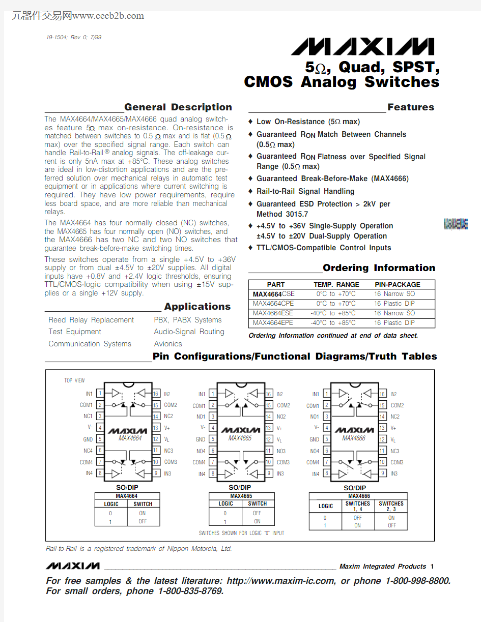
The MAX4664/MAX4665/MAX4666 quad analog switch-es feature 5?max on-resistance. On-resistance is matched between switches to 0.5?max and is flat (0.5?max) over the specified signal range. Each switch can handle Rail-to-Rail ?analog signals. The off-leakage cur-rent is only 5nA max at +85°C. These analog switches are ideal in low-distortion applications and are the pre-ferred solution over mechanical relays in automatic test equipment or in applications where current switching is required. They have low power requirements, require less board space, and are more reliable than mechanical relays.
The MAX4664 has four normally closed (NC) switches,the MAX4665 has four normally open (NO) switches, and the MAX4666 has two NC and two NO switches that guarantee break-before-make switching times.
These switches operate from a single +4.5V to +36V supply or from dual ±4.5V to ±20V supplies. All digital inputs have +0.8V and +2.4V logic thresholds, ensuring TTL/CMOS-logic compatibility when using ±15V sup-plies or a single +12V supply.
Applications
Reed Relay Replacement PBX, PABX Systems Test Equipment
Audio-Signal Routing Communication Systems
Avionics
Features
o Low On-Resistance (5?max)
o Guaranteed R ON Match Between Channels (0.5?max)o Guaranteed R ON Flatness over Specified Signal Range (0.5?max)o Guaranteed Break-Before-Make (MAX4666)o Rail-to-Rail Signal Handling
o Guaranteed ESD Protection > 2kV per Method 3015.7o +4.5V to +36V Single-Supply Operation ±4.5V to ±20V Dual-Supply Operation o TTL/CMOS-Compatible Control Inputs
MAX4664/MAX4665/MAX4666
5?, Quad, SPST,
CMOS Analog Switches
________________________________________________________________Maxim Integrated Products
1
Pin Configurations/Functional Diagrams/Truth Tables
19-1504; Rev 0; 7/99
Ordering Information continued at end of data sheet.
Ordering Information
Rail-to-Rail is a registered trademark of Nippon Motorola, Ltd.
M A X 4664/M A X 4665/M A X 4666
5?, Quad, SPST,
CMOS Analog Switches 2_______________________________________________________________________________________
ABSOLUTE MAXIMUM RATINGS
Note 1:Signals on NC_, NO_, COM_, or IN_ exceeding V+ or V- are clamped by internal diodes. Limit forward-diode current to
maximum current rating.
V+ to GND..............................................................-0.3V to +44V V- to GND..............................................................+0.3V to -44V V+ to V-...................................................................-0.3V to +44V V L to GND........................................(GND - 0.3V) to (V+ + 0.3V)All Other Pins to DGND (Note 1).........(V- - 0.3V) to (V+ + 0.3V) Continuous Current (COM_, NO_, NC_) ........................±100mA Peak Current (COM_, NO_, NC_)
(pulsed at 1ms, 10% duty cycle)...............................±300mA
Continuous Power Dissipation (T A = +70°C)
Narrow SO (derate 8.70mW/°C above +70°C)...............696mW Plastic DIP (derate 10.53mW/°C above +70°C)..............842mW Operating Temperature Ranges
MAX466_C_E ......................................................0°C to +70°C MAX466_E_E....................................................-40°C to +85°C Storage Temperature Range.............................-65°C to +150°C Lead Temperature (soldering, 10sec).............................+300°C
ELECTRICAL CHARACTERISTICS—Dual Supplies
(V+ = +15V, V- = -15V, V L = +5V, V IN_H = +2.4V, V IN_L = +0.8V, T A = T MIN to T MAX , unless otherwise noted. Typical values are at T A = +25°C.) (Note 2)
Stresses beyond those listed under “Absolute Maximum Ratings” may cause permanent damage to the device. These are stress ratings only, and functional operation of the device at these or any other conditions beyond those indicated in the operational sections of the specifications is not implied. Exposure to absolute maximum rating conditions for extended periods may affect device reliability.
ELECTRICAL CHARACTERISTICS—Dual Supplies (continued)
MAX4664/MAX4665/MAX46665?, Quad, SPST,CMOS Analog Switches (V+ = +15V, V- = -15V, V L= +5V, V IN_H= +2.4V, V IN_L= +0.8V, T A= T MIN to T MAX, unless otherwise noted. Typical values are at
T A= +25°C.) (Note 2)
_______________________________________________________________________________________3
M A X 4664/M A X 4665/M A X 4666
5?, Quad, SPST,
CMOS Analog Switches 4_______________________________________________________________________________________
ELECTRICAL CHARACTERISTICS—Single Supply
(V+ = +12V, V- = 0, V L = +5V, V IN_H = +2.4V, V IN_L = +0.8V, T A = T MIN to T MAX , unless otherwise noted. Typical values are at T A = +25°C.)
ELECTRICAL CHARACTERISTICS—Single Supply (continued)
MAX4664/MAX4665/MAX46665?, Quad, SPST,CMOS Analog Switches (V+ = +12V, V- = 0, V L= +5V, V IN_H= +2.4V, V IN_L= +0.8V, T A= T MIN to T MAX, unless otherwise noted. Typical values are at T A= +25°C.)
(Note 2)
Note 2:The algebraic convention, where the most negative value is a minimum and the most positive value a maximum, is used in this data sheet.
Note 3:Guaranteed by design.
Note 4:?R ON= R ON(MAX)- R ON(MIN).
Note 5:Flatness is defined as the difference between the maximum and minimum value of on-resistance as measured over the specified analog signal range.
Note 6:Leakage parameters are 100% tested at maximum-rated hot temperature and guaranteed by correlation at +25°C.
Note 7:Off-isolation = 20log10[V COM_/ (V NC_or V NO_)], V COM_= output, V NC_or V NO_= input to off switch.
Note 8:Between any two switches.
Note 9:Leakage testing at single supply is guaranteed by testing with dual supplies.
_______________________________________________________________________________________5
M A X 4664/M A X 4665/M A X 4666
5?, Quad, SPST,
CMOS Analog Switches 6_______________________________________________________________________________________
Typical Operating Characteristics
(T A = +25°C, unless otherwise noted.)
2.03.02.54.03.55.04.55.56.56.07.0
-20
-10
-5
-15
05
101520
ON-RESISTANCE
V COM (V)
R O N (?)
1.5
2.52.0
3.53.0
4.54.0
5.0
-15
-5
0-10
5
10
15
ON-RESISTANCE vs. V COM
AND TEMPERATURE (DUAL SUPPLIES)
V COM (V)
R O N (?)
421086
12141618
0693121518212427303336
ON-RESISTANCE vs. V COM
(SINGLE SUPPLY)
V COM (V)
R O N (?)
3.0
4.54.03.5
5.05.5
6.06.5
7.07.58.00
4
2
68
10
12
ON-RESISTANCE vs. V COM
AND TEMPERATURE (SINGLE SUPPLY)
V COM (V)
R O N (?)
040201008060120140160180-10-6
-4
-8
-2
2
4
10
ON/OFF TIMES vs. V COM
(DUAL SUPPLIES)
V COM (V)t O N , t O F F (n s )
6
8
0.01
10k 1010.11001k 100k
-40-10520-253550100958065ON/OFF-LEAKAGE CURRENT
vs. TEMPERATURE
TEMPERATURE (°C)
L E A K A G E (p A )
-200
-100200100
0300400500600
-20-10-5-1505101520
CHARGE INJECTION
vs. V V COM (V)
Q (p C )
150
1002502003000
4
6
2
8
10
12
14
ON/OFF TIMES vs. V COM
(SINGLE SUPPLY)
V COM (V)
t O N , t O F F (n s )
5050
807011010090120130140150
101213111415161720
ON/OFF TIMES vs. SUPPLY VOLTAGE
(DUAL SUPPIES)
V+ = -V (V)
t O N , t O F F (n s )
181960
0200100
3004005006000
10
15
5
2025
30
35
40
ON/OFF TIMES vs. SUPPLY VOLTAGE
(SINGLE SUPPLY)
V+ (V)
t O N , t O F F (n s )
8060100120140160-60
-20
-40
20
40
60
80
100ON/OFF TIMES vs. TEMPERATURE
(DUAL SUPPLIES)
TEMPERATURE (°C)t O N , t O F F (n s )
40200.01
10.1
101001k 10k -60
-20
-40
20
40
60
80
100
SUPPLY CURRENT vs. TEMPERATURE
TEMPERATURE (°C)
I +, I - (p A )
-100
0.01
1
10
0.1
100
FREQUENCY RESPONSE
FREQUENCY (MHz)
L O S S (d B )
-90-80-70-60-50-40-30
-20-100200150250300350400
-60
-20
0-40
20406080100
ON/OFF TIMES vs. TEMPERATURE
(SINGLE SUPPLY)
TEMPERATURE (°C)
t O N , t O F F (n s )
10050MAX4664/MAX4665/MAX4666
5?, Quad, SPST,
CMOS Analog Switches
_______________________________________________________________________________________7
Typical Operating Characteristics (continued)
(T A = +25°C, unless otherwise noted.)
M A X 4664/M A X 4665/M A X 4666
5?, Quad, SPST,
CMOS Analog Switches 8_______________________________________________________________________________________
Applications Information
Overvoltage Protection
Proper power-supply sequencing is recommended for all CMOS devices. Do not exceed the absolute maxi-mum ratings, because stresses beyond the listed rat-ings can cause permanent damage to the devices.Always sequence V+ on first, then V-, followed by the logic inputs, NO, or COM. If power-supply sequencing is not possible, add two small signal diodes (D1, D2) in series with supply pins (Figure 1). Adding diodes reduces the analog signal range to one diode drop below V+ and one diode drop above V-, but does not affect the devices’ low switch resistance and low leak-age characteristics. Device operation is unchanged,and the difference between V+ and V- should not exceed 44V. These protection diodes are not recom-mended when using a single supply.
Off-Isolation at High Frequencies
In 50?systems, the high-frequency on-response of these parts extends from DC to above 100MHz, with a typical loss of -2dB. When the switch is turned off, how-ever, it behaves like a capacitor, and off-isolation decreases with increasing frequency. (Above 300MHz,
the switch actually passes more signal turned off than turned on.) This effect is more pronounced with higher source and load impedances.
Figure 1. Overvoltage Protection Using External Blocking Diodes
Pin Description
MAX4664/MAX4665/MAX4666
5?, Quad, SPST,
CMOS Analog Switches
_______________________________________________________________________________________
9
Figure 2. Switching-Time Test Circuit
Above 5MHz, circuit board layout becomes critical,and it becomes difficult to characterize the response of the switch independent of the circuit. The graphs shown in the Typical Operating Characteristics were taken using a 50?source and load connected with BNC connectors to a circuit board deemed “average,”
that is, designed with isolation in mind, but not using stripline or other special RF circuit techniques. For criti-cal applications above 5MHz, use the MAX440,MAX441, and MAX442, which are fully characterized up to 160MHz.
Figure 3. Charge-Injection Test Circuit
M A X 4664/M A X 4665/M A X 4666
5?, Quad, SPST,
CMOS Analog Switches 10______________________________________________________________________________________
Figure 6. Switch Off-Capacitance Test Circuit Figure 7. Switch On-Capacitance Test Circuit
Figure 4. Off-Isolation Test Circuit
Figure 5. Crosstalk Test Circuit
MAX4664/MAX4665/MAX4666
5?, Quad, SPST,
CMOS Analog Switches
Chip Information
TRANSISTOR COUNT: 108
Ordering Information (continued)
Package Information
M A X 4664/M A X 4665/M A X 4666
5?, Quad, SPST,
CMOS Analog Switches Maxim cannot assume responsibility for use of any circuitry other than circuitry entirely embodied in a Maxim product. No circuit patent licenses are implied. Maxim reserves the right to change the circuitry and specifications without notice at any time.
12____________________Maxim Integrated Products, 120 San Gabriel Drive, Sunnyvale, CA 94086 408-737-7600?1999 Maxim Integrated Products
Printed USA
is a registered trademark of Maxim Integrated Products.
Package Information (continued)