G104VN01 V0 工业规格液晶屏

( ) Preliminary Specifications
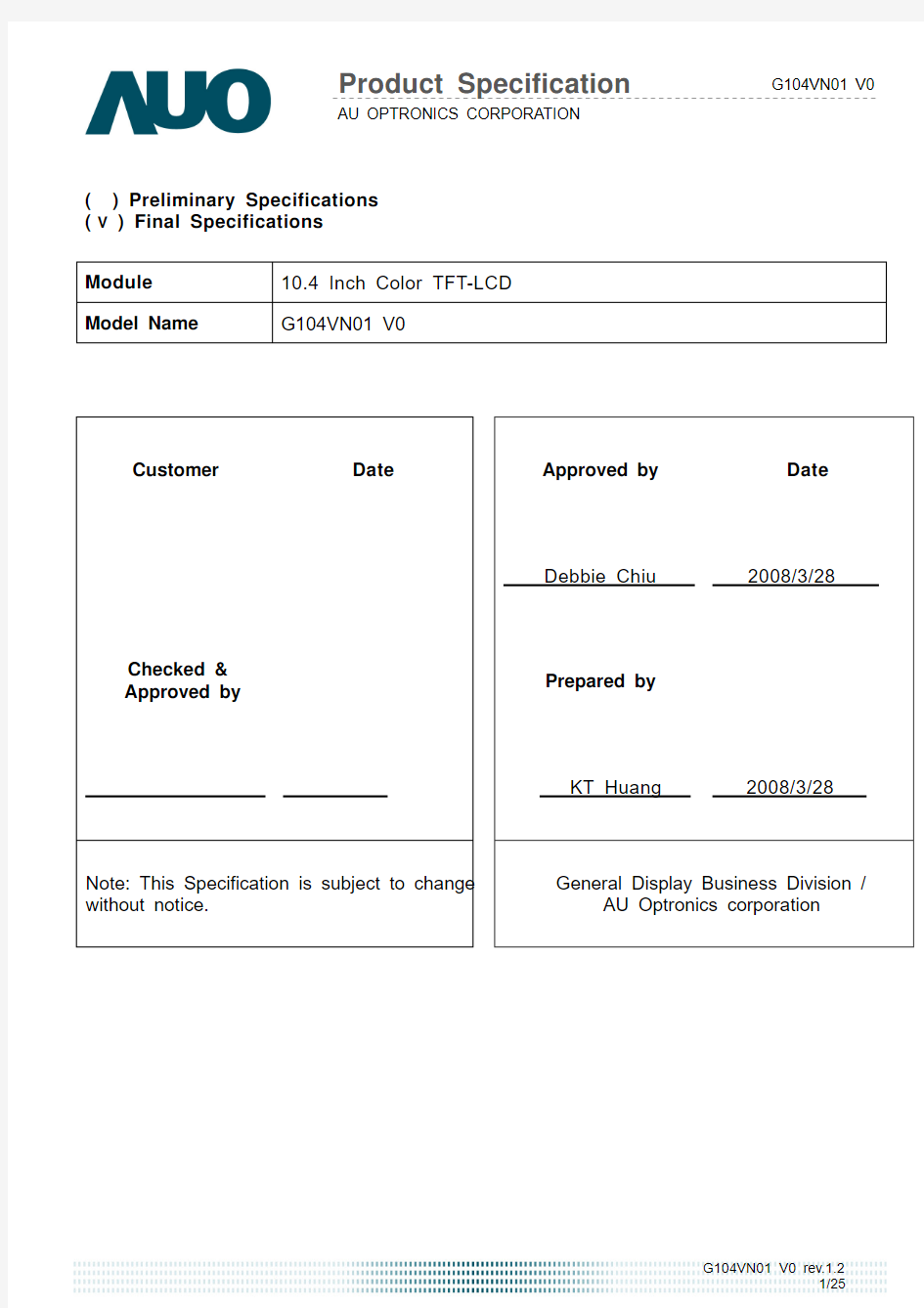
( V ) Final Specifications
Module 10.4 Inch Color TFT-LCD Model Name G104VN01 V0
Customer Date
Checked &
Approved by
Note: This Specification is subject to change without notice. Approved by Date Debbie Chiu 2008/3/28 Prepared by
KT Huang 2008/3/28 General Display Business Division / AU Optronics corporation
Contents
1. Operating Precautions (4)
2. General Description (5)
2.1 Display Characteristics (5)
2.2 Optical Characteristics (6)
3. Functional Block Diagram (9)
4. Absolute Maximum Ratings (10)
4. Absolute Maximum Ratings (10)
4.1 Absolute Ratings of TFT LCD Module (10)
4.2 Absolute Ratings of Environment (10)
5. Electrical Characteristics (11)
5.1 TFT LCD Module (11)
5.2 Backlight Unit (13)
5.2 Backlight Unit (13)
6. Signal Characteristic (15)
6.1 Pixel Format Image (15)
6.2 Scanning Direction (15)
6.3 Signal Description (16)
6.4 The Input Data Format (17)
6.5 Interface Timing (18)
6.6 Power ON/OFF Sequence (19)
7. Connector & Pin Assignment (20)
7.1 TFT LCD Module: Input Connector (20)
7.2 Backlight Unit: Lamp Connector (20)
7.3 Lamp Connector Pin Assignment (20)
8. Reliability Test Criteria (21)
9. Mechanical Characteristics (22)
9.1 LCM Outline Dimension (Front View) (22)
9.2 LCM Outline Dimension (Rear View) (23)
10. Label and Packaging (24)
10.1 Shipping Label (on the rear side of TFT-LCD display) (24)
10.2 Carton Label (24)
11 Safety (25)
11.1 Sharp Edge Requirements (25)
11.2 Materials (25)
11.3 Capacitors (25)
11.4 National Test Lab Requirement (25)
Record of Revision
Version and Date
Page
Old description
New Description
0.1 Apr. 09, 2007 All First draft specification
-
1.0 Sep. 24, 2007 5 Physical Size: 243.0(H)x 176.6(V) x
11.5(D)
Physical Size: 243.0(H)x 176.6(V) x 11.4(D)
Operating and storage temperature range: -30 to +80 Operating and storage temperature range: -30 to +85
6 Contrast Ratio: Typ. 500
Contrast Ratio: Typ. 700
Color / Chromaticity Coordinates: TBD Add Color / Chromaticity Coordinates description
10 Supply Voltage: Max. 5.5
Supply Voltage: Max. 6
Operating Temperature: Max. +80 Operating Temperature: Max. +85 Storage Temperature: Max. +80 Storage Temperature: Max. +85
13
ViCFL (25 o
C): TBD
Add Typ. and Max. CCFL ignition voltage
at 25 o
C
ViCFL (0 o C): N/A
Add Typ. and Max. CCFL ignition voltage
at 0 o C
Note 1, 2, 3, 4 and 5 Modify and restructure the description of Note
18 Clock Frequency: Max. 40 Clock Frequency: Max. 50
Vsync Timing Vertical section Add Pulse width + back porch and Front porch
Hsync Timing Horizontal Section Add Pulse width + back porch and Front porch
Input timing diagram
Modify the input timing diagram 21 High Temperature Operation: 80o
C,300 hours
High Temperature Operation: 85o
C,300 hours
Hot Storage: 80 o
C,300 hours Hot Storage: 85 o
C,300 hours Hot Start Test: 80 o C /1 Hr min. power on/off per 5 minutes, 5 times
Hot Start Test: 85 o C /1 Hr min. power on/off per 5 minutes, 5 times
22 LCM Outline Dimension (Front View) Modify the front view drawing
1.1 Nov. 8, 2007 23 LCM Outline Dimension (Rear View) Add the Pin.1 and Pin.31 position marks
24
Shipping label Add China RoHS mark on shipping label 1.2 Mar. 28, 2008 11
Irush, max. 0.9A
Irush, max 1.2A
1. Operating Precautions
1) Since front polarizer is easily damaged, please be cautious and not to scratch it.
2) Be sure to turn off power supply when inserting or disconnecting from input connector.
3) Wipe off water drop immediately. Long contact with water may cause discoloration or spots.
4) When the panel surface is soiled, wipe it with absorbent cotton or soft cloth.
5) Since the panel is made of glass, it may be broken or cracked if dropped or bumped on hard surface.
6) Since CMOS LSI is used in this module, take care of static electricity and insure human earth when
handling.
7) Do not open nor modify the module assembly.
8) Do not press the reflector sheet at the back of the module to any direction.
9) In case if a module has to be put back into the packing container slot after it was taken out from the
container, do not press the center of the CCFL Reflector edge. Instead, press at the far ends of the
CCFL Reflector edge softly. Otherwise the TFT Module may be damaged.
10) At the insertion or removal of the Signal Interface Connector, be sure not to rotate nor tilt the Interface
Connector of the TFT Module.
11) After installation of the TFT Module into an enclosure (Notebook PC Bezel, for example), do not twist
nor bend the TFT Module even momentary. At designing the enclosure, it should be taken into
consideration that no bending/twisting forces are applied to the TFT Module from outside. Otherwise
the TFT Module may be damaged.
12) Cold cathode fluorescent lamp in LCD contains a small amount of mercury. Please follow local ordinances or
regulations for disposal.
13) Small amount of materials having no flammability grade is used in the LCD module. The LCD module should be
supplied by power complied with requirements of Limited Power Source (IEC60950 or UL1950), or be applied exemption.
14) The LCD module is designed so that the CCFL in it is supplied by Limited Current Circuit (IEC60950 or UL1950).
Do not connect the CCFL in Hazardous Voltage Circuit.
15) Severe temperature condition may result in different luminance, response time and lamp ignition voltage.
16) Continuous operating TFT-LCD display under low temperature environment may accelerate lamp exhaustion
and reduce luminance dramatically.
17) The data on this specification sheet is applicable when LCD module is placed in landscape position.
18) Continuous displaying fixed pattern may induce image sticking. It’s recommended to use screen saver or
shuffle content periodically if fixed pattern is displayed on the screen.
2. General Description
G104VN01 V0 is a Color Active Matrix Liquid Crystal Display composed of a TFT-LCD display, a driver circuit, and a backlight system. The screen format is intended to support VGA (640(H) x 480(V)) screen and 262K colors (RGB
6-bits). All input signals are CMOS interface. Inverter card of backlight is not included.
G104VN01 V0 is designed for industrial display applications.
2.1 Display Characteristics
The following items are characteristics summary on the table under 25 ℃ condition:
Items Unit Specifications
Screen Diagonal [inch] 10.4
Active Area [mm] 211.2(H) x 158.4(V)
Pixels H x V 640x3(RGB) x 480
Pixel Pitch [mm] 0.33 x 0.33
Pixel Arrangement R.G.B. Vertical Stripe
Display Mode TN, Normally White
Nominal Input Voltage VDD [Volt] 3.3V or 5V
Typical Power Consumption [Watt] 6.7W (IRCFL=6.0mA) All black pattern
Weight [Grams] 490g(typ.)
Physical Size [mm] 243.0(H)x 176.6(V) x 11.4(D) (Typ.) Electrical Interface 1ch CMOS
Surface Treatment Anti-glare, Hardness 3H
Support Color 262K colors
Temperature Range
Operating
Storage (Non-Operating) [o C]
[o C]
-30 to +85
-30 to +85
RoHS Compliance RoHS Compliance
2.2 Optical Characteristics
The optical characteristics are measured under stable conditions at 25℃ (Room Temperature):
Item Unit Conditions Min. Typ. Max.
Note White Luminance [cd/m2] IRCFL= 6mA
(center point) 450 -
1 Uniformity % 5 points
75
- 1, 2, 3 Contrast Ratio
700 - 4
[msec]
Rising - 20 30 [msec] Falling - 10 20 Response Time
[msec] Rising + Falling - 30 50 5
[degree] [degree]
Horizontal (Right) CR = 10 (Left)
60 60 70 70 - - Viewing Angle
[degree] [degree]
Vertical (Upper) CR = 10 (Lower) 45 55 55 65 - - 6
Red x 0.55 0.58 0.61 Red y 0.30 0.33 0.36 Green x
0.29 0.32 0.35 Green y 0.53 0.56 0.59 Blue x 0.13 0.16 0.19 Blue y 0.13 0.16 0.19 White x 0.28 0.31 0.34 Color / Chromaticity Coordinates (CIE 1931)
White y
0.30 0.33 0.36
Color Gamut
%
45
-
Note 1: Measurement method
Equipment Pattern Generator, Power Supply, Digital Voltmeter, Luminance meter (SR_3 or equivalent)
Aperture
1with 50cm viewing distance °
Test Point Center Environment < 1 lux
Module Driving
Note 2: Definition of 5 points position (Display active area: 211.2mm (W) x 158.4mm (H))
Note 3: The luminance uniformity of 5 points is defined by dividing the minimum luminance values by the maximum test point luminance
Note 4: Definition of contrast ratio (CR):
Note 5: Definition of response time:
The output signals of photo detector are measured when the input signals are changed from “White” to “Black” (falling time) and from “Black” to “White” (rising time), respectively. The response time interval is between 10% and 90% of amplitudes. Please refer to the figure as below.
Contrast ratio (CR)=
Brightness on the “White” state Brightness on the “Black” state
Minimum Brightness of five points
δW5 = Maximum Brightness of five points
Note 6: Definition of viewing angle
Viewing angle is the measurement of contrast ratio 10, at the screen center, over a 180° horizontal and 180°
≧
vertical range (off-normal viewing angles). The 180° viewing angle range is broken down as below: 90° (θ) horizontal left and right, and 90° (Φ) vertical high (up) and low (down). The measurement direction is typically perpendicular to the display surface with the screen rotated to its center to develop the desired measurement viewing angle.
3. Functional Block Diagram
The following diagram shows the functional block of the 10.4 inch color TFT/LCD module:
4. Absolute Maximum Ratings
4.1 Absolute Ratings of TFT LCD Module
Item Symbol Min Max Unit Logic Voltage Vin -0.3 VDD+0.3 [Volt] Supply Voltage VDD 0 6 [Volt]
4.2 Absolute Ratings of Environment
Item Symbol Min Max Unit Operating Temperature TOP -30 +85 [o C] Operation Humidity HOP 5 90 [%RH] Storage Temperature TST -30 +85 [o C] Storage Humidity HST 5 90 [%RH] Note: Maximum Wet-Bulb should be 39o C and no condensation.
5.1 TFT LCD Module
5.1.1 Power Specification
Symbol
Parameter Min Typ Max Units Remark
3.0 3.3 3.6 VDD Logic/LCD Drive
Voltage 4.5 5.0 5.5 [Volt]
- 220 300 All Black Pattern(VDD=3.3V) IDD VDD Current -
145 200 [mA] All Black Pattern(VDD=5V) I rush LCD Inrush Current
- - 1.2 [A]
Note 1
- 0.73 0.9 All Black Pattern(VDD=3.3V) PDD VDD Power 0.73 0.9 [Watt] All Black Pattern(VDD=5V) VDDrp
Allowable Logic/LCD Drive Ripple Voltage
-
-
100
[mV] p-p All Black Pattern (VDD=3.3V/5V)
Note 1: Irush current measurement condition when LCD supplies 3.3V:
VDD rising time
3.3
Input signals shall be low or Hi-Z state when VDD is off.
Symbol Item Min. Typ. Max. Unit Remark VIH High Input Voltage 0.7VDD - VDD [Volt]
VIL Low Input Voltage 0 - 0.3VDD [Volt]
5.2 Backlight Unit
5.2.1 Parameter guideline for CCFL
Following characteristics are measured under a stable condition using an inverter at 25 (Room Temperature):
℃Symbol Parameter Min.Typ.Max.Unit Remark
IRCFL CCFL operation range 4.5 6.0 7.0 [mA]
rms
(Ta=25o
C) Note 1
FCFL CCFL Frequency 40 50 60 [KHz] (Ta=25o
C) Note 2
ViCFL
(25o C)
(reference)
CCFL Ignition Voltage -740 890
[Volt]
rms
(Ta=25o C)
ViCFL
(0o C)
(reference)
CCFL Ignition Voltage 930 1110
[Volt]
rms
(Ta=0o C) VCFL CCFL Discharge Voltage 440 490 540
[Volt]
rms
(Ta=25o C) Note 3
IRCFL=6mA PCFL
CCFL Power consumption
(inverter excluded)
- 5.88 - [Watt]
(Ta=25o C) Note 3
IRCFL=6mA
Lamp Life 50,000 Hrs
(Ta=25o C) Note 4
IRCFL= 6mA
Note 1: IRCFL is defined as the return current of an inverter. (In Figure. 1)
(Figure. 1: Measurement of return current)
A stable IRCFL is a current without flicker or biasing waveform provided by inverter that ensures the
backlight perform to its specification. The ideal sine waveform should be symmetric in positive and
negative polarities and the asymmetry rate of the inverter waveform should be below 10%.
Reference
DC Bias = (| Ip – I-p| / Irms ) x 100 % <10%
Crest Factor = Ip or (I-p) / Irms should have the range within 1.414 + 10%
It is recommended to use the inverter with detection circuit ( ie: balance and protection circuit) to avoid
overvoltage, overcurrent, or mismatching waveform.
Note 2: CCFL frequency should be carefully determined to avoid interference between inverter and TFT LCD.
Higher frequency will induce higher leakage current and further impact lamp life.
Note 3: Calculator value for reference (IRCFLx2 VCFL=PCFL).
Note 4: The definition of lamp life means when any of following conditions happen:
a) Luminance falls to 50% or less of the initial value.
b) Normal lighting is no more available (flickering, pink lighting, no lighting, etc.)
c) Lamp voltage or lighting start voltage exceeds the specified value.
Lamp life time shortens according to
a) Placing methodology: mercury is unevenly distributed in portrait mounting
b) Environmental condition: low temperature reduces the presence of mercury vapor, which results in
approximately lamp life of 1,000 hours
c) CCFL surface temperature: Presence of gradient in lamp surface temperature causes uneven mercury
migration
d) Inverter design: its resonance capacitor should be fine-tuned with the impedance of CCFL
e) Over driving current (> 7 mA) shortens lamp life time dramatically.
Note 5: The display is with dual lamp design, and the CCFL current in above table refers to each lamp
6. Signal Characteristic 6.1 Pixel Format Image
Following figure shows the relationship between input signal and LCD pixel format.
1st
Pixel
2nd
Pixel
639th
Pixel
640
th
Pixel
1
st
Line R G B R G B
R G B R G B
480th
Line
R G B R G B
R G B R G B
6.2 Scanning Direction
The following figures show the image seen from the front view. The arrow indicates the direction of scan.
Fig. 1 Normal scan (DPSH = High, DPSV=Low) Fig. 2 Reverse scan (DPSH = Low, DPSV=Low)
Fig. 3 Reverse scan (DPSH = High, DPSV=High)
Fig. 4 Reverse scan (DPSH = Low, DPSV=High)
6.3 Signal Description
Pin no Symbol Function Etc.
1 GND Ground
2 CK Clock signal for sampling each data signal
3 Hsync Horizontal synchronous signal
4 Vsync Vertical synchronous signal
5 GND Ground
6 R0 RED data signal (LSB)
7 R1 RED data signal
8 R2 RED data signal
9 R3 RED data signal
10 R4 RED data signal
11 R5 RED data signal (MSB)
12 GND Ground
13 G0 GREEN data signal (LSB)
14 G1 GREEN data signal
15 G2 GREEN data signal
16 G3 GREEN data signal
17 G4 GREEN data signal
18 G5 GREEN data signal (MSB)
19 GND Ground
20 B0 BLUE data signal (LSB)
21 B1 BLUE data signal
22 B2 BLUE data signal
23 B3 BLUE data signal
24 B4 BLUE data signal
25 B5 BLUE data signal(MSB)
26 GND Ground
27 ENAB Signal to settle the horizontal display position
28 VDD +3.3V / +5.0V power supply
29 VDD +3.3V / +5.0V power supply
30 DPSH Horizontal reverse scan control signal
31 DPSV Vertical reverse scan control signal
6.4 The Input Data Format
G104VN01 V0 rev.1.2
18/25
6.5 Interface Timing
6.5.1 Timing Characteristics
Signal
Parameter Symbol Min. Typ. Max. Unit
Remark Clock Timing
Clock Frequency
1/ T Clock
20 25.2 28.33 MHz
Period
T VS 520 525
560 Active
T VSD
480 480
480 Pulse width + back porch T VSW +T VSB
35
35 35
Vsync Timing
Vertical
Section
Front porch T VSF 5
10 45 T Line
Period
T HS
770 800
900 Active
T HSD
640 640 640 Pulse width + back porch T HSW +T HSB
100 100 100 Hsync Timing
Horizontal Section
Front porch
T HSF
30
60
160
T Clock
6.5.2 Input Timing Diagram
6.6 Power ON/OFF Sequence
VDD power and lamp on/off sequence is as below. Interface signals are also shown in the chart. Signals from any
system shall be Hi-Z state or low level when VDD is off.
Power ON/OFF sequence timing
Value
Parameter
Min. Typ. Max. Units T1 0.5 - 10 ms T2 0 - 50 ms T3 180 - - ms T4 180 - - ms T5 0 - 50 ms T6 0 - 10 ms T7
500
-
-
ms
The above on/off sequence should be applied to avoid abnormal function in the display. Please make sure to turn off the power when you plug the cable into the input connector or pull the cable out of the connector.
Power Supply VDD Signal
Backlight On
7. Connector & Pin Assignment
Physical interface is described as for the connector on module. These connectors are capable of accommodating the following signals and will be following components.
7.1 TFT LCD Module: Input Connector
CN1 connector
Connector Name / Designation Signal Connector
Manufacturer Hirose or compatible
Connector Model Number DF9B-31P-1V or compatible
Adaptable Plug DF9B-31S-1V or compatible
7.2 Backlight Unit: Lamp Connector
CN2 connector
Connector Name / Designation Lamp Connector
Manufacturer JST or compatible
Connector Model Number BHR-03VS-1 or compatible
Mating Model Number B-BHS-1-TB or compatible
7.3 Lamp Connector Pin Assignment
CN2 connector (backlight): BHS-03VS-1
Pin # Symbol Cable color Signal Name
1 H Pink CCFL power supply(H.V.)
2 NC No connection
3 L White CCFL power supply(GND)
Pin # Symbol Cable color Signal Name
1 H Blue CCFL power supply(H.V.)
2 NC No connection
3 L Black CCFL power supply(GND)
显示器接口知识全解
显示器接口知识全解 显示器接口是指显示器和主机之间的接口,通常有DVI、HDMI和15针D-SubVGA三种: DVI数字输入接口:DVIDigital Visual Interface,数字视频接口是近年来随着数字化显示设备的发展而发展起来的一种显示接口。普通的模拟RGB接口在显示过程中,首先 要在计算机的显卡中经过数字/模拟转换,将数字信号转换为模拟信号传输到显示设备中,而在数字化显示设备中,又要经模拟/数字转换将模拟信号转换成数字信号,然后显示。 在经过2次转换后,不可避免地造成了一些信息的丢失,对图像质量也有一定影响。而 DVI接口中,计算机直接以数字信号的方式将显示信息传送到显示设备中,避免了2次转 换过程,因此从理论上讲,采用DVI接口的显示设备的图像质量要更好。另外DVI接口实 现了真正的即插即用和热插拔,免除了在连接过程中需关闭计算机和显示设备的麻烦。现 在很多液晶显示器都采用该接口,CRT显示器使用DVI接口的比例比较少。需要说明的是,现在有些液晶显示器的DVI接口可以支持HDCP协议,为看有版权的高清电影电视打下基础。 HDMI数字输入接口:HDMI的英文全称是“High Definition Multimedia”,中文的 意思是高清晰度多媒体接口。HDMI接口可以提供高达5Gbps的数据传输带宽,可以传送无压缩的音频信号及高分辨率视频信号。同时无需在信号传送前进行数/模或者模/数转换, 可以保证最高质量的影音信号传送。应用HDMI的好处是:只需要一条HDMI线,便可以同 时传送影音信号,而不像现在需要多条线材来连接;同时,由于无线进行数/模或者模/数 转换,能取得更高的音频和视频传输质量。对消费者而言,HDMI技术不仅能提供清晰的画质,而且由于音频/视频采用同一电缆,大大简化了家庭影院系统的安装。HDMI接口支持HDCP协议,为看有版权的高清电影电视打下基础。 2002年的4月,日立、松下、飞利浦、Silicon Image、索尼、汤姆逊、东芝共7家 公司成立了HDMI组织开始制定新的专用于数字视频/音频传输标准。2002年岁末,高清晰数字多媒体接口High-definition Digital Multimedia InterfaceHDMI 1.0标准颁布, 到2021底已经颁布了1.3版本,主要变化在于近一步加大带宽,以便传输更高分辨率和 色深。HDMI在针脚上和DVI兼容,只是采用了不同的封装。与DVI相比,HDMI可以传输 数字音频信号,并增加了对HDCP的支持,同时提供了更好的DDC可选功能。HDMI支持 5Gbps的数据传输率,最远可传输15米,足以应付一个1080p的视频和一个8声道的音频信号。而因为一个1080p的视频和一个8声道的音频信号需求少于4GB/s,因此HDMI还有很大余量。这允许它可以用一个电缆分别连接DVD播放器,接收器和PRR。此外HDMI支持EDID、DDC2B,因此具有HDMI的设备具有“即插即用”的特点,信号源和显示设备之间会 自动进行“协商”,自动选择最合适的视频/音频格式。 15针D-SubVGA输入接口:也叫VGA接口,CRT彩显因为设计制造上的原因,只能接 受模拟信号输入,最基本的包含R\G\B\H\V分别为红、绿、蓝、行、场5个分量,不管以 何种类型的接口接入,其信号中至少包含以上这5个分量。大多数PC机显卡最普遍的接 口为D-15,即D形三排15针插口,其中有一些是无用的,连接使用的信号线上也是空缺
常用液晶屏接口定义
各种液晶屏接口定义 资料从屏的接口样式简单区分屏接口类型的方法 接口, 类型, 样式 从屏的接口样式简单区分屏接口类型的方法 (1)TTL屏接口样式: D6T(单6位TTL):31扣针,41扣针。对应屏的尺寸主要为笔记本液晶屏(8寸,10寸,11寸,12寸),还有部分台式机屏15寸为41扣针接口。 S6T(双6位TTL):30+45针软排线,60扣针,70扣针,80扣针。主要为台式机的14寸,15寸液晶屏。 D8T(单8位TTL):很少见 S8T(双8位TTL):有,很少见80扣针(14寸,15寸) (2)LVDS屏接口样式: D6L(单6位LVDS):14插针,20插针,14片插,30片插(屏显基板100欧姆电阻的数量为4个)主要为笔记本液晶屏(12寸,1 3寸,14寸,15寸) D8L(单8位LVDS):20插针(5个100欧姆)(15寸) S6L(双6位LVDS):20插针,30插针,30片插(8个100欧姆)(14寸,15寸,17寸) S8L(双8位LVDS):30插针,30片插(10个100欧姆电阻)(17寸,18寸,19寸,20寸,21寸) (3)RSDS屏接口样式: 50排线,双40排线,30+50排线。主要为台式机(15寸,17寸)液晶屏。 常用液晶屏接口定义 20PIN单6定义: 1:电源2:电源3:地4:地5:R0- 6:R0+ 7:地8:R1- 9:R1+ 10:地11:R2- 12:R2+ 13:地14:CLK- 15:CLK+ 16空17空18空19 空20空 每组信号线之间电阻为(数字表100欧左右)指针表20 -100欧左右(4组相同阻值) 20PIN双6定义: 1:电源2:电源3:地4:地5:R0- 6:R0+ 7:R1- 8:R1+ 9:R2- 10:R2+ 11:CLK- 12:CLK+ 13:RO1- 14:R O1+ 15:RO2- 16:RO2+ 17:RO3- 18:RO3+ 19:CLK1- 20:CLK1+ 每组信号线之间电阻为(数字表100欧左右)指针表20 -100欧左右(8组相同阻值) 20PIN单8定义: 1:电源2:电源3:地4:地5:R0- 6:R0+ 7:地8:R1- 9:R1+ 10:地11:R2- 12:R2+ 13:地14:CLK- 15:CLK+ 16:R3- 17:R3+ 每组信号线之间电阻为(数字表100欧左右)指针表20 -100欧左右(5组相同阻值) 30PIN单6定义: 1:空2:电源3:电源4:空5:空6:空7:空8:R0- 9:R0+ 10:地11:R1- 12:R1+ 13:地14:R2- 15:R2+ 16:地17:CLK- 18:CLK+ 19:地20:空- 21:空22:空23:空24:空25:空26:空27:空28空29空30空每组信号线之间电阻为(数字表100欧左右)指针表20 -100欧左右(4组相同阻值) 30PIN单8定义: 1:空2:电源3:电源4:空5:空6:空7:空8:R0- 9:R0+ 10:地11:R1- 12:R1+ 13:地14:R2- 15:R2+ 16:地17:CLK- 18:CLK+ 19:地20:R3- 21:R3+ 22:地23:空24:空25:空26:空27:空28空29空30空
友达5.7寸液晶屏G057VTN01 V0规格书-杭州旭虹科技有限公司
G057VTN01 V0 Color TFT-LCD Module 5.7” VGA Landscape LED Backlight Wide Temperature Range Mercury-free solution RoHS and Halogen-free Compliance High Shock/Vibration Resistance Outline and Interface are fully compatible with G057VN01 serials (Preliminary) Size (inch) 5.7” Model G057VN01 V210 Resolution (pixel) 640(RGB) x 480 Active Area (mm) 115.2(H) x 86.4(V) Pixel Pitch (mm) 0.18 x 0.18 Mode TN LCD Surface Anti-Glare, Hardness 3H Number of Colors 262K View Angle (L/R/U/D) 80/80/70/70 (typ.) Brightness(nit) (25℃) 500(min.), 600 (typ.) Contrast Ratio (25℃) 800:1 (typ.) Response Time (ms) 25 (typ.) LED Life (hrs.) 50K Power Consumption (W) 3.74W Supply Voltage (V) 3.3V Storage Temp. (℃) -30 ~ 85 Operation Temp. (℃) -30 ~ 85 Outline Dimension (mm) 144.0(H) x 104.6(V) x 12.3(D) (typ.) Weight (g) 150g (typ.), 165g (max.) Interface CMOS
lvds液晶屏幕接口详细讲解
1.LVDS输出接口概述 液晶显示器驱动板输出的数字信号中,除了包括RGB数据信号外,还包括行同步、场同步、像素时钟等信号,其中像素时钟信号的最高频率可超过28MHz。采用TTL接口,数据传输速率不高,传输距离较短,且抗电磁干扰(EMI)能力也比较差,会对RGB数据造成一定的影响;另外,TTL多路数据信号采用排线的方式来传送,整个排线数量达几十路,不但连接不便,而且不适合超薄化的趋势。采用LVDS输出接口传输数据,可以使这些问题迎刃而解,实现数据的高速率、低噪声、远距离、高准确度的传输。 那么,什么是LVDS输出接口呢?LVDS,即Low Voltage Differential Signaling,是一种低压差分信号技术接口。它是美国NS公司(美国国家半导体公司)为克服以TTL电平方式传输宽带高码率数据时功耗大、EMI电磁干扰大等缺点而研制的一种数字视频信号传输方式。 LVDS输出接口利用非常低的电压摆幅(约350mV)在两条PCB走线或一对平衡电缆上通过差分进行数据的传输,即低压差分信号传输。采用LVDS输出接口,可以使得信号在差分PCB线或平衡电缆上以几百Mbit/s的速率传输,由于采用低压和低电流驱动方式,因此,实现了低噪声和低功耗。目前,LVDS输出接口在17in及以上液晶显示器中得到了广泛的应用。 2.LVDS接口电路的组成 在液晶显示器中,LVDS接口电路包括两部分,即驱动板侧的LVDS输出接口电路(LVDS发送器)和液晶面板侧的LVDS输入接口电路(LVDS接收器)。LVDS发送器将驱动板主控芯片输出的17L电平并行RGB数据信号和控制信号转换成低电压串行LVDS信号,然后通过驱动板与液晶面板之间的柔性电缆(排线)将信号传送到液晶面板侧的LVDS接收器,LVDS接收器再将串行信号转换为TTL电平的并行信号,送往液晶屏时序控制与行列驱动电路。图1所示为LVDS接口电路的组成示意图。
OLED2.4寸显示屏 液晶屏 规格书
、结构尺寸Structure Size 一5V 供电5V IO 电平二、接口定义Pin Assignment(P2&P3)序号(No.) 定义(SYMBOL )说明(Description )1 VCC3.3数字电路电源电压Power Supply for Logic Circuit 2 VCC3.3数字电路电源电压Power Supply for Logic Circuit 3 EN 模块13v OLED 供电使能信号,高有效OLE Panel Power Enable Signal active High to Enable ,默认内部弱上拉,可不接。4 GND 数字电路电源地Ground of Logic Circuit 5 CS 片选信号Chip Select 低有效,6 RES 复位信号Power Reset 低有效,需IO 引脚控制7 D/C 数据与命令控制信号Data/Command Control 高为数据,低为命令。需IO 引脚控制8 GND 数字电路电源地Ground of Logic Circuit 9 SCLK SPI 时钟信号Serial Clock of SPI 。需IO 引脚控制10SDIN SPI 输入信号Serial Data of SPI 。需IO 引脚控制 OLED2.4寸1309_3.3V
一、产品介绍General Specifications Diagonal Size尺寸 2.4” Color颜色Yellow、Green、Blue、White Type类型Monochrome Pixel Number分辨率128x64 Module Size(mm)模组尺寸62.1×53.3×9 Active Size(mm)显示区域55.01×27.49 Driver IC驱动IC SSD1309 Interface接口4_Wire SPI Supply Voltage供电电压 3.3V Voltage Range建议电压范围 1.65V~3.3V Max Voltage最大极限电压4V Min Voltage最小极限电压 1.65V View Angle视角>160degree全视角 Contrast对比度>10000:1 Brightness(cd/m2)亮度(绿色)120(Typ)@13V(20000Hours) Power功耗由点亮的像素决定 30%像素点亮<260mw 50%像素点亮<345mw 100%像素点亮(实际使用中用不到)<515mw Brightness(cd/m2)(黄色)80(Typ)@13V(15000Hours) Power功耗由点亮的像素决定 30%像素点亮<260mw 50%像素点亮<380mw 100%像素点亮(实际使用中用不到)<590mw Brightness(cd/m2)(白色)80(Typ)@13V(30000Hours) Power功耗由点亮的像素决定 30%像素点亮<300mw 50%像素点亮<440mw 100%像素点亮(实际使用中用不到)<690mw Brightness(cd/m2)(蓝色)80(Typ)@13V(15000Hours) Power功耗由点亮的像素决定 30%像素点亮<325mw 50%像素点亮<470mw 100%像素点亮(实际使用中用不到)<720mw Weight(g)重量8.6 Assembly连接方式10Pin1.0mm FPC Connector and2.54mm Metal pins
经典-液晶屏型号列表
经典-液晶屏型号列表.txt我们用一只眼睛看见现实的灰墙,却用另一只眼睛勇敢飞翔,接近梦想。男人喜欢听话的女人,但男人若是喜欢一个女人,就会不知不觉听她的话。 制造商型号尺寸针数分辨率 LG LM171W02 17.1 30P(片插) 未测(16:9) LG LM171W02 17.1 30P(片插) 未测(16:9) AU LP171W01 17 LG LP171WX2 17 Hitachi(日立) LQ154M1LW02 15.4 30P 1920*1200 Hitachi(日立) LTN154E1-L01 15.4 20P 1280*1024 Hitachi(日立) LTN154P1-L01 15.4 30P(片插) 1680*1050 Samsung(三星) LTN154U1-L01 15.4 30P(片插) 1680*1200 Samsung(三星) TX39D97V 15.4 30P(片插) 1400*1050 Sharp(夏普) TX39D98VC1FAA 15.4 30P 1680*1050 AU B152EW01 15.2 20P 1280*854 Samsung(三星) LTN152W1-L01 15.2 20P 1280*854 IBM 47L8130(ITSX93D) 15.1 30P 1400*1050 IBM 47L8130(ITSX93D) 15.1 30P 1400*1050 IBM 47L8140(ITSX93C) 15.1 IBM 47L8150(ITSX93D) 15.1 30P 1400*1050 IBM 47L8160(ITSX93D) 15.1 30P 1400*1050 IBM 47L8160(ITSX93D) 15.1 30P 1400*1050 LG AA151XB01 15.1 100P(扣针) 1024*768 LG LM150X06-A4C4 15.1 41 1024*768 NEC NL10276AC30-03L 15.1 25P 1024*768 NEC 07K2150(IAUX14S) 15 30P(片插) 1600*1200 NEC 07K2510(ITS95L) 15 Acer(宏基) 07K6767(ITSX95C) 15 30P 1400*1050 Acer(宏基) 07K6767(ITSX95C) 15 30P 1400*1050 AU 07N2150(IASX12S) 15 30P(片插) 1280*1024 AU AA150XC01 15 20P(两排) 1024*768 AU B150PG01 15 30P(片插) 1400*1050 Fujitsu(富士通) B150PN01 15 30P(片插) 1400*1050 Fujitsu(富士通) B150PN01 15 30P(片插) 1400*1050 Fujitsu(富士通) B150XG01 15 30P(片插) 1024*768 Fujitsu(富士通) B150XN01 15 20P 1024*768 HannStar CLAA150PA01 15 20P 1400*1050 HannStar HLD1505-010120 15 20P 1024*768 HannStar HLD1505-020120 15 20P 1024*768 HannStar HSD150MX14 15 20P HannStar HSD150MX41 15 60扣双灯 HannStar HSD150MX46 15 双排软插 4灯 Hitachi(日立) HSD150PK12 15 30P(片插) 1400*1050 Hitachi(日立) HT15X31-100 15 20P 1024*768 Hitachi(日立) HT15X31-100 15 20P 1024*768
液晶屏维修
关于LCD液晶显示屏的接口原理 1 所有TFT-LCD的数据接口种类: 单TTL6位(8位)双TTL6位(8位)单LVDS6位(8位)双 LVDS6位(8位)单TMDS6位(8位)双TMDS6位(8位) 还有最新出来的标准RSDS 6位和8位是用来表示屏能显示颜色多少,6位屏可以显示颜色为2的6次方X2的6次方X2的6次方分别代表R G B 三基色,算下来 6位屏最多可以显示的颜色为262144种颜色,8位屏为16777216 种颜色。屏显示颜色的多少只和屏的位数有关。 我们本本用的屏一般都是6位的。 早期的本本都是用12寸以下的屏,该种屏分辩率一般为640X480(VGA) 800X600(SVGA),采用的接口为单TTL6位,屏上接针脚为41针和31针,12寸以41针居多(800X600),10寸以31针居多(640X480)。 TTL信号是TFT-LCD能识别的标准信号,就算是以后用到的LVDS TMDS都是在它的基础上编码得来的。TTL信号线一共有22根(最 少的,没有算地和电源的)分另为R G B 三基色信号,两个HS VS 行场同步信号,一个数据使能信号DE 一个时钟信号CLK, 其中R G G三基色中的每一基色又根据屏的位数不同,而有不同的数据线数(6位,和8位之分)6位屏和8位屏三基色分别有R0-- R5(R7) G0--G5(G7) B0--B5(B7)三基色信号是颜色信号,接错会使屏显示的颜色错乱。另外的4根信号(HS VS DE CLK)是控制信号,接错会使屏点不亮,不能正常显示。 由于TTL信号电平有3V左右,对于高速率的长距离传输影响很大,且抗干扰能力也比较差。所以之后又出现了LVDS接口的屏, L VDS也分单通只要是XGA以上分辩率的屏都是用LVDS方式。 道,双通道,6位,8位,之分,原理和TTL分法是
P6户外全彩LED显示屏规格书
P6户外表贴全彩LED显示屏规格书 绿色大地P6户外表贴全彩LED显示屏显著特点: ■采用高端优质芯片,屏体亮度达6500CD每平方以上绿色大地照明科技充分满足户外亮度要求;亮度100级可调。 ■采用高端电源供应商电源,100-230V宽电压输入,切实保证屏体供电稳定。 ■与IC行业巨头台湾聚积携手,装配高精度驱动芯片,显示画面展现完美的色彩一致性。■采用行业领先控制系统,真正实现逐点校正功能。 ■箱体融入最先进设计理念,结构轻巧,安装便捷,样式美观。 ■全新面罩设计,大大提升屏体对比度及平整度,同时新款面罩具有强劲的抗干扰与抗老化功能。 ■PCB板精选板材,1.5 OZ铜厚,加上独特的PCB板设计工艺,使显示屏稳定性更高、节能性更强、功耗更低。
P6户外表贴屏箱体(480*480MM)4*2个箱体效果图
P6户外表贴显示屏还有如下特点 1)、系统设计先进合理,显示效果清晰稳定,安装维护方便。 2)、全天候工作:色彩逼真、刷新频率高、防静电、散热效果好、性价比高。 3)、显示方式:左右移动、上下移动、左拉幕、右拉幕、中开合、闪烁、即显等多种方式。 4)、使用节目编辑播放软件,可通过、鼠标编辑、增加、删除和修改文字、图形、图像等信息。编排的内容存于控制卡, 信息播放按节目表自动循环显示。 5)、发光亮度强:发光强度强,并且亮度可调。 6)、视角度好:在水平和垂直均有较大的可视角度,这对水平分布广和高度落差较大的环境均适合。 7)、效果好:采用非线性逐点校正技术,文字更清晰、层次感更强; 8)、可靠性强:采用分布式扫描技术和模块化设计技术,可靠性、稳定性更高; 9)、显示模式多样化:支持多种显示模式; 10)、操作方便:电脑编辑内容发送到系统控制卡,就可显示编辑的内容,系统操作十分方便。 11)、适用范围:商场、企业、学校、舞台、银行、证券、公安、交通、工商、电力、海关、 医院、公园、机场、车站、 体育场馆等领域户外租赁显示。 P3全彩显示屏技术参数 LED 屏体波长控制在2.5nm 之内,屏体亮度≥ 6500cd/㎡
12864LCD液晶显示屏中文资料
12864LCD液晶显示屏中文资料 一、概述 二、带中文字库的128X64是一种具有4位/8位并行、2线或3线串行多种接口方式,内部含有国标一级、二级简体中文字库的点阵图形液晶显示模块;其显示分辨率为128×64, 内置8192个16*16点汉字,和128个16*8点ASCII字符集.利用该模块灵活的接口方式和简单、方便的操作指令,可构成全中文人机交互图形界面。可以显示8×4行16×16点阵的汉字. 也可完成图形显示.低电压低功耗是其又一显著特点。由该模块构成的液晶显示方案与同类型的图形点阵液晶显示模块相比,不论硬件电路结构或显示程序都要简洁得多,且该模块的价格也略低于相同点阵的图形液晶模块。 三、基本特性: (1)、低电源电压(VDD:+3.0--+5.5V)(2)、显示分辨率:128×64点(3)、内置汉字字库,提供8192个16×16点阵汉字(简繁体可选) (4)、内置 128个16×8点阵字符(5)、2MHZ时钟频率(6)、显示方式:STN、半透、正显(7)、驱动方式:1/32DUTY,1/5BIAS (8)、视角方向:6点(9)、背光方式:侧部高亮白色LED,功耗仅为普通LED的1/5—1/10 (10)、通讯方式:串行、并口可选(11)、内置DC-DC转换电路,无需外加负压(12)、无需片选信号,简化软件设计(13)、工作温度: 0℃ - +55℃ ,存储温度: -20℃ - +60℃ 模块接口说明: *注释1:如在实际应用中仅使用串口通讯模式,可将PSB接固定低电平,也可以将模块上的J8和“GND”用焊锡短接。 *注释2:模块内部接有上电复位电路,因此在不需要经常复位的场合可将该端悬空。 *注释3:如背光和模块共用一个电源,可以将模块上的JA、JK用焊锡短接。 2.2并行接口
液晶屏ZJ070NA-01P规格书
CHIMEI INNO L U X DISPLAY CORPORATION LCD MODULE SPECIFICATION Customer: Model Name: ZJ070NA-01P Date: 2012/01/11 Version: 01 ■Preliminary Specification □Final Specification For Customer ’s Acceptance Approved by Comment Approved by Reviewed by Prepared by Charlie Chou 2012/02/01 Wenyi Wang 2012/02/01 David Lee 2012/01/31 深显实业有限公司 https://www.360docs.net/doc/308955712.html,
CHIMEI InnoLux copyright 2004 All rights reserved, Copying forbidden. Record of Revision Version Revise Date Page Content Pre-Spec.01 2012/01/11 Initial Release.
CHIMEI INNO L U X Contents 1. General Specifications (1) 2. Pin Assignment (2) 3. Operation Specifications (5) 3.1. Absolute Maximum Ratings (5) 3.1.1. Typical Operation Conditions (6) 3.1.2. Current Consumption (7) 3.1.3. Backlight Driving Conditions (7) 3.2. Power Sequence (8) 3.3. Timing Characteristics (9) 3.3.1. AC Electrical Characteristics (9) 3.3.2. Input Clock and Data Timing Diagram (9) 3.3.3. DC Electrical Characteristics (10) 3.3.4. Timing (11) 3.3.5. Data Input Format (12) 4. Optical Specifications (13) 5. Reliability Test Items (17) 6. General Precautions (18) 6.1. Safety (18) 6.2. Handling (18) 6.3. Static Electricity (18) 6.4. Storage (18) 6.5. Cleaning (18) 7. Mechanical Drawing (19) 8. Package Drawing (20) 8.1. Packaging Material Table (20) 8.2. Packaging Quantity (20) 8.3. Packaging Drawing (21)
液晶屏型号参考列表大全
1.5CLAA015CB01AG CPT 128x128200cd/m2 200:1 18bit 1.5LH152J02LG 128x12835/15 45/45 27.26x27.26 1.5LKC33TMK6YT NAN 128x128LED Backlight T Tomato TL1771 1.5LM15TGFNZ26SHA 128x128120cd/m240:126.1x28.151.5A015AN04AUO 280x220170cd/m2300:115/35 45/4529.96x2 2.66LED Backlight T 1.5A015AN01AUO 280x220200cd/m2150:110/30 45/4529.50x22.2010,000T 1.5A015BL102AUO 502x240170cd/m2300:150/50 20/701.7A017CN01AUO 480x240250cd/m2300:145/45 15/35 34.08x25.56 LED Backlight 1.8CLAA018DE01AG CPT 128x160200cd/m2 300:1 18bit 1.8LKC34ZMH8YS NAN 128x160LED Backlight T MagnaChip IS2341 1.8LMS179FF0SAM 128x160240cd/m2200:131.5x4 2.35 1.8CLAA018FE01AG CPT 176x220200cd/m2200:118bit 1.8A018AN03AUO 280x220240cd/m2150:110/30 45/4535.60x26.60 T 1.8A018AN03V1AUO 280x220240cd/m2150:140/40 10/301.8A01AN02V2AUO 280x22050cd/m2 90:1 45/45 10/301.9LH190Q01LG 240x32085/85 85/85 28.8x38.42.0CLAA020FB01AG CPT 176x220200cd/m2300:12.0LH200J02LG 176x220200cd/m2 350:1 35/15 45/45 31.68x39.60 2.0LKC53TML7YT NAN 176x220LED Backlight T Sam S6D0118IC 2.0PNG20CW PALM 176x220200cd/m2 31.68x39.60LED Backlight HX8309A 2.0LMS200EF0SAM 176x22031.68x39.602.0LQ020QCXX20 SHA 176x22050cd/m2400:131.68x39.602.0TFT6987UCFDFW-P-G-F-LED TRU 176x220114cd/m2350:135/15 45/4533.90x42.10LED Backlight TR 2.0TFT8285UCTDFW-P-G-F-LED TRU 176x220220cd/m2300:145/15 45/45 33.90x42.10 LED Backlight T 2.0CLAA020GA01AW CPT 240x320200cd/m2200:1RGB I/F 2.0LH200Q04LG 240x320250cd/m2350:185/85 85/8530.6x40.82.0LH200Q06-A LG 240x320250cd/m2400:135/15 45/4530.6x40.82.0A020CN01AUO 480x240250cd/m2300:135/15 45/4539.84x29.88LED Backlight 2.0A020BL01AUO 640x240200cd/m2300:150/50 20/7040.64x30.48LED Backlight 2.2LH220J01LG 176x220200cd/m2 350:115/35 45/4534.848x43.56 2.2OGM-N500ODT 176x220250:115/35 45/45 LED Backlight 2.2LMS220EF0SAM 176x220240cd/m2350:134.85x43.562.2LQ022B8UD05 SHA 176x220125cd/m260:130/30 60/6034.848x43.56LED Backlight 2.2TFT8001UCFDFW-P-G-F-LED TRU 176x220300:135/15 45/4539.10x47.86 LED Backlight TR 2.2CLAA022GA01AG CPT 240x320200cd/m2300:118bit 2.2LH220Q12LG 240x320400cd/m2350:115/35 45/453 3.84x45.122.2LH220Q13LG 240x320400cd/m2400:1 85/85 85/85 33.84x45.12 2.2LKC35TMK1MT NAN 240x320LED Backlight T Himax HX8312A Brigthness Contrast Size Supplier Format / Remark Model Display Area Viewing Angle (U/D L/R) Lamp Life Time Display Mode TR=Transflective T=Transmissive Resolution
常见LVDS屏接口定义
2 常见屏的接口 LVDS接口: 比较常见的接口,有14针插接口,20P针插、30针插和片插等多为LVDS接口LVDS常用的驱动板: 2023(支持17寸以下含17寸的所有LVDS屏VGA烧录模式) 2025(支持19寸以下含19寸以下的所有LVDS屏VGA烧录模式) NTA91B(支持22寸或1680*1050以下的所有LVDS屏VGA烧录模式) 2621免程序驱动板(直接跳线就可支持14-19等LVDS屏免烧录) TTL接口:(与LVDS的屏线区别TTL的屏线相对较多) TTL屏要求驱动板输入单或双6位/8位的三基色的TTL电平,所以连接线用得比较多,一般有31扣41扣30软排线+40软排线60扣70扣80扣等,特点线比较多 驱动板: RTMC7B(新款TTL驱动板支持所有TTL接口协议还可支持TMDS TCON接口屏代替2013 2533 2033等驱动板) 鼎科2033V免程序驱动板 RSDS接口: 单50软排线、双40软排线(50+30)软排线一般为RSDS接口。 驱动板: MA4B:支持双40 30+50 单50软排线RSDS专用驱动板 TCON接口:Timing Controller(不常用) 现在很多的型号的液晶屏接受的是LVDS信号,而Driver IC收到的是RSDS信号,这中间就是由TCON实现的转换,不少屏是RSDS接口的,是PANEL厂家为了减少PANEL成本,省掉了TCON芯片,因为目前的很多驱动板IC都可以直接处理RSDS 信号了。 TMDS接口(不常用) 是一种类似于LVDS的接口。该接口在液晶发展中属于昙花一现。典型的有三星公司出的 LT181E2-131、LT170E2-131、日立的TX38D21V、LG的LP141X1等。 最新到货!!超小体积四灯小口高压板特价销售,联想方正系列超小体积电源高压一体板疯狂特价销 ? 上面我们知道了屏的型号和接口了,但是我们还不知道这个是多少位的屏和多少 的供电,为了让大家轻松搞会这一步,我们拿一个单6位LVDS的屏来解析一下,
常用LCD液晶屏接口定义
常用LCD液晶屏接口定义 从屏的接口样式简单区分屏接口类型的方法 (1) TTL屏接口样式: D6T(单6位TTL):31扣针,41扣针。对应屏的尺寸主要为笔记本液晶屏(8寸,10寸,11寸,12寸),还有部分台式机屏 15寸为41扣针接口。 S6T(双6位TTL):30+45针软排线,60扣针,70扣针,80扣针。主要为台式机的14寸,15寸液晶屏。 D8T(单8位TTL):很少见 S8T(双8位TTL):有,很少见80扣针(14寸,15寸) (2)LVDS屏接口样式: D6L(单6位LVDS):14插针,20插针,14片插,30片插(屏显基板100欧姆电阻的数量为4个)主要为笔记本液晶屏(12寸 ,13寸,14寸,15寸) D8L(单8位LVDS):20插针(5个100欧姆)(15寸) S6L(双6位LVDS):20插针,30插针,30片插(8个100欧姆)(14寸,15寸,17寸) S8L(双8位LVDS):30插针,30片插(10个100欧姆电阻)(17寸,18寸,19寸,20寸,21寸) (3)RSDS屏接口样式: 50排线,双40排线,30+50排线。主要为台式机(15寸,17寸)液晶屏。 常用液晶屏接口定义 20PIN单6定义: 1:电源2:电源3:地 4:地 5:R0- 6:R0+ 7:地 8:R1- 9:R1+ 10:地 11:R2- 12:R2+ 13:地
14:CLK- 15:CLK+ 16空 17空 18空 19 空 20空 每组信号线之间电阻为(数字表100欧左右)指针表20 -100欧左右(4组相同阻值) 20PIN双6定义: 1:电源2:电源3:地 4:地 5:R0- 6:R0+ 7:R1- 8:R1+ 9:R2- 10:R2+ 11:CLK- 12:CLK+ 13 :RO1- 14:RO1+ 15:RO2- 16:RO2+ 17:RO3- 18:RO3+ 19:CLK1- 20:CLK1+ 每组信号线之间电阻为(数字表100欧左右)指针表20 -100欧左右(8组相同阻值) 20PIN单8定义: 1:电源2:电源3:地 4:地 5:R0- 6:R0+ 7:地 8:R1- 9:R1+ 10:地 11:R2- 12:R2+ 13:地 14:CLK- 15:CLK+ 16:R3- 17:R3+ 每组信号线之间电阻为(数字表100欧左右)指针表20 -100欧左右(5组相同阻值) 30PIN单6定义: 1:空2:电源3:电源 4:空 5:空 6:空 7:空 8:R0- 9:R0+ 10:地 11:R1- 12:R1+ 13:地 14:R2- 15:R2+ 16:地 17:CLK- 18:CLK+ 19:地 20:空- 21:空 22:空 23:空 24:空 25:空 26: 空 27:空 28空 29空 30空 每组信号线之间电阻为(数字表100欧左右)指针表20 -100欧左右(4组相同阻值) 30PIN单8定义: 1:空2:电源3:电源 4:空 5:空 6:空 7:空 8:R0- 9:R0+ 10:地 11:R1- 12:R1+ 13:地 14:R2- 15:R2+ 16:地 17:CLK- 18:CLK+ 19:地 20:R3- 21:R3+ 22:地 23:空 24:空 25:空 26
常用的LCD液晶屏之中的接口定义
比较常用的一些LCD液晶屏接口定义 20PIN 单6的定义: 3.3V 3.3V 1:电源2:电源3:地4:地5:R0- 6:R0+ 7:地8:R1- 9:R1+ 10:地11:R2- 12:R2+ 13:地14:CLK- 15:CLK+ 16空17空18空19 空20空 每一组的信号线之间的电阻是(数字表大概100欧左右)指针表20 -100欧左右(4组相同阻值) 20PIN双6的定义: 1:电源2:电源3:地4:地5:R0- 6:R0+ 7:R1- 8:R1+ 9:R2- 10:R2+ 11:CLK- 12:CLK+ 13:RO1- 14:RO1+ 15:RO2- 16:RO2+ 17:RO3- 18:RO3+ 19:CLK1- 20:CLK1+ 每一组的信号线之间的电阻是(数字表大概100欧左右)指针表20 -100欧左右(8组相同阻值) 20PIN单8的定义: 1:电源2:电源3:地4:地5:R0- 6:R0+ 7:地8:R1- 9:R1+ 10:地11:R2- 12:R2+ 13:地14:CLK- 15:CLK+ 16:R3- 17:R3+ 每一组的信号线之间的电阻是(数字表大概100欧左右)指针表20 -100欧左右(5组相同阻值) 30PIN单6的定义: 1:空2:电源3:电源4:空5:空6:空7:空8:R0- 9:R0+ 10:地11:R1- 12:R1+ 13:地14:R2- 15:R2+ 16:地17:CLK- 18:CLK+ 19:地20:空- 21:空22:空23:空24:空25:空26:空27:空28空29空30空 每一组的信号线之间的电阻是(数字表大概100欧左右)指针表20 -100欧左右(4组相同阻值) 30PIN单8的定义: 1:空2:电源3:电源4:空5:空6:空7:空8:R0- 9:R0+ 10:地11:R1- 12:R1+ 13:地14:R2- 15:R2+ 16:地17:CLK- 18:CLK+ 19:地20:R3- 21:R3+ 22:地23:空24:空25:空26:空27:空28空29空30空 每一组的信号线之间的电阻是(数字表大概100欧左右)指针表20 -100欧左右(5组相同阻值) 30PIN双6的定义: 1:电源2:电源3:地4:地5:R0- 6:R0+ 7:地8:R1- 9:R1+ 10:地11:R2- 12:R2+ 13:地14:CLK- 15:CLK+ 16:地17:RS0- 18:RS0+ 19:地20:RS1- 21:RS1+ 22:地23:RS2- 24:RS2+ 25:地26:CLK2- 27:CLK2+ 30PIN双8的定义: 1:电源2:电源3:电源4:空5:空6:空7:地8:R0- 9:R0+ 10:R1- 11:R1+ 12:R2- 13:R2+ 14:地15:CLK- 16:CLK+ 17:地18:R3- 19:R3+ 20:RB0- 21:RB0+ 22:RB1- 23:RB1+ 24:地25:RB2- 26:RB2+ 27:CLK2- 28:CLK2+ 29:RB3- 30:RB3+ 每一组的信号线之间的电阻是(数字表大概100欧左右)指针表20 -100欧左右(10组相同阻值) 一般14PIN、20PIN、30PIN为LVDS接口,
常用LCD液晶屏接口定义
创作编号: GB8878185555334563BT9125XW 创作者:凤呜大王* 常用LCD液晶屏接口定义 从屏的接口样式简单区分屏接口类型的方法 (1) TTL屏接口样式: D6T(单6位TTL):31扣针,41扣针。对应屏的尺寸主要为笔记本液晶屏(8寸,10寸,11寸,12寸),还有部分台式机屏 15寸为41扣针接口。 S6T(双6位TTL):30+45针软排线,60扣针,70扣针,80扣针。主要为台式机的14寸,15寸液晶屏。 D8T(单8位TTL):很少见 S8T(双8位TTL):有,很少见80扣针(14寸,15寸) (2)LVDS屏接口样式: D6L(单6位LVDS):14插针,20插针,14片插,30片插(屏显基板100欧姆电阻的数量为4个)主要为笔记本液晶屏(12寸 ,13寸,14寸,15寸) D8L(单8位LVDS):20插针(5个100欧姆)(15寸) S6L(双6位LVDS):20插针,30插针,30片插(8个100欧姆)(14寸,15寸,17寸) S8L(双8位LVDS):30插针,30片插(10个100欧姆电阻)(17寸,18寸,19寸,20寸,21寸) (3)RSDS屏接口样式:
50排线,双40排线,30+50排线。主要为台式机(15寸,17寸)液晶屏。常用液晶屏接口定义 20PIN单6定义: 1:电源2:电源3:地 4:地 5:R0- 6:R0+ 7:地 8:R1- 9:R1+ 10:地 11:R2- 12:R2+ 13:地 14:CLK- 15:CLK+ 16空 17空 18空 19 空 20空 每组信号线之间电阻为(数字表100欧左右)指针表20 -100欧左右(4组相同阻值) 20PIN双6定义: 1:电源2:电源3:地 4:地 5:R0- 6:R0+ 7:R1- 8:R1+ 9:R2- 10:R2+ 11:CLK- 12:CLK+ 13 :RO1- 14:RO1+ 15:RO2- 16:RO2+ 17:RO3- 18:RO3+ 19:CLK1- 20:CLK1+ 每组信号线之间电阻为(数字表100欧左右)指针表20 -100欧左右(8组相同阻值) 20PIN单8定义: 1:电源2:电源3:地 4:地 5:R0- 6:R0+ 7:地 8:R1- 9:R1+ 10:地 11:R2- 12:R2+ 13:地 14:CLK- 15:CLK+ 16:R3- 17:R3+ 每组信号线之间电阻为(数字表100欧左右)指针表20 -100欧左右(5组相同阻值) 30PIN单6定义: 1:空2:电源3:电源 4:空 5:空 6:空 7:空 8:R0- 9:R0+ 10:地 11:R1- 12:R1+ 13:地 14:R2- 15:R2+ 16:地 17:CLK- 18:CLK+ 19:地 20:空- 21:空 22:空 23:空 24:空 25:空 26: 空 27:空 28空 29空 30空 每组信号线之间电阻为(数字表100欧左右)指针表20 -100欧左右(4组相同阻值)