BZD27C5V6P中文资料
Value
POWER: 0.15Wa t
VOLTAGE RANGE: 3.6 - 200V
BZD27C3V6P - BZD27C200P
Features
Maximum Ratings
@ T A = 25°C unless otherwise specified
Sillicon planar zener diodes.
Low profile surface-mount package. Zener and surge current specification
Low leakage current Excellent stability
High temperature soldering guaranteed: 265℃/10 seconds, at terminals
P PPM Watts P tot Watts V F Volts R θJA K/W T J ℃T STG
℃
NOTES:(1)T J =25℃ prior to surge.
Non-repetitive peak pulse power dissipation with a 10/1000μs waveform (NOTE 1)Thermal resistance junction to ambient Operating temperature junction range 180 - 55 to +150Power dissipation at T A =25℃ (NOTE 2)
Storage temperature range
- 55 to +150
(2)Mounted on epoxy-glass PCB with 3×3 mm Cu pads(≥40μm thick)
(3)Non-repetitive peak reverse current in accordance with "IEC 60-1,Section 8" (10/1000 μs pulse)
0.81.2Maximum instantaneous forward voltage at 0.2A 0.151 of 3
SURFACE MOUNT SILICON ZENER DIODES
!!!!!Symbol
Unit
Characteristic
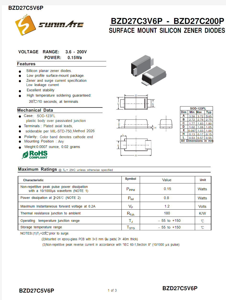
: SOD-123FL
plastic body over passivated junction Method 2026: Color band denotes cathode end : Any
Case Terminals Polarity Mounting Position : Plated axial leads,
solderable per MIL-STD-750,Mechanical Data
!!!!!!Weight:0.0007 ounce, 0.02 grams
3.58 3.72 0.55 0.57 0.530.15 0.17 0.13E D 1.00 1.03 0.097 1.05 1.08 1.021 1.80 1.83 1.77 2.75 2.78 2.72A 3.653 SOD-123FL
Dim Min Max Typ B C H L
All Dimensions in mm
BZD27C5V6P
BZD27C5V6P
BZD27C5V6P
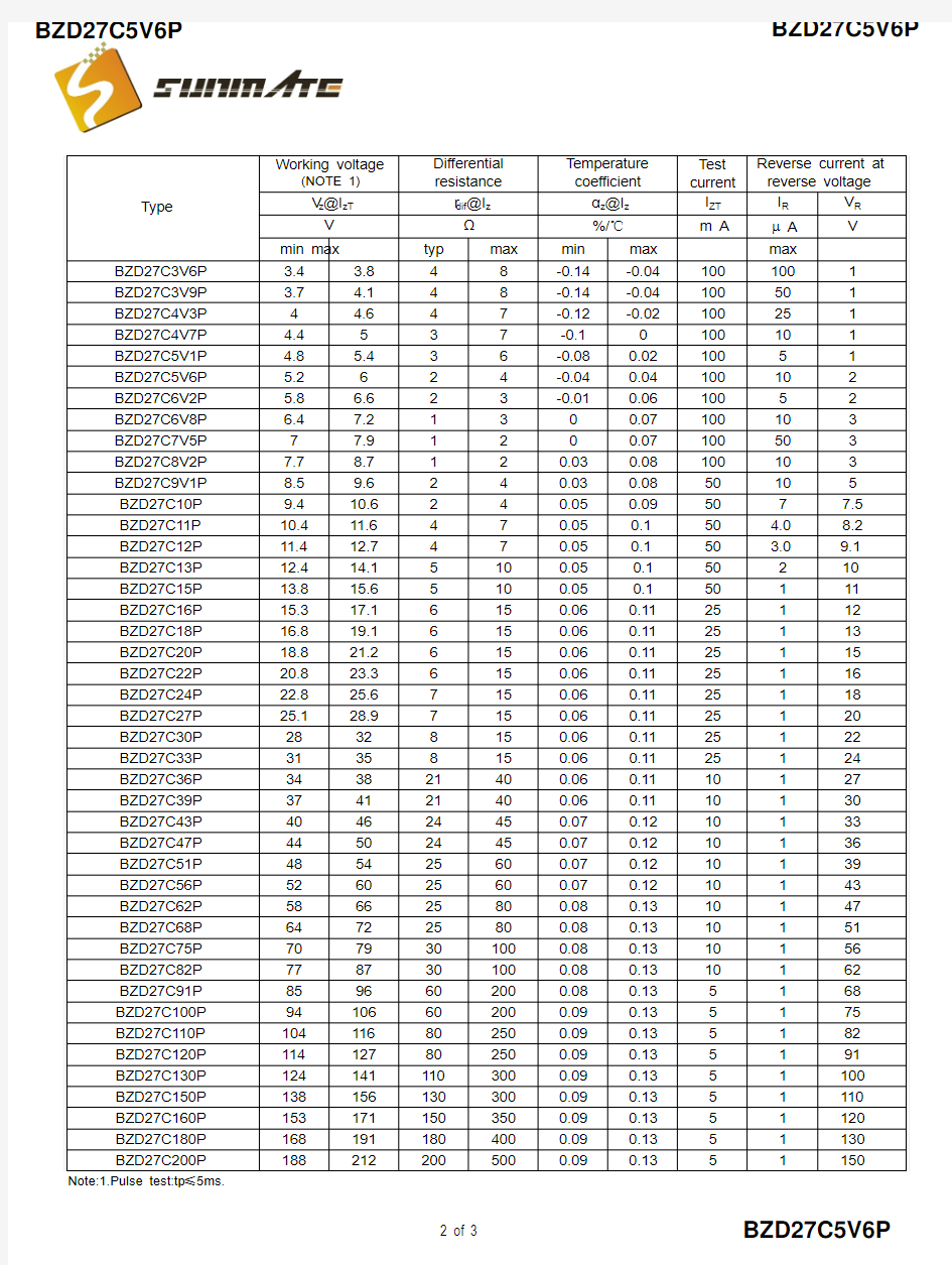
Type
Test
current
I ZT I R V R
m Aμ A V min max typ max min max max
Note:1.Pulse test:tp≤5ms.Working voltage
(NOTE 1)
V z@I zT
V
Differential
resistance
r dif@I z
?
Temperature
coefficient
αz@I z
%/℃
Reverse current at
reverse voltage
2 of 3
BZD27C3V6P 3.4 3.848-0.14-0.041001001
BZD27C3V9P 3.7 4.148-0.14-0.04100501
BZD27C4V3P4 4.647-0.12-0.02100251
BZD27C4V7P 4.4537-0.10100101
BZD27C5V1P 4.8 5.436-0.080.0210051
BZD27C5V6P 5.2624-0.040.04100102
BZD27C6V2P 5.8 6.623-0.010.0610052
BZD27C6V8P 6.47.21300.07100103
BZD27C7V5P77.91200.07100503
BZD27C8V2P7.78.7120.030.08100103
BZD27C9V1P8.59.6240.030.0850105
BZD27C10P9.410.6240.050.095077.5
BZD27C11P10.411.6470.050.150 4.08.2
BZD27C12P11.412.7470.050.150 3.09.1
BZD27C13P12.414.15100.050.150210
BZD27C15P13.815.65100.050.150111
BZD27C16P15.317.16150.060.1125112
BZD27C18P16.819.16150.060.1125113
BZD27C20P18.821.26150.060.1125115
BZD27C22P20.823.36150.060.1125116
BZD27C24P22.825.67150.060.1125118
BZD27C27P25.128.97150.060.1125120
BZD27C30P28328150.060.1125122
BZD27C33P31358150.060.1125124
BZD27C36P343821400.060.1110127
BZD27C39P374121400.060.1110130
BZD27C43P404624450.070.1210133
BZD27C47P445024450.070.1210136
BZD27C51P485425600.070.1210139
BZD27C56P526025600.070.1210143
BZD27C62P586625800.080.1310147
BZD27C68P647225800.080.1310151
BZD27C75P7079301000.080.1310156
BZD27C82P7787301000.080.1310162
BZD27C91P8596602000.080.135168
BZD27C100P94106602000.090.135175
BZD27C110P104116802500.090.135182
BZD27C120P114127802500.090.135191
BZD27C130P1241411103000.090.1351100
BZD27C150P1381561303000.090.1351110
BZD27C160P1531711503500.090.1351120
BZD27C180P1681911804000.090.1351130
BZD27C200P1882122005000.090.1351150 BZD27C5V6P BZD27C5V6P
BZD27C5V6P
Figure 1.Forward Currentvs.Forward Voltage
Figure 5.Power Dissipation vs.AmbientTemperature
F I – F o r w a r d C u r r e n t (A )
0.0
0.5 1.0 1.5 2.0 2.5 3.0
C – T y p . J u n c t i o n C a p a c i t a n c e ( p F )
D V R – Reverse Voltage (V)
0.0
0.51.01.52.02.53.00
255075100125150
T amb – Ambient T emperature ( q C )
P –P o w e r D i s s i p a t i o n ( W )
t o t Figure 2.Maximum Pulse Power Dissipation vs.Zener Voltage
Figure 4.Non-Repetitive Peak Reverse CurrentPulse Definition
020406080100120140
1600
25
50
75100125150175200V Znom – Zener Voltage ( V )
P –M a x . P u l s e P o w e r D i s s i p a t i o n ( W )R S M
I 3 of 3
BZD27C5V6P
BZD27C5V6P
BZD27C5V6P