PCB内层分割及覆铜
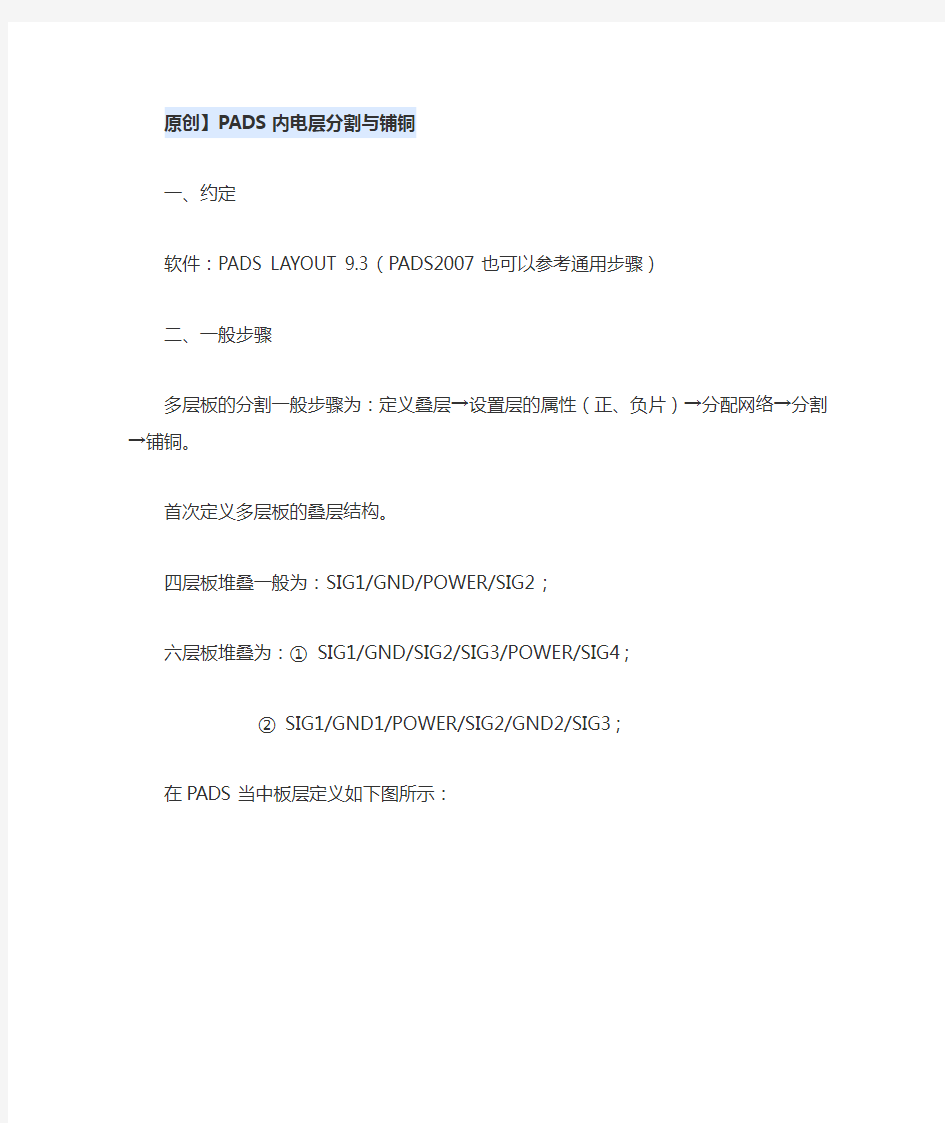
原创】PADS内电层分割与铺铜
一、约定
软件:PADS LAYOUT 9.3(PADS2007也可以参考通用步骤)
二、一般步骤
多层板的分割一般步骤为:定义叠层→设置层的属性(正、负片)→分配网络→分割→铺铜。首次定义多层板的叠层结构。
四层板堆叠一般为:SIG1/GND/POWER/SIG2;
六层板堆叠为:① SIG1/GND/SIG2/SIG3/POWER/SIG4;
② SIG1/GND1/POWER/SIG2/GND2/SIG3;
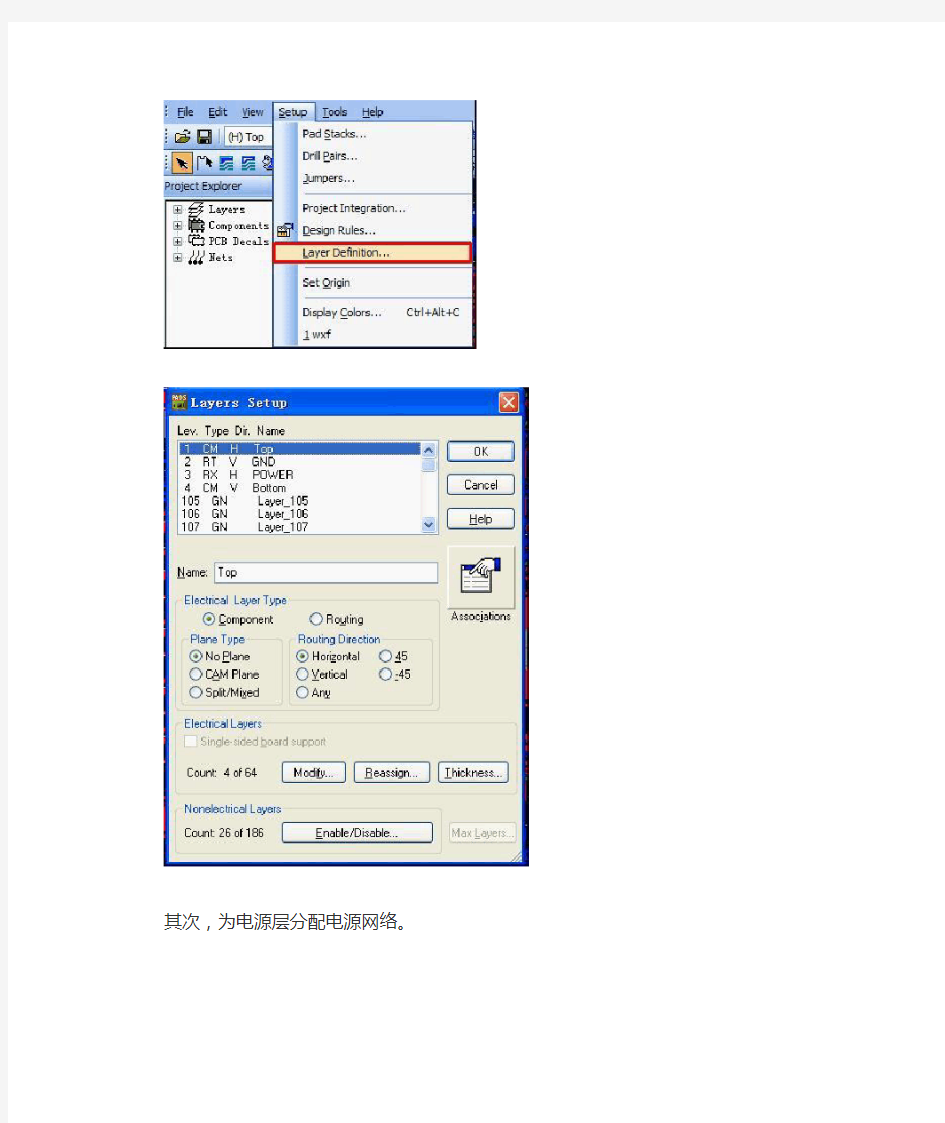
在PADS当中板层定义如下图所示:
其次,为电源层分配电源网络。
上图中强调一下“Plane Type”的问题。首先从工艺角度讲,内电层实物为薄薄的铜箔。在制造流程上有“正片”和“负片”之分。在PADS LAYOUT中,内电层属性配置当中,CAM PLANE为负片属性,其他两层为正片属性。以下部分是摘自PADS help文件:
· No Plane— Prevents planes from being added to the layer. The No Plane layer is available for rou ting. If you select No Plane, you can only create Copper and Copper Pour areas on the layer.
· CAM Plane— Sets the entire layer to be solid copper and connected to only one net. The CAM Pl ane layer is a negative image, and the copper does not appear in the design as it normally does for all other copper objects. You can not manipulate the shape/outline of the copper on this layer since it is generated automatically and covers the entire layer. This is an outmoded layer type. You can n
ot route traces on a CAM Plane layer. Copper Pours and Plane areas can not be created on CAM P lane layers.
· Split/Mixed Plane— Enables one or more planes on the layer, and enables routing on the layer. R outes can be placed within or without plane areas. Plane areas avoid traces within their outline by a clearance area defined in the design rules. Copper Pours can not be placed on Split/Mixed layers.
Plane areas are created on Split/Mixed plane layers and are similar to but more feature-packed tha n Copper Pours.
简单的讲,NO PLANE自由度更大一些,除了“Plane Area”以及相关的操作命令不能用以外,我们可以在NO PLANE层进行布线、铺铜、铺铜切割、2D图形边框的绘制等常用操作。
CAM Plane层只能赋予“单一网络”,可以是整片的电源也可以是地网络。在本层中,铜箔是以负片方式显示的。直观的讲,暗的区域实际为整片的铜箔,本层不能进行布线、铺铜和plane area操作。
Split/Mixed Plane是PADS专门针对多电源系统内电层分割给出的内电层属性。赋予该属性的内电层,只能通过“Plane area”命令以及“auto plane separate”命令进行电源层分割。
注意:电源层层属性的选择也可以选择为其他性质(如NO PLANE)。唯一需要注意的是,前期层属性的不同将导致后期铺铜方式的改变。否则就会发生无法铺铜或者铺铜错误的情况。
第三、分割操作。下文主要说明电源层为Split/Mixed Plane属性的情况。该属性下,分割操作使用
Auto plane separate命令。这里首先绘制铺铜的keepout层,这样可以防止每层的敷铜边界不一致的问题。利用Plane area命令依据PCB外框画出整体敷铜边框,完成后。右键选择“select shape”,双击选择该边框或者右键调用属性菜单。弹出以下菜单:
在Net assignment选项中分配一个最大的电源网络给当前内电层。然后点击进入“Options”菜单:
在这个菜单当中,这里我们可以设置过孔与铜皮的链接方式(热风焊盘或者是实焊盘)、选择铺铜的优先级。并且可以利用hatch grid与design grid的最小单位差值,进行网格铺铜。这里先不选择OK,退出当前菜单到PCB编辑界面。
接下来使用Auto plane separate命令进行分割。分割的原则:将目标网络的链接到本层的VIA全部圈起来。这里需要注意,不要形成闭合环状的电源分割区域(闭合的环形电场会产生电磁干扰,可以参考安培定则)。分割完成之后在另外一条边界上双击,弹出网络分配菜单。
根据高亮色区域选择对应的电源网络。依此类推,将所有需要分割的电源全部分割完毕之后,进入到铺铜阶段。
第四、内电层敷铜。这里内电层敷铜可以选择性敷铜,即可以给制定电源网络敷铜。也可以一次性全部敷铜。这里涉及到tools菜单下pour manager的操作。如下图所示:
点击Setup进入配置菜单:
铺铜管理器当中有三个选项卡:第一个Flood为全局铺铜命令。但是对plane area区域不适用。因为Flood Mode命令只对copper pour区域有效!
下面是flood和hatch的区别:
Flooding recalculates the pour area and recreates all clearances for the current obstacles within the pou r outline, observing clearance rules. Hatching refills (with hatch lines) existing pour polygons for the curr ent session; it does not recalculate the pour area. Each time you open a design file, you must flood or h atch the design; this information is not saved. In most cases, you can simply Hatch. Use Flood if you ma ke changes to the copper pour polygon that could create clearance violations or if you change clearance rules.
Flooding会重新计算灌注区域并重新计算当前填灌区域的外形线内障碍的所有间距,和一些注意的间距规则。Hatching则用来(用填充线)重新填充当前会话内已经存在的填灌多边形,而并不会重新计算填充填灌区域。每次打开一个设计文件时,你应当对这个设计进行flood或hatch;这些信息是不保存的。大部份情况下,你只要简单的Hatch一下就够了。当你对灌铜多边形的修改会引起规则冲突时,或当你修改了间距规则时,请使用flood。
总结。当进行到这一步的时候,分割和铺铜的工作就全部完成了。这里应该指出术语的准确性,flood copper 为灌铜,copper铺铜。这样可以准确的了解命令的意思,不会用错。此外,PADS默认是不保存flood和hatch敷铜效果的。每次打开之后需要用flood或者hatch命令进行敷铜或者填充操作。需要注意的是,针对内电层使用了Split/Mixed Plane属性,flood和hatch命令不起作用,依然是在每次打开的时候使用pour manager中的“Plane connect”操作,可以一次性全部给内电层敷铜。
PS:内电敷铜也可以通过选择边框的方式,使用flood命令来敷铜。前提是关闭pour outline显示模式并点选pour outline进行删除操作,然后再flood。否则提示无法灌铜。由于容易出错,还是选择plane connect 操作安全。