LM4890规格书pdf
LM4890
1Watt Audio Power Amplifier
General Description
The LM4890is an audio power amplifier primarily designed for demanding applications in mobile phones and other por-table communication device applications.It is capable of delivering 1watt of continuous average power to an 8?BTL load with less than 1%distortion (THD+N)from a 5V DC power supply.
Boomer audio power amplifiers were designed specifically to provide high quality output power with a minimal amount of external components.The LM4890does not require output coupling capacitors or bootstrap capacitors,and therefore is ideally suited for mobile phone and other low voltage appli-cations where minimal power consumption is a primary re-quirement.
The LM4890features a low-power consumption shutdown mode,which is achieved by driving the shutdown pin with logic low.Additionally,the LM4890features an internal ther-mal shutdown protection mechanism.
The LM4890contains advanced pop &click circuitry which eliminates noises which would otherwise occur during turn-on and turn-off transitions.
The LM4890is unity-gain stable and can be configured by external gain-setting resistors.
Key Specifications
j PSRR at 217Hz,V DD =5V (Fig.1)62dB(typ.)j Power Output at 5.0V &1%THD 1W(typ.)j Power Output at 3.3V &1%THD 400mW(typ.)j Shutdown Current
0.1μA(typ.)
Features
n Available in space-saving packages:micro SMD,MSOP ,SOIC,and LLP
n Ultra low current shutdown mode
n BTL output can drive capacitive loads
n Improved pop &click circuitry eliminates noises during turn-on and turn-off transitions n 2.2-5.5V operation
n No output coupling capacitors,snubber networks or bootstrap capacitors required n Thermal shutdown protection n Unity-gain stable
n External gain configuration capability
Applications
n Mobile Phones n PDAs
n Portable electronic devices
Connection Diagrams
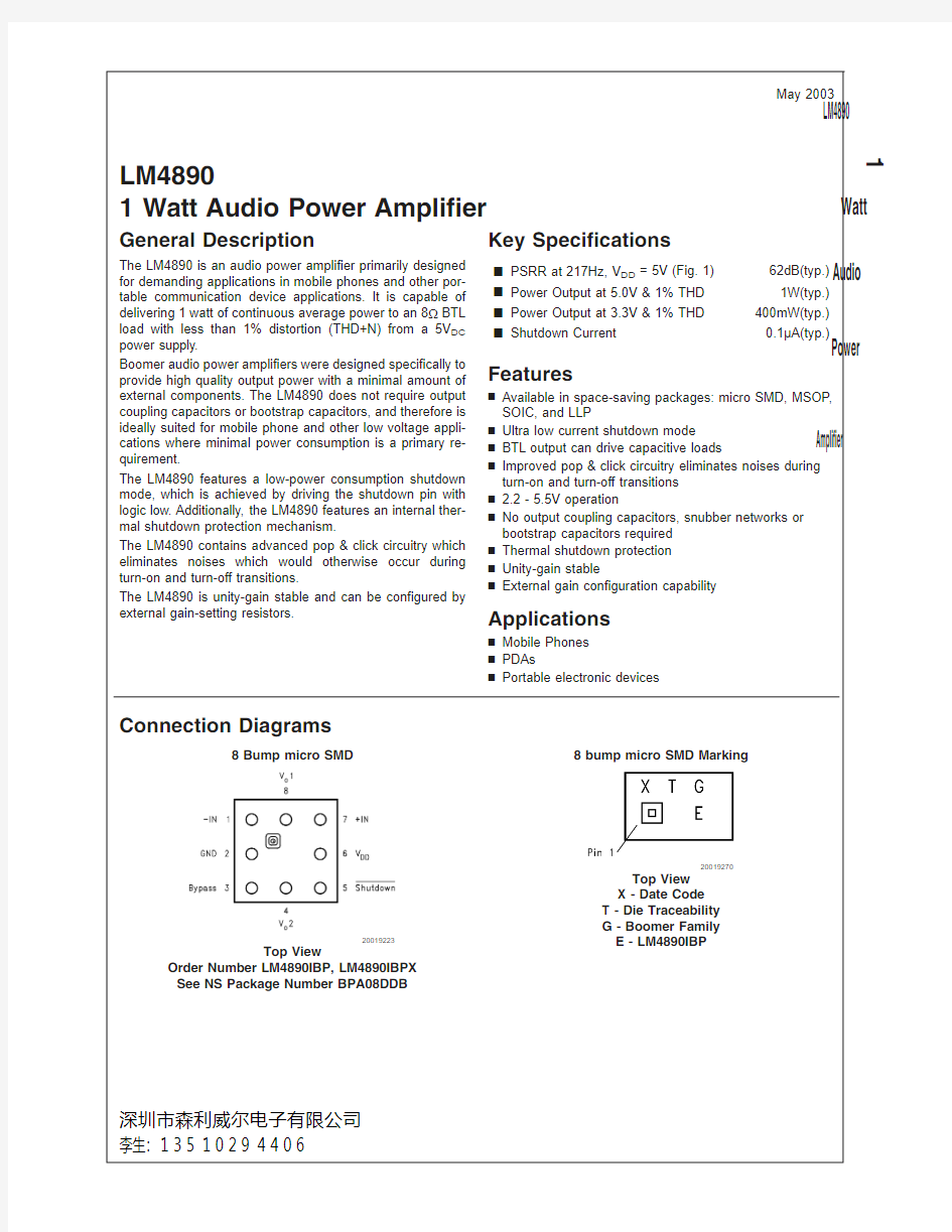
8Bump micro SMD
8bump micro SMD Marking
20019223
Top View
Order Number LM4890IBP,LM4890IBPX See NS Package Number BPA08DDB
20019270
Top View X -Date Code T -Die Traceability G -Boomer Family E -LM4890IBP
May 2003
LM48901Watt Audio Power Amplifier
深圳市森利威尔电子有限公司李生:135 1029 4406
Connection Diagrams
(Continued)
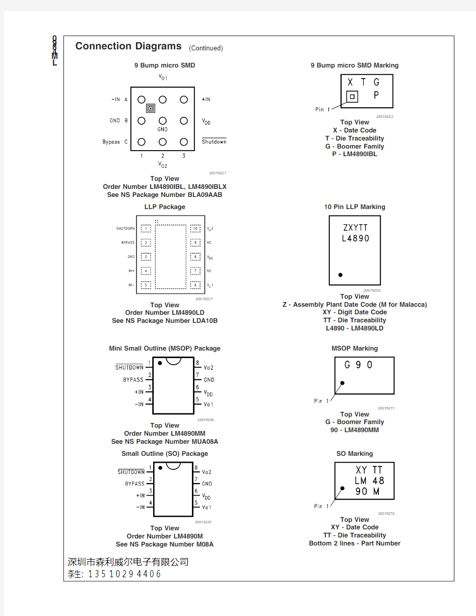
9Bump micro SMD
9Bump micro SMD Marking
200192C1
Top View
Order Number LM4890IBL,LM4890IBLX See NS Package Number BLA09AAB
200192C2
Top View X -Date Code T -Die Traceability G -Boomer Family P -LM4890IBL
LLP Package
10Pin LLP Marking
200192C7
Top View
Order Number LM4890LD
See NS Package Number LDA10B
200192C6
Top View
Z -Assembly Plant Date Code (M for Malacca)
XY -Digit Date Code TT -Die Traceability L4890-LM4890LD
Mini Small Outline (MSOP)Package
MSOP Marking
20019236
Top View
Order Number LM4890MM See NS Package Number MUA08A
20019271
Top View
G -Boomer Family 90-LM4890MM
Small Outline (SO)Package
SO Marking
20019235
Top View
Order Number LM4890M See NS Package Number M08A
20019272
Top View XY -Date Code TT -Die Traceability
Bottom 2lines -Part Number
L M 4890
深圳市森利威尔电子有限公司李生:135 1029 4406
Connection Diagrams(Continued)
9Bump micro SMD9Bump micro SMD Marking
200192C1
Top View
Order Number LM4890ITL,LM4890ITLX
See NS Package Number TLA09AAA
200192D0
Top View
X-Date Code
T-Die Traceability
G-Boomer Family
A8-LM4890ITL
Typical Application
20019201
FIGURE1.Typical Audio Amplifier Application Circuit
LM4890
3
深圳市森利威尔电子有限公司
李生:135 1029 4406
Absolute Maximum Ratings
(Note 2)
If Military/Aerospace specified devices are required,please contact the National Semiconductor Sales Office/Distributors for availability and specifications.Supply Voltage (Note 11) 6.0V
Storage Temperature ?65?C to +150?C Input Voltage
?0.3V to V DD +0.3V Power Dissipation (Note 3)Internally Limited
ESD Susceptibility (Note 4)2000V Junction Temperature 150?C
Thermal Resistance θJC (SOP)35?C/W θJA (SOP)
150?C/W θJA (8Bump micro SMD,Note 12)
220?C/W
θJA (9Bump micro SMD,Note 12)180?C/W θJC (MSOP)56?C/W θJA (MSOP)190?C/W θJA (LLP)
220?C/W
Soldering Information
See AN-1112"microSMD Wafers Level Chip Scale Package."
See AN-1187"Leadless Leadframe Package (LLP)."
Operating Ratings
Temperature Range T MIN ≤T A ≤T MAX ?40?C ≤T A ≤85?C Supply Voltage
2.2V ≤V DD ≤5.5V
Electrical Characteristics V DD =5V
(Notes 1,2,8)
The following specifications apply for the circuit shown in Figure 1unless otherwise specified.Limits apply for T A =25?C.
Symbol Parameter
Conditions
LM4890
Units (Limits)Typical Limit (Note 6)
(Notes 7,9)
I DD Quiescent Power Supply Current V IN =0V,I o =0A,No Load 48mA (max)V IN =0V,I o =0A,8?Load 510mA (max)I SD Shutdown Current
V SHUTDOWN =0V
0.1
2.0μA (max)V SDIH Shutdown Voltage Input High 1.2V (min)V SDIL Shutdown Voltage Input Low 0.4V (max)V OS
Output Ofsett Voltage
750mV (max)R OUT-GND Resistor Output to GND (Note 10)8.5
9.7k ?(max)7.0k ?(min)P o Output Power (8?)THD =2%(max);f =1kHz
1.00.8W T WU Wake-up time
170220ms (max)T SD Thermal Shutdown Temperature 170
150?C (min)190
?C (max)
THD+N Total Harmonic Distortion+Noise P o =0.4Wrms;f =1kHz
0.1%PSRR
Power Supply Rejection Ratio (Note 14)V ripple =200mV sine p-p
Input Terminated with 10ohms to ground 62(f =217Hz)66(f =1kHz)
55
dB (min)
T SDT
Shut Down Time
8?load
1.0
ms (max)
Electrical Characteristics V DD =3V
(Notes 1,2,8)
The following specifications apply for the circuit shown in Figure 1unless otherwise specified.Limits apply for T A =25?C.
Symbol Parameter
Conditions
LM4890
Units (Limits)Typical Limit (Note 6)(Notes 7,9)
I DD Quiescent Power Supply Current V IN =0V,I o =0A,No Load 3.57mA (max)V IN =0V,I o =0A,8?Load 4.59mA (max)I SD Shutdown Current
V SHUTDOWN =0V
0.1
2.0μA (max)V SDIH Shutdown Voltage Input High 1.2V(min)V SDIL Shutdown Voltage Input Low 0.4V(max)V OS
Output Offset Voltage
750mV (max)R OUT-GND Resistor Output to Gnd (Note 10)8.59.7k ?(max)7.0k ?(min)T WU
Wake-up time
120
180
ms (max)
L M 4890
深圳市森利威尔电子有限公司李生:135 1029 4406
Electrical Characteristics V DD =3V (Notes 1,2,8)
The following specifications apply for the circuit shown in Figure 1unless otherwise specified.Limits apply for T A =25?C.(Continued)
Symbol Parameter
Conditions
LM4890
Units (Limits)Typical Limit (Note 6)(Notes 7,9)
P o Output Power (8?)
THD =1%(max);f =1kHz
0.310.28W T SD Thermal Shutdown Temperature 170150?C(min)190
?C(max)THD+N Total Harmonic Distortion+Noise P o =0.15Wrms;f =1kHz 0.1%PSRR
Power Supply Rejection Ratio (Note 14)
V ripple =200mV sine p-p
Input terminated with 10ohms to ground
56(f =217Hz)62(f =1kHz)
45dB(min)
Electrical Characteristics V DD =2.6V
(Notes 1,2,8)
The following specifications apply for for the circuit shown in Figure 1unless otherwise specified.Limits apply for T A =25?C.
Symbol Parameter
Conditions
LM4890
Units (Limits)Typical Limit (Note 6)(Notes 7,9)
I DD Quiescent Power Supply Current V IN =0V,I o =0A,No Load 2.6mA (max)I SD Shutdown Current V SHUTDOWN =0V
0.1μA (max)
P 0Output Power (8?)Output Power (4?)
THD =1%(max);f =1kHz THD =1%(max);f =1kHz 0.20.22W W THD+N Total Harmonic Distortion+Noise P o =0.1Wrms;f =1kHz
0.08%PSRR
Power Supply Rejection Ratio (Note 14)
V ripple =200mV sine p-p
Input Terminated with 10ohms to ground
44(f =217Hz)44(f =1kHz)
dB
Note 1:All voltages are measured with respect to the ground pin,unless otherwise specified.
Note 2:Absolute Maximum Ratings indicate limits beyond which damage to the device may occur.Operating Ratings indicate conditions for which the device is functional,but do not guarantee specific performance limits.Electrical Characteristics state DC and AC electrical specifications under particular test conditions which guarantee specific performance limits.This assumes that the device is within the Operating Ratings.Specifications are not guaranteed for parameters where no limit is given,however,the typical value is a good indication of device performance.
Note 3:The maximum power dissipation must be derated at elevated temperatures and is dictated by T JMAX ,θJA ,and the ambient temperature T A .The maximum allowable power dissipation is P DMAX =(T JMAX –T A )/θJA or the number given in Absolute Maximum Ratings,whichever is lower.For the LM4890,see power derating curves for additional information.
Note 4:Human body model,100pF discharged through a 1.5k ?resistor.Note 5:Machine Model,220pF–240pF discharged through all pins.Note 6:Typicals are measured at 25?C and represent the parametric norm.
Note 7:Limits are guaranteed to National’s AOQL (Average Outgoing Quality Level).
Note 8:For micro SMD only,shutdown current is measured in a Normal Room Environment.Exposure to direct sunlight will increase I SD by a maximum of 2μA.Note 9:Datasheet min/max specification limits are guaranteed by design,test,or statistical analysis.
Note 10:ROUT is measured from each of the output pins to ground.This value represents the parallel combination of the 10k ohm output resistors and the two 20k ohm resistors.
Note 11:If the product is in shutdown mode and V DD exceeds 6V (to a max of 8V V DD ),then most of the excess current will flow through the ESD protection circuits.If the source impedance limits the current to a max of 10ma,then the part will be protected.If the part is enabled when V DD is greater than 5.5V and less than 6.5V,no damage will occur,although operational life will be reduced.Operation above 6.5V with no current limit will result in permanent damage.
Note 12:All bumps have the same thermal resistance and contribute equally when used to lower thermal resistance.All bumps must be connected to achieve specified thermal resistance.
Note 13:Maximum power dissipation (P DMAX )in the device occurs at an output power level significantly below full output power.P DMAX can be calculated using Equation 1shown in the Application section.It may also be obtained from the power dissipation graphs.
Note 14:PSRR is a function of system gain.Specifications apply to the circuit in Figure 1where A V =2.Higher system gains will reduce PSRR value by the amount of gain increase.A system gain of 10represents a gain increase of 14dB.PSRR will be reduced by 14dB and applies to all operating voltages.
LM4890
5
深圳市森利威尔电子有限公司李生:135 1029 4406
External Components Description
(Figure 1)
Components Functional Description
1.R IN Inverting input resistance which sets the closed-loop gain in conjunction with R f .This resistor also forms a high pass filter with C IN at f C =1/(2πR IN C IN ).
2.
C IN
Input coupling capacitor which blocks the DC voltage at the amplifier’s input terminals.Also creates a highpass filter with R IN at f c =1/(2πR IN C IN ).Refer to the section,Proper Selection of External Components ,for an explanation of how to determine the value of C IN .3.R f Feedback resistance which sets the closed-loop gain in conjunction with R IN .
4.
C S
Supply bypass capacitor which provides power supply filtering.Refer to the section,Power Supply Bypassing ,for information concerning proper placement and selection of the supply bypass capacitor,C BYPASS .
5.
C BYPASS Bypass pin capacitor which provides half-supply filtering.Refer to the section,Proper Selection of External
Components ,for information concerning proper placement and selection of C BYPASS .
L M 4890
深圳市森利威尔电子有限公司李生:135 1029 4406
Typical Performance Characteristics
THD+N vs Frequency
at V DD =5V,8?R L ,and PWR =250mW,A V =2
THD+N vs Frequency
at V DD =3.3V,8?R L ,and PWR =150mW,A V =2
2001923720019238
THD+N vs Frequency
at V DD
=3V,R L =8?,PWR =250mW,A V =2
20019290
THD+N vs Frequency
@V DD
=2.6V,R L =8?,PWR =100mW,A V =2
THD+N vs Frequency
@V DD
=2.6V,R L =4?,PWR =100mW,A V =2
2001923920019240
LM4890
7
深圳市森利威尔电子有限公司李生:135 1029 4406
Typical Performance Characteristics
(Continued)
THD+N vs Power Out
@V DD =5V,R L =8?,1kHz,A V =2
THD+N vs Power Out
@V DD =3.3V,R L =8?,1kHz,A V =2
200192C920019242
THD+N vs Power Out
@V DD =3V,R L =8?,1kHz,A V =2
20019291
THD+N vs Power Out
@V DD
=2.6V,R L =8?,1kHz,A V =2
THD+N vs Power Out
@V DD
=2.6V,R L =4?,1kHz,A V =2
2001924320019244
L M 4890
深圳市森利威尔电子有限公司李生:135 1029 4406
Typical Performance Characteristics
(Continued)
Power Supply Rejection Ratio (PSRR)@A V =2
V DD =5V,V ripple =200mvp-p
R L =8?,R IN =10?
Power Supply Rejection Ratio (PSRR)@A V =2
V DD =5V,V ripple =200mvp-p
R L =8?,R IN =Float
2001924520019273
Power Supply Rejection Ratio (PSRR)@A V =4
V DD =5V,V ripple =200mvp-p
R L =8?,R IN =10?Power Supply Rejection Ratio (PSRR)@A V =4
V DD =5V,V ripple =200mvp-p
R L =8?,R IN =Float
200192A9200192B8
LM4890
9
深圳市森利威尔电子有限公司李生:135 1029 4406
Typical Performance Characteristics
(Continued)
Power Supply Rejection Ratio (PSRR)@A V =2
V DD =3V,V ripple =200mvp-p,
R L =8?,R IN =10?
Power Supply Rejection Ratio (PSRR)@A V =2
V DD =3V,V ripple =200mvp-p,
R L =8?,R IN =Float
200192C5
20019293
Power Supply Rejection Ratio (PSRR)@A V =4
V DD =3V,V ripple =200mvp-p,
R L =8?,R IN =10?Power Supply Rejection Ratio (PSRR)@A V =4
V DD =3V,V ripple =200mvp-p,
R L =8?,R IN =Float
200192B1200192B9
Power Supply Rejection Ratio (PSRR)@A V =2
V DD =3.3V,V ripple =200mvp-p,
R L =8?,R IN =10?Power Supply Rejection Ratio (PSRR)@A V =2
V DD =2.6V,V ripple =200mvp-p,
R L =8?,R IN =10?
2001924620019247
L M 4890
深圳市森利威尔电子有限公司李生:135 1029 4406
Typical Performance Characteristics
(Continued)
PSRR vs DC Output Voltage
V DD =5V,A V =2
PSRR vs DC Output Voltage
V DD =5V,A V =4
20019296
20019297
PSRR vs DC Output Voltage
V DD =5V,A V =10PSRR vs DC Output Voltage
V DD =3V,A V =2
200192A3
20019294
PSRR vs DC Output Voltage
V DD =3V,A V =4PSRR vs DC Output Voltage
V DD =3V,A V =10
20019295200192A4
LM4890
11
深圳市森利威尔电子有限公司李生:135 1029 4406
Typical Performance Characteristics
(Continued)
PSRR Distribution V DD =5V
217Hz,200mvp-p,-30,+25,and +80?C
PSRR Distribution V DD =3V
217Hz,200mvp-p,-30,+25,and +80?C
200192B4
200192B5
Power Supply Rejection Ration vs
Bypass Capacitor Size
V DD
=5V,Input Grounded =10?,Output Load =8?
Power Supply Rejection Ration vs
Bypass Capacitor Size
V DD
=3V,Input Grounded =10?,Output Load =8?
200192A7Top Trace =No Cap,Next Trace Down =1μf Next Trace Down =2μf,Bottom Trace =4.7μf 200192A8
Top Trace =No Cap,Next Trace Down =1μf Next Trace Down =2μf,Bottom Trace =4.7μf LM4890vs LM4877Power Supply Rejection Ratio
V DD =5V,Input Grounded =10?Output Load =8?,200mV Ripple
LM4890vs LM4877Power Supply Rejection Ratio
V DD =3V,Input Grounded =10?Output Load =8?,200mV Ripple
20019288LM4890=Bottom Trace LM4877=Top Trace 20019289
LM4890=Bottom Trace LM4877=Top Trace
L M 4890
深圳市森利威尔电子有限公司李生:135 1029 4406
Typical Performance Characteristics
(Continued)
Power Derating Curves (P DMAX =670mW)
Power Derating -8bump μSMD (P DMAX =670mW)
20019283Ambient Temperature in Degrees C Note:(P DMAX =670mW for 5V,8?)
20019284
Ambient Temperature in Degrees C Note:(P DMAX =670mW for 5V,8?)
Power Derating -9bump μSMD (P DMAX =670mW)
Power Derating -10Pin LD Pkg (P DMAX =670mW)
20019285
Ambient Temperature in Degrees C Note:(P DMAX =670mW for 5V,8?)200192C8
Ambient Temperature in Degrees C Note:(P DMAX =670mW for 5V,8?)Power Output vs Supply Voltage
Power Output vs Temperature
200192A1200192A2
LM4890
13
深圳市森利威尔电子有限公司李生:135 1029 4406
Typical Performance Characteristics
(Continued)
Power Dissipation vs Output Power V DD =5V,1kHz,8?,THD ≤1.0%
Power Dissipation vs Output Power V DD =3.3V,1kHz,8?,THD ≤1.0%
2001924820019249
Power Dissipation vs Output Power
V DD =2.6V,1kHz
Output Power vs Load Resistance
2001925020019274
Supply Current
vs Ambient Temperature Clipping (Dropout)Voltage
vs Supply Voltage
2001929920019252
L M 4890
深圳市森利威尔电子有限公司李生:135 1029 4406
Typical Performance Characteristics
(Continued)
Max Die Temp
at P DMAX (9bump microSMD)
Max Die Temp
at P DMAX (8bump microSMD)
2001928620019287
Output Offset Voltage
Supply Current vs Shutdown Voltage
200192B720019253
Shutdown Hysterisis Voltage
V DD =5V Shutdown Hysterisis Voltage
V DD =3V
2001927920019280
LM4890
15
深圳市森利威尔电子有限公司李生:135 1029 4406
Typical Performance Characteristics
(Continued)
Open Loop Frequency Response
V DD =5V,No Load
Open Loop Frequency Response
V DD =3V,No Load
2001928120019282
Gain /Phase Response,A V =2V DD =5V,8?Load,C LOAD =500pF Gain /Phase Response,A V =4V DD =5V,8?Load,C LOAD =500pF
200192B2200192B3
Phase Margin vs C LOAD ,A V =2
V DD =5V,8?Load
Capacitance to gnd on each output Phase Margin vs C LOAD ,A V =4
V DD =5V,8?Load
Capacitance to gnd on each output
200192A5200192A6
L M 4890
深圳市森利威尔电子有限公司李生:135 1029 4406
Typical Performance Characteristics
(Continued)
Phase Margin and Limits
vs Application Variables,R IN =22K ?
20019298
Wake Up Time (T WU )
200192B6
Frequency Response vs Input Capacitor Size
Noise Floor
2001925420019256
LM4890
17
Application Information
BRIDGED CONFIGURATION EXPLANATION
As shown in Figure 1,the LM4890has two operational amplifiers internally,allowing for a few different amplifier configurations.The first amplifier’s gain is externally config-urable,while the second amplifier is internally fixed in a unity-gain,inverting configuration.The closed-loop gain of the first amplifier is set by selecting the ratio of R f to R IN while the second amplifier’s gain is fixed by the two internal 20k ?resistors.Figure 1shows that the output of amplifier one serves as the input to amplifier two which results in both amplifiers producing signals identical in magnitude,but out of phase by 180?.Consequently,the differential gain for the IC is
A VD =2*(R f /R IN )
By driving the load differentially through outputs Vo1and Vo2,an amplifier configuration commonly referred to as “bridged mode”is established.Bridged mode operation is different from the classical single-ended amplifier configura-tion where one side of the load is connected to ground.A bridge amplifier design has a few distinct advantages over the single-ended configuration,as it provides differential drive to the load,thus doubling output swing for a specified supply voltage.Four times the output power is possible as compared to a single-ended amplifier under the same con-ditions.This increase in attainable output power assumes that the amplifier is not current limited or clipped.In order to choose an amplifier’s closed-loop gain without causing ex-cessive clipping,please refer to the Audio Power Amplifier Design section.
A bridge configuration,such as the one used in the LM4890,also creates a second advantage over single-ended amplifi-ers.Since the differential outputs,Vo1and Vo2,are biased at half-supply,no net DC voltage exists across the load.This eliminates the need for an output coupling capacitor which is required in a single supply,single-ended amplifier configura-tion.Without an output coupling capacitor,the half-supply bias across the load would result in both increased internal IC power dissipation and also possible loudspeaker damage.EXPOSED-DAP PACKAGE PC
B MOUNTING CONSIDERATIONS FOR THE LM4890LD
The LM4890LD’s exposed-DAP (die attach paddle)package (LD)provides a low thermal resistance between the die and the PCB to which the part is mounted and soldered.The LM4890LD package should have its DAP soldered to the grounded copper pad (heatsink)under the LM4890LD (the NC pins,no connect,and ground pins should also be directly connected to this copper pad-heatsink area).The area of the copper pad (heatsink)can be determined from the LD Power Derating graph.If the multiple layer copper heatsink areas are used,then these inner layer or backside copper heatsink areas should be connected to each other with 4(2x 2)vias.The diameter for these vias should be between 0.013inches and 0.02inches with a 0.050inch pitch-spacing.Ensure efficient thermal conductivity by plating through and solder-filling the vias.Further detailed information concerning PCB layout,fabrication,and mounting an LLP package is avail-able from National Semiconductor’s Package Engineering Group under application note AN1187.
POWER DISSIPATION
Power dissipation is a major concern when designing a successful amplifier,whether the amplifier is bridged or single-ended.A direct consequence of the increased power delivered to the load by a bridge amplifier is an increase in internal power dissipation.Since the LM4890has two opera-tional amplifiers in one package,the maximum internal power dissipation is 4times that of a single-ended amplifier.The maximum power dissipation for a given application can be derived from the power dissipation graphs or from Equa-tion 1.
P DMAX =4*(V DD )2/(2π2R L )
(1)It is critical that the maximum junction temperature T JMAX of 150?C is not exceeded.T JMAX can be determined from the power derating curves by using P DMAX and the PC board foil area.By adding additional copper foil,the thermal resistance of the application can be reduced,resulting in higher P DMAX .Additional copper foil can be added to any of the leads connected to the LM4890.Refer to the APPLICATION IN-FORMATION on the LM4890reference design board for an example of good heat sinking.If T JMAX still exceeds 150?C,then additional changes must be made.These changes can include reduced supply voltage,higher load impedance,or reduced ambient temperature.Internal power dissipation is a function of output power.Refer to the Typical Performance Characteristics curves for power dissipation information for different output powers and output loading.
POWER SUPPLY BYPASSING
As with any amplifier,proper supply bypassing is critical for low noise performance and high power supply rejection.The capacitor location on both the bypass and power supply pins should be as close to the device as possible.Typical appli-cations employ a 5V regulator with 10μF tantalum or elec-trolytic capacitor and a ceramic bypass capacitor which aid in supply stability.This does not eliminate the need for bypassing the supply nodes of the LM4890.The selection of a bypass capacitor,especially C BYPASS ,is dependent upon PSRR requirements,click and pop performance (as ex-plained in the section,Proper Selection of External Com-ponents ),system cost,and size constraints.
SHUTDOWN FUNCTION
In order to reduce power consumption while not in use,the LM4890contains a shutdown pin to externally turn off the amplifier’s bias circuitry.This shutdown feature turns the amplifier off when a logic low is placed on the shutdown pin.By switching the shutdown pin to ground,the LM4890supply current draw will be minimized in idle mode.While the device will be disabled with shutdown pin voltages less than 0.5V DC ,the idle current may be greater than the typical value of 0.1μA.(Idle current is measured with the shutdown pin grounded).
In many applications,a microcontroller or microprocessor output is used to control the shutdown circuitry to provide a quick,smooth transition into shutdown.Another solution is to use a single-pole,single-throw switch in conjunction with an external pull-up resistor.When the switch is closed,the shutdown pin is connected to ground and disables the am-plifier.If the switch is open,then the external pull-up resistor will enable the LM4890.This scheme guarantees that the shutdown pin will not float thus preventing unwanted state changes.
L M 4890
Application Information
(Continued)
SHUTDOWN OUTPUT IMPEDANCE For R f =20k ohms:
Z OUT1(between Out1and GND)=10k||50k||R f =6k ?Z OUT2(between Out2and GND)=10k||(40k+(10k||R f ))=8.3k ?
Z OUT1-2(between Out1and Out2)=40k||(10k+(10k||R f ))=11.7k ?
The -3dB roll off for these measurements is 600kHz PROPER SELECTION OF EXTERNAL COMPONENTS Proper selection of external components in applications us-ing integrated power amplifiers is critical to optimize device and system performance.While the LM4890is tolerant of external component combinations,consideration to compo-nent values must be used to maximize overall system qual-ity.
The LM4890is unity-gain stable which gives the designer maximum system flexibility.The LM4890should be used in low gain configurations to minimize THD+N values,and maximize the signal to noise ratio.Low gain configurations require large input signals to obtain a given output power.Input signals equal to or greater than 1Vrms are available from sources such as audio codecs.Please refer to the section,Audio Power Amplifier Design ,for a more com-plete explanation of proper gain selection.
Besides gain,one of the major considerations is the closed-loop bandwidth of the amplifier.To a large extent,the band-width is dictated by the choice of external components shown in Figure 1.The input coupling capacitor,C IN ,forms a first order high pass filter which limits low frequency re-sponse.This value should be chosen based on needed frequency response for a few distinct reasons.
Selection Of Input Capacitor Size
Large input capacitors are both expensive and space hungry for portable designs.Clearly,a certain sized capacitor is needed to couple in low frequencies without severe attenu-ation.But in many cases the speakers used in portable systems,whether internal or external,have little ability to reproduce signals below 100Hz to 150Hz.Thus,using a large input capacitor may not increase actual system perfor-mance.
In addition to system cost and size,click and pop perfor-mance is effected by the size of the input coupling capacitor,C IN .A larger input coupling capacitor requires more charge to reach its quiescent DC voltage (nominally 1/2V DD ).This charge comes from the output via the feedback and is apt to create pops upon device enable.Thus,by minimizing the capacitor size based on necessary low frequency response,turn-on pops can be minimized.
Besides minimizing the input capacitor size,careful consid-eration should be paid to the bypass capacitor value.Bypass capacitor,C BYPASS ,is the most critical component to mini-mize turn-on pops since it determines how fast the LM4890turns on.The slower the LM4890’s outputs ramp to their quiescent DC voltage (nominally 1/2V DD ),the smaller the turn-on pop.Choosing C BYPASS equal to 1.0μF along with a small value of C IN ,(in the range of 0.1μF to 0.39μF),should
produce a virtually clickless and popless shutdown function.While the device will function properly,(no oscillations or motorboating),with C BYPASS equal to 0.1μF,the device will be much more susceptible to turn-on clicks and pops.Thus,a value of C BYPASS equal to 1.0μF is recommended in all but the most cost sensitive designs.AUDIO POWER AMPLIFIER DESIGN A 1W/8?AUDIO AMPLIFIER Given:
Power Output 1Wrms
Load Impedance 8?Input Level 1Vrms Input Impedance 20k ?
Bandwidth
100Hz–20kHz ±0.25dB
A designer must first determine the minimum supply rail to obtain the specified output power.By extrapolating from the Output Power vs Supply Voltage graphs in the Typical Per-formance Characteristics section,the supply rail can be easily found.A second way to determine the minimum sup-ply rail is to calculate the required V opeak using Equation 2and add the output https://www.360docs.net/doc/8810252195.html,ing this method,the minimum supply voltage would be (V opeak +(V OD TOP +V OD BOT )),where V OD BOT and V OD TOP are extrapolated from the Dropout Volt-age vs Supply Voltage curve in the Typical Performance Characteristics section.
(2)
5V is a standard voltage which in most applications is cho-sen for the supply rail.Extra supply voltage creates head-room that allows the LM4890to reproduce peaks in excess of 1W without producing audible distortion.At this time,the designer must make sure that the power supply choice along with the output impedance does not violate the conditions explained in the Power Dissipation section.
Once the power dissipation equations have been addressed,the required differential gain can be determined from Equa-tion 3.
(3)
R f /R IN =A VD /2
From Equation 3,the minimum A VD is 2.83;use A VD =3.Since the desired input impedance is 20k ?,and with an A VD gain of 3,a ratio of 1.5:1of R f to R IN results in an allocation of R IN =20k ?and R f =30k ?.The final design step is to address the bandwidth requirements which must be stated as a pair of ?3dB frequency points.Five times away from a ?3dB point is 0.17dB down from passband response which is better than the required ±0.25dB specified.
f L =100Hz/5=20Hz f H =20kHz *5=100kHz
LM4890
19
Application Information
(Continued)
As stated in the External Components section,R IN in con-junction with C IN create a highpass filter.
C IN ≥1/(2π*20k ?*20Hz)=0.397μF;use 0.39μF The high frequency pole is determined by the product of the desired frequency pole,f H ,and the differential gain,A V
D .
With a A VD =3and f H =100kHz,the resulting GBWP =300kHz which is much smaller than the LM4890GBWP of 2.5MHz.This calculation shows that if a designer has a need to design an amplifier with a higher differential gain,the LM4890can still be used without running into bandwidth limitations.
The LM4890is unity-gain stable and requires no external components besides gain-setting resistors,an input coupling capacitor,and proper supply bypassing in the typical appli-cation.However,if a closed-loop differential gain of greater than 10is required,a feedback capacitor (C4)may be needed as shown in Figure 2to bandwidth limit the amplifier.This feedback capacitor creates a low pass filter that elimi-nates possible high frequency oscillations.Care should be taken when calculating the -3dB frequency in that an incor-rect combination of R 3and C 4will cause rolloff before 20kHz.A typical combination of feedback resistor and ca-pacitor that will not produce audio band high frequency rolloff is R 3=20k ?and C 4=25pf.These components result in a -3dB point of approximately 320kHz.
HIGHER GAIN AUDIO AMPLIFIER
20019224
FIGURE 2.
L M 4890
锂电池规格书
储能型磷酸铁锂电池规格书STORAGE LiFePO4 BATTERY SPECIFICATIONS 客户名称(Customer): 产品型号(Type): CF12V80Ah 发行日期(Issuing Date):
1. 适用范围(Product Scope) 本规格书描述了锂离子二次电池的技术要求、测量方法、运输、储存及注意事项。 This Specification describes the requirements of the lithium ion rechargeable battery supplied by 2. 电池组特性 (Battery Group Specifications)
单只电芯曲线图feature curve for single cell 3. 技术要求(Technical Requirements) 测试条件(除特别规定) Testing Conditions (unless otherwise specified) 温度Temperature: 15~35℃ 相对湿度Relative Humidity: 45%~75% 大气压Atmospheric pressure: 86~106Kpa 充放电性能 (Electrical Characteristics)
环境性能 (Environmental Characteristic) 机械性能(Mechanical characteristics)
安全性能(Safe Characteristic)
4 电池组基本性能 (Basic Characteristics of Battery) 5 电池组保护功能要求 (Battery Required Protection Functions) To insure the safety, charger and the protection circuit shall be satisfied the items below. As safety device, please use in combination with the temperature fuse. The standard charge method is CC/CV (constant current/constant voltage) 为确保安全,充电器和保护电路应符合以下要求。同时请使用装有热熔保险丝的安全装置。标准充电方法为CC/CV(恒流/恒压)
锂电池规格书参照
聚合物锂离子电池 产品规格承认书 ::JD220768430F(500Ah) 品名: 品名 编制审核批准 客户确认 签名//日期客户名称//印章签名 客户名称 总部:北京神州巨电新能源技术开发有限公司 Beijing Globe Super Power New Energy Technology Development Corp. 地址:中国北京市海淀区上地3街9号嘉华大厦E座206 ADD:Rm E-206,Gem Tech-Center,No.9,3rd Street,Haidian Dist.,Beijing,P.R.China 86-10--82783543-816Fax:86-10 86-10--82780720-1073 Tel:86-10 工厂:河北神州巨电新能源科技开发有限公司 Hebei Globe Super Power New Energy Technology Development Corp. 地址:河北邢台市巨鹿县巨鹿工业园 Hebei i Province,P.R.China ADD:Industrial District,Ju Jul l u,Xiangtan,Hebe
产品规格承认书 目录 1.适用范围---------------------------------------------------------------------------------------------------------2 2.产品规格---------------------------------------------------------------------------------------------------2 3.电池性能检查测试-----------------------------------------------------------------------------------------2 4.外观尺寸图------------------------------------------------------------------------------------------------------3 5.使用指南--------------------------------------------------------------------------------------------------------3 6.其它事项------------------------------------------------------------------------------------------------------4 7.电芯处理须知---------------------------------------------------------------------------------------------------4
锂电池规格书
充电器规格书 Specification of Battery Charger 型号:ES2406S 6A 锂电池充电器 (全铝外壳) / 6A Li Iron/Li Polymer BATTERY CHARGER 1.概述 General 此型号2406S 155×90×50mm的铝质外壳充电器能在输出6A的情况下工作,具有反接保护功能。 Battery Charger 2406S 155×90×50mm can work normally under 6A and with reverse polarity protection. 2.主要参数
Main product specification 3.环境条件 Environmental condition 4.技术特征 Electrical characteristics 输入特征: Input characteristic 输出特征和充电模式:
Output characteristic or charge stages 保护特征: Protection characteristics
充电指示 Charging indicator 5.安全性 Safety & EMC
备注:辨识A:在技术要求范围内,充电器功能正常; Remark: Discrimination A- Function OK under technical requirement range; 辨识R:只有由外部干扰信号引起的保护装置(保险丝)损坏,整个设备在更换保护装置和重设运行参数后才能正常工作,因机械性损坏和设备故障的设备却不能。 Discrimination R- Physical damage or failure of equipment are not allowed, but damage of protection device (fuse) caused by interference signal of outside is allowed, and the whole equipment can work normally after replacement of protection device and reset of running parameter 6.环境测试要求 Environmental testing requirements
锂电池规格书
1.概述 General 此型号2406S 155×90×50mm的铝质外壳充电器能在输出6A的情况下工作,具有反接保护功能。 Battery Charger 2406S 155×90×50mm can work normally under 6A and with reverse polarity protection. 2.主要参数 Main product specification
3.环境条件 Environmental condition 4.技术特征 Electrical characteristics 输入特征: Input characteristic 输出特征和充电模式: Output characteristic or charge stages 保护特征: Protection characteristics
充电指示 Charging indicator 5.安全性 Safety & EMC
备注:辨识A:在技术要求范围内,充电器功能正常; Remark: Discrimination A- Function OK under technical requirement range; 辨识R:只有由外部干扰信号引起的保护装置(保险丝)损坏,整个设备在更换保护装置和重设运行参数后才能正常工作,因机械性损坏和设备故障的设备却不能。 Discrimination R- Physical damage or failure of equipment are not allowed, but damage of protection device (fuse) caused by interference signal of outside is allowed, and the whole equipment can work normally after replacement of protection device and reset of running parameter 6.环境测试要求 Environmental testing requirements 7.机械特征
锂电池规格书
储能型磷酸铁锂电池规格书 STORAGE LiFePO4 BATTERY SPECIFICATIONS 客户名称(Customer): 产品型号(Type): CF12V80Ah 发行日期(Issuing Date): 1. 适用范围(Product Scope) 本规格书描述了锂离子二次电池的技术要求、测量方法、运输、储存及注意事项。 This Specification describes the requirements of the lithium ion rechargeable battery supplied by Prepared 制定 Checked 审核 Approved 批准
2. 电池组特性(Battery Group Specifications) Cell 电芯 Model规格型号IFP8081230-10Ah Capacity容量10 Ah Rated Voltage 标称电压 3.2 V Internal Resistance 内阻标准≤4 mΩ Combination Standard配组标准 A. 容差Capacity Difference≤1% B. 内阻Resistance()=1~2 mΩ C. 荷电保持能力Current-maintaining Ability≥90% D. 电压Voltage3.3~3.4V Combination Method组合方式4串8并4S 8P Pile Index 成品参数 Rated Capacity 标称容量80.0Ah Minimal Capacity最小容量(0.3C5A)80.0Ah Nominal Voltage额定电压12.0V Max. Charge Voltage 最大充电电压14.8 V Discharge cut-off voltage放电截止电压10.0V Charge Current充电电流5-10A Working Current工作电流10-20A Output and Inpu t输出端与输入端P+(red) / P-(black) Weight电池重量9.2Kg Dimension外形尺寸(L×W×H)168×260×132mm(不包含外露开关) Charge Method 适用充电 Standard标准5A×16hrs Quick快速20A×4hrs. Operating Temperature 适用温度 Charge充电0℃~45℃;32o F~113o F Discharge放电-20℃~60℃;-4o F~149o F
量能科技圆柱18650锂电池-2200mAh产品规格书
Specification for Li-ion Rechargeable cylindrical battery 圆柱锂离子电池规格书 MODEL/型号: 18650-2200mAh
1.0 SPECIFICATIONS基本特性 2.0 CONFIGURATION外形图 Diameter Height
3.0 The definitions of some nomenclatures of this specification标准中的一些术语的定义: (1)Standard Charge: Charge with current 0.5C5A to limit charge voltage 4.2V under the condition of 25℃±5℃surrounding temperature, then change to charge with constant voltage till the current less than or equal to 0.01 C5A. 标准充电:在环境温度20℃±5℃的条件下,以0.5C5A充电,当电池端电压达到充电限制电压4.2V时,改为恒压充电,直到充电电流小于或等于0.01C5A后停止充电 (2)Initial State: The initial appearance, open-circuit voltage and internal resistance of battery. 初始状态:电池的初始外观、开路电压、交流内阻。 (3)Final State: The final appearance, open-circuit voltage and internal resistance of battery. 最终状态:电池的最终外观、开路电压、交流内阻。 (4)Residual Capacity: After a specific testing program, the first discharge capacity of battery. 剩余容量:电池经过特定的检测程序后的首次放电容量。 (5)Recovery capacity: After a specific testing program,and through the repeatedly charging and discharging to the recovery state, then the discharge capacity of battery. 恢复容量:电池经过特定的检测程序后,通过反复充放电使状态恢复后的放电容量。 (6)0.5 C5A /1 C5A (0.5 C5A /0.5 C5A, 0.5 C5A /0.2 C5A):Charge at 0.5C5A to limit charge voltage 4.2V, then change to charge with constant voltage until the current less than or equal to 0.01 C5A, rest for 5 min, then discharge at 1C5A(0.5 C5A, 0.2C5A) to 2.75V cut-off. 0.5C/1C(0.5C/0.5C、0.5C/0.2C):以0.5C5A充电,当电池端电压达到充电限制电压4.2V时,转为恒压充电, 直到充电电流小于或等于0.01C5A停止充电,充电完成后,搁置5min,再以1C5A(0.5 C5A、0.2C5A)恒流放电至终止电压3.00V。 4.0 CHARACTERISTICS电池性能 4.1 Electrochemical Performance电化学性能 4.1.1 Discharge Characteristics (Room Temperature) 常温放电性能 Test Method: At standard atmospheric pressure, ambient temperature 25℃±5℃, relative humidity 45%~80%(The following if no specific instructions are all in these conditions, according to this charging ways), after 0.5 C5A standard charged, rest for 15min and then discharge at 0.2C5A, 0.5C5A, 1C5A and 2C5A to the discharge cut-off voltage 2.75V respectively. Charge/discharge cycle can be conducted for 3 times before meeting the Standards(the same below). 测试方法:在1标准大气压,环境温度25℃±5℃,相对湿度为45%~80%的条件下,电池0.5C标准充电后(以下若没有特别说明,均在此条件下放置,皆按此充电方式),搁置10min,分别以0.2C5A、0.5C5A、1C5A、2C5A进行放电至下限电压2.75V,循环三次,当有一次达到标准,即达到标准要求(下同)。 Standard:Discharge capacity / Nominal capacity *100% A)0.2C5A ≥100% B)0.5C5A ≥98% C)1C5A ≥95% D)2C5A ≥85% The charging and discharging curves must be smooth 标准:放电容量/标称容量×100% A)0.2C5A ≥100% B)0.5C5A ≥98% C)1C5A ≥95% D)2C5A ≥85% 充放电曲线应平稳光滑 4.1.2 Normal Storage常温荷电保持能力 Test Method: Tested the initial condition and initial capacity of battery. Store for 28 days after standard charged, tested the final condition of battery. Then discharge at 0.5C5A to the discharge cut-off voltage 2.75V, tested the residual capacity of battery. 0.5C5A /0.5 C5A tested the recovery capacity of battery.Charge/discharge cycle can be conducted for
电池规格书模板.
TEL:( 0752)3535208 FAX:( 0752)3761580 Date:2018-10-9 Specification Approval Sheet 产品规格承认书 Customer 客户名称:域拓 Model产品型号:4L Type 产品类型:Li-ion battery Specification产品规格:3.7V/1400mAH signed by client 客户签名 Confirmed确认: Checked 审核: Approved 批准: signed by manufacturer 生产商签名 Prepared 制定:肖泽建 Checked 审核: Approved 批准:丁明谊 AMENDMENT RECORDS
TEL:( 0752)3535208 FAX:( 0752)3761580 Date:2018-10-9 Modification Time Description Issued Date Approved By 0 New release2015-06-26
TEL:( 0752)3535208 FAX:( 0752)3761580 Date:2018-10-9 Catalogue 目录 1 .Battery type and scope电池型号和适用范围 (4) 1 . 1: model产品型号: (4) 1 . 2: scope适用范围:客户定义 (4) 2 . Basic character and compose of battery电池的基本特性及组成 (4) 2 . 1: fundamental performance parameter of battery电池基本性能参数: (4) 2 . 2: Main components and parts主要零部件 (6) 2 . 3: Regular performance and unfailing performance产品常规性能和可靠性能 (6) 2 . 4: Contour Dimension of the Battery电池外形尺寸 (11) 3 . Specifications of Parts零部件规格 (112) 3 . 1: fender保护板 (122) 3 . 2: general electric and protection characters一般电气与保护特征 (122) 3 . 2: electric schematic diagram of battery电池电路原理图: (133) 3 . 3 : PCB layout 电路布局图………………………………………………………………….错误!未定义书签。3 4 . Specifications of the Cells电芯规格 (144) Announcements注意事项 (155) Danger 危险 (155) Warnings 警告 (166) Announcements 注意事项 (167)
锂离子电池26650-4500-3.6V中文规格书 蒋合你好
产品规格书 产品名称:锂离子电池 产品型号:HTCN26650-4500mAh-3.6V 制订:周会 审核:李涛 批准:
目录 1. 适用范围 (3) 2. 型号 (3) 3. 外观及尺寸 (3) 4. 主要技术参数 (3) 5. 性能曲线 (4) 6. 安全性能 (5) 7. 环境适应性能 (6) 8. 标准测试环境 (6) 9. 储存及其它事项 (6) 10. 电池使用操作注意事项 (6)
1. 适用范围 本产品规格书描述了海特电子集团有限公司(以下简称海特电子)生产的锂离子电池产品性能指标。 2. 型号 HTCN26650-4500mAh-3.6V 3. 外观及尺寸 项目尺寸(mm) 直径(Ф)26.2±0.1 高度(H)65.6±0.4 4. 主要技术参数 序号项目标准 备注 1 标称容量4500mAh 0.5C,(本型号1C电流值为4500mA) 2 容量范围4450~4650mAh 0.5C 3 标称电压 3.6 V 4 交流内阻≤30mΩ加PTC型 5 充电 条件 截止电压 4.2±0.05V 以0.5C恒流充电至4.2V,恒压充电至电 流降至0.01C截止截止电流0.01C 6 放电截至电压 2.75V 7 循环性能500次1C充电/1C放电,容量保持率≥70%,100%DOD 8 最大持续放电电流13A 9 脉冲放电电流15A,5s 10 工作温度充电:0°C ~ 55°C;放电:-20°C ~ 60°C 11 储存温度-20°C ~ 45°C 12 电池重量92 g (约)
5. 性能曲线 26650-4500mAh-3.6V电池0.5C充放电曲线 2.5 2.8 3.13.43.74 4.30 600 1200 1800 2400 3000360042004800 容量/mAh 电压/V 充电放电 26650-4500mAh-3.6V 不同倍率放电 2.5 33.544.5 50 5001000150020002500 30003500400045005000容量/mAh 电压/V 0.1C 0.2C 0.5C 1C 2C 3C 26650-4500mAh-3.6V 不同温度放电曲线(0.5C) 2 2.53 3.54 4.50 800 1600 240032004000 4800 5600 容量/mAh 电压/V 60℃30℃10℃0℃-10℃-20℃-40℃
12.8V150Ah 磷酸铁锂电池组规格书
DATE:2014-07-25 Lithium-ion Rechargeable Battery Pack Specification Product Name:LiFePO4 Battery Pack Product Specification:12.8V150Ah(26650)Designed Checked Approved Fei Liu Peng Ren Shijie Ren
DATE:2014-07-25 Directory 1. Preface (3) 2. Product and Model (3) 3. Battery Pack Specifications (4) 4.Standard Test Conditions (4) 5.Characteristics (5) 6.Characteristic curve (6) 7.Cautions (6) 8. Product Liability (7)
DATE:2014-07-25 1. Preface This specification describes the type and size, performance, technical characteristics, warning and caution of the 12.8V150Ah LiFePO4 rechargeable pack. 2. Product and Model 2.1 Product: Lithium-ion Battery Pack 2.2 Model: 4IFR12.8-150-Y (26650- 3.2V-4S47P) 2.3 Picture And Output Wire (In order to prevail in kind) Positive output Red one wire with 10AWG Length:500±10 mm 45A red Anderson connector Negative output Black one wire with 10AWG Length:500±10 mm 45A black Anderson connector
锂电池组规格书范本
深圳市XXXXXX股份有限公司Li BATTERY SPECIFICATION 锂离子电池规格书 Model 产品型号 4S1P-IFR17513545-12.8V-100Ah Specification 规格书编号 SM-QS-PE-CXKRK04 Material code 物料代码 Version 版本 A0 Revision 发行日期 2018-11-20 Prepared By/Date 拟定Checked By/Date 审核 Approved By/Date 批准 Customer Signature 客户回签栏 Prepared By/Date 承认 Checked By/Date 审核 Approved By/Date 批准 Company Name: 公司名称: Company Stamp: 客户印章: SHENZHEN MOTTCELL NEW ENERGY TECHNOLOGY CO.,LTD Tel:+86-755-XXXXXXX Fax:+86-755-XXXXXXX
Amendment Records (修正记录) Edition (版本)Description (记述) Prepared by (编制) Approved by (批准) Date (日期) A0 First Edition
1.S cope(使用范围) This specification is applied to the reference battery in this Specification and manufactured by SHENZHEN MOTTCELL NEW ENERGY TECHNOLOGY CO.,LTD. 本规格书适用于本书中所提及的深圳市山木新能源科技股份有限公司制造的电池。 2.D escription and Model(定义) 2.1 Description(类型) Lithium iron phosphate battery(磷酸铁锂电池) 2.2 Model(型号) 4S1P-IFR17513545-12.8V-100Ah 3.Product Specification(产品技术规格) No. (序号) Item (项目) General Parameter (常规参数) Remark (备注) 1 Rated Capacity (额定容量) 标称容量(Typ.) 100Ah Standard charge and Standard discharge(标准充 放电) (充电电流5A) 最小容量(Min.) 96Ah 2 Nominal Voltage (标称电压) 12.8V 3 End of Charge Voltage (充电最高电压) 14.6V 4 Charge mode 充电方式 CC,CV 恒流、恒压 5 Charging cut-off current 充电截止电流 0.02C 6 Charging time 充电时间 20-22h 7 Over-Charge Voltage Protection(cell) 充电单体电池保护 3.9V 8 Max continuous charge current 最大持续充电电流 5A 9 Maximum Continuous Discharging Current 持续最大工作电流 7A
4000mAh 7.4V 8.4V聚合物锂电池规格书与使用注意事项
4000mAh 7.4V 8.4V聚合物锂电池规格书与使用注意事项
1、适用范围 本规格书描述电池之标称参数,电气特性,安全性能,环境适用性及其实验和判定,使用说明和安全规程,质量评定及包装,标志,贮存,运输等。适用于采用单体锂电芯制成的电池。 2、引用标准 GB/T18287-2000 中华人民共和国蜂窝电话用锂离子 电池总规范; 3、电芯说明 4、电气特性 189g±1g 4.5环境温度 4.5.1充电温度:0~45℃ 4.5.2放电温度:-20~50℃ 4.5.3存储: 3个月内存储在温度:-20℃~45℃,相对湿度:45%~75%,大气压力:
70~106Kpa;3个月上存储在温度:5℃~35℃,相对湿度:45%~75%,大气压力:70~106Kpa。 4.6保用期限 1年 5、标准条件下的电气特性及其试验方法和判定规则 5.1标准测试条件 温度 20℃±5% 相对湿度 60±15% 大气压力86~106Kpa 5.2测试仪表要求 电压表要求:测量电压的仪表准确度不低于0.5级内阻不小于10K?/V。 电流表要求:测量电流的仪表准确度不低于0.5级。 温度计要求:测量温度的仪表准确度不低于±0.5℃。 恒流源的电流恒定可调,其电流变化应在±1%范围内。 恒压源的电压可调,其电压变化应在±0.5%范围内。 5.4.1 0.2C A放电容量 5 试验方法:电池按规定充电方式标准充电后,搁置一段时间(0.5h~1.0h),在20℃±5℃以 0.2C A电流放电至终止电压6.0V 5 判定标准;上述试验可以重复循环5次,当循环过程中有一次电池放电时间不小于300分钟,试验时取该次放电容量。 5.4.2 2000mA放电容量 试验方法:电池按规定充电方式快速充电后,搁置一段时间(0.5h~1.0h),在20℃±5℃的以 2000mA电流放电至终止电压6.0V 判定标准;电池放电时间不小于110分钟。 5.4.3温度适应性 5.4.3.1高温放电性能 试验方法:在环境温度为20℃±5℃的条件下,电池标准充电后,将电池放入55℃±2℃的高温箱中恒温2小时,然后以2000A电流放电至6.0V,将电池取出放在20℃±5℃的环境下搁置2小时后检查外观。 判定标准;电池放电时间不小于100分钟,外观应无变形,无漏液,无爆裂。 5.4.3.2低温放电性能 试验方法:在环境温度为20℃±5℃的条件下,电池标准充电后,将电池放入-10℃±2℃的低温箱中恒温16~24小时,然后以0.2C A电流放电至6.0V,将电池取出放在20℃±5℃的环境下 5 搁置2小时后检查外观。
IFR 26650-3000mAh-3.2V -磷酸铁锂电池规格书超详细版
地址:广东省深圳市坪山新区金荔科技园4栋 TEL:86(0)0755-2308 8336 FAX:86(0)0755-2308 8396 DATE: 2015/10/24 Cylindrical LIFEPO4 Battery Specification 圆柱型磷酸铁锂电池规格书MODEL/型号: IFR 26650-3000mAh 3.2V Prepared By/Date 编制/日期Checked By/Date 审核/日期 Approved By/Date 批准/日期 冯时春/2015.10.24 Customer Approval 客户批准 Signature 确认 Date 日期 Company Name: 公司名称: Company Stamp: 客户印章: --- 保密文件---
地址:广东省深圳市坪山新区金荔科技园4栋 TEL:86(0)0755-2308 8336 FAX:86(0)0755-2308 8396 DATE: 2015/10/24 Amendment Records (修正记录) Edition (版本) Description (记述) Prepared by (编制) Approved by (批准) Date (日期) A First Publish 冯时春2015/10/24
地址:广东省深圳市坪山新区金荔科技园4栋 TEL:86(0)0755-2308 8336 FAX:86(0)0755-2308 8396 DATE: 2015/10/24 1 Scope(适用范围) This specification is applied to the reference battery in this Specification that manufactured by Yinkai Power Technology Co., Ltd. 本说明书适用于本书中所提及的银凯动力科技有限公司制造的电池。 2 Product Specification(产品技术规格) Table 1 (表1) No. (序号) Item (项目) General Parameter (常规参数) Remark (备注) 1 Rated Capacity (额定容量) Typical (标称容量) 3000mAh Standard discharge(0.2C 5 A) after Standard charge (标准充电后0.2C5A标准放电) Minimum (最小容量) 2850mAh 2 Nominal Voltage (正常电压) 3.2V Mean Operation Voltage (即工作电压) 3 Voltage at end of Discharge (放电终止电压) 2.5V Discharge Cut-off Voltage (放电截止电压) 4 Charging Voltage (充电电压) 3.65V 5 Internal Impedance (内阻) ≤30mΩ Internal resistance measured at AC 1KH Z after 50% charge (半电态下用交流法测量内阻) The measure must uses the new batteries that within one week after shipment and cycles less than 5 times (使用出货后不到一个星期及循 环次数少于5次的新电池测量) 6 Standard charge (标准充电) Constant Current 0.2C5A Constant Voltage 3.65V 0.01 C cut-off (持续电流:0.2C5A 持续电压:3.65V 截止电流:0.01 C) 7 Standard discharge (标准放电) Constant current 0.2C5A end voltage 2.5V (持续电流:0.2C5A 截止电压:2.5V)